TECHNOLOGY EXPLAINER
Fan-Out and WLP
— wiring straight onto resin, with no substrate underneath
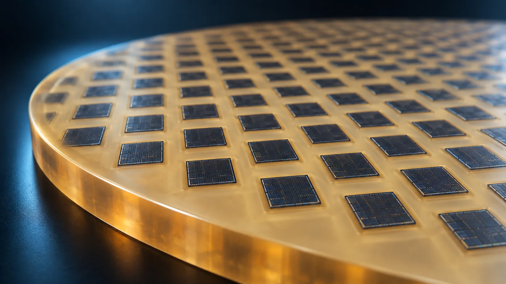
Mounting a die on a substrate used to be a given. Fan-out throws the substrate away. Singulated dies are laid out again on a carrier, moulded into an artificial wafer, and wired directly on top of that. What follows is a swap of roles: the mold compound becomes the structural material, and the redistribution layer takes over the substrate's job.
- What fan-out is (the short version)
- How it differs from fan-in — pushing the terminals outside the die
- Chip-first or chip-last
- A materials engineer's view (1): the mold compound becomes the substrate
- A materials engineer's view (2): how fine the RDL is defines the generation
- Going bigger — from wafer to panel
- What is still hard
- Glossary / Primary sources / Claim-to-source audit
Sourced = a value stated in published material from a research institute or manufacturer (link given)
Our calculation = a figure this article derived, with the assumptions spelled out
Not yet confirmed = research-stage work with no confirmed production record
Anything that is our own structural reading or materials-design interpretation is set apart as Commentary.
1. What fan-out is (the short version)
ASE defines fan-out packaging as "any package with connections fanned-out of the chip surface, enabling more external I/Os"Sourced.
The structural point sits in the next sentence. "Conventional fan-out packages use an epoxy mold compound to fully embed the dies, rather than placing them upon a substrate or interposer."Sourced. In other words, the dies are not put on anything. They are buried in something.
The process is spelled out just as plainlySourced.
- Dice the chips on a silicon wafer
- Position the known-good chips very precisely on a thin reconstituted wafer or panel
- Mould the whole thing in resin
- Form a redistribution layer (RDL) on top of the moulded area — over the dies and over the fan-out region alike
- Form solder balls on top of that
The odd part is step 2: chips that were just cut apart are carefully laid out again into the shape of a wafer.
The reason is equipment. The tools that build an RDL — steppers, plating lines — are built to handle wafers. So if you make the dies pretend to be a wafer, the front-end tool base and its process know-how carry straight over.
And this pretend wafer is mostly resin, not silicon. Every problem in the second half of this article grows out of that one fact (Commentary).
2. How it differs from fan-in — pushing the terminals outside the die
Fan-in came first. In ASE's account the difference is simply which way the traces runSourced.
- Fan-in WLP: "All RDL traces are routed in towards the center of the die"
- Fan-out WLP: "RDL traces are routed both inwards and outwards beyond the limits of the die"
And the ceiling fan-in runs into: "Fan-In WLP faces processing challenges as the area available for I/O layout is limited to the die surface."Sourced. The terminals can only live where the silicon is.
Put in some dimensions and a ball pitch, and count the terminals each approach can holdOur calculation.
- Assumptions: die 5 × 5 mm, package 8 × 8 mm, ball pitch 0.4 mm
- Fan-in: 5 ÷ 0.4 = 12.5 → 12 per edge → 12 × 12 = 144 terminals
- Fan-out: 8 ÷ 0.4 = 20 → 20 per edge → 20 × 20 = 400 terminals
- Ratio = 400 ÷ 144 ≈ 2.8×
Assumptions: every dimension here is one this article invented. Real designs carry keep-out regions and an outer margin, so the count never comes out this clean. The underlying relation holds anyway: 2.56 times the area is 2.56 times the terminals (8² ÷ 5² = 2.56).
That is why ASE lists "Die Shrinkage: Fan-Out allows ball placement beyond the die area" as a featureSourced. Read it the other way round: you can shrink the die and keep the terminal count. The silicon bill goes down (Commentary).
ASE also sorts the benefits by what you are comparing fan-out againstSourced.
| Compared against | Advantages ASE lists (its own wording) |
|---|---|
| Flip chip | Slightly smaller footprint / Lower profile / Better electrical performance / Better thermal performance / Substrate-less package / SiP and 3D integration advantage |
| Fan-in WLCSP | Higher board-level reliability / Fan-out area to counter the pad limitation issue / The use of known good die (KGD) / Better thermal performance / Built-in back-side protection / No restriction in bump pitch / SiP and 3D integration advantage |
From ASE's "Fan-Out Packaging" page [Source 1]. The bold emphasis is ours.
3. Chip-first or chip-last
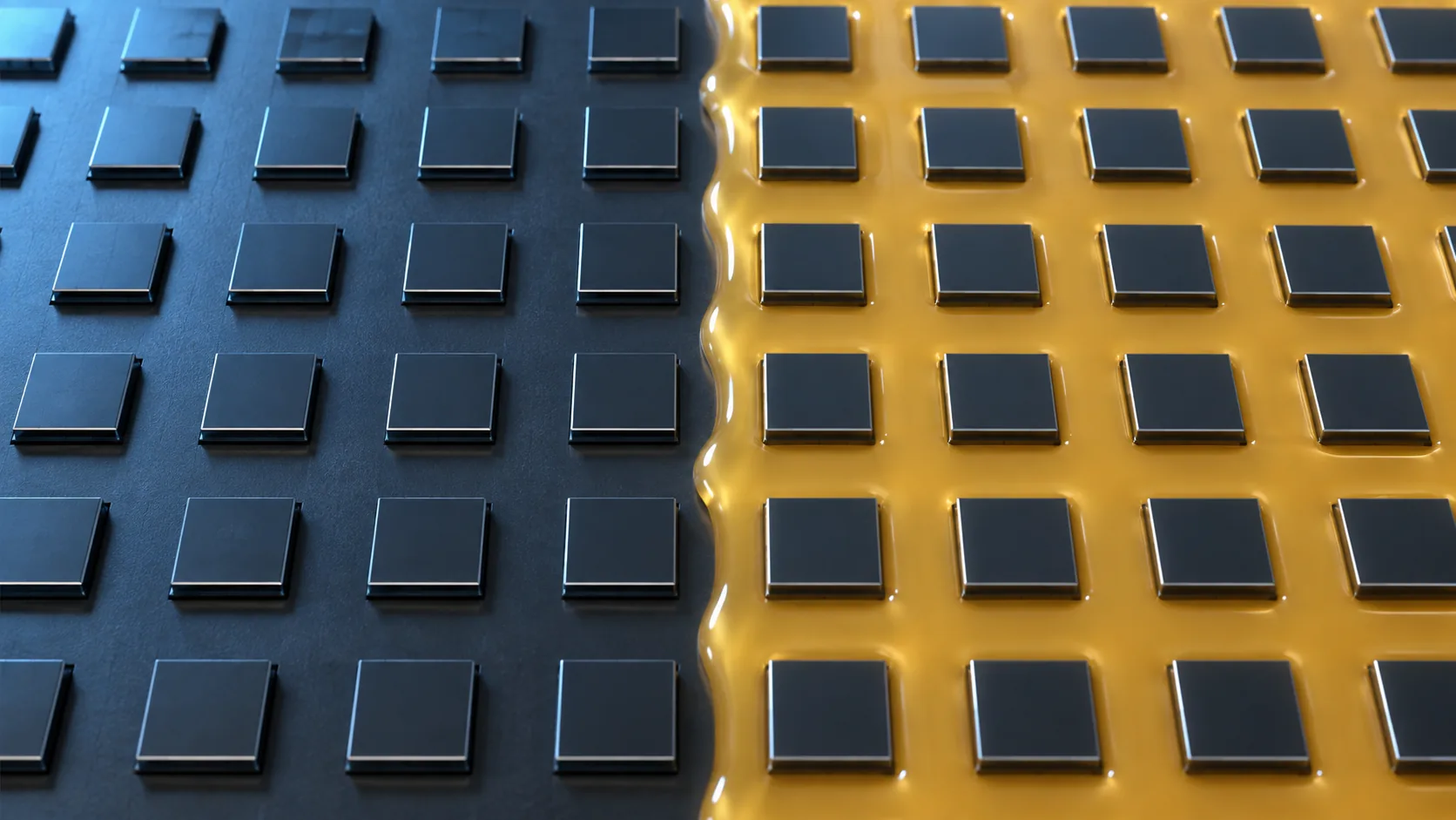
The biggest fork in the fan-out world is whether the dies go down first, or the wiring does. ASE describes three routesSourced.
For chip-first, ASE lists the difficulties as "die shift, die protrusion, wafer warpage and RDL scaling", and says this "limits its usage for complex multi-chip packaging and system-in-package (SiP) with passives integration"Sourced.
Chip-last inverts the order: "molding is conducted after chips are secured on the RDL with flip chip bonds, thereby eliminating die shift, die protrusion and wafer warpage issues during the RDL fabrication"Sourced.
The die shift that chip-first suffers from is, as the PLP article set out in detail, caused by the mold compound shrinking as it cures.
So it is not a placement-accuracy problem. You can put the die down perfectly and the resin will still move it. Which splits the countermeasures in two.
- Solve it in the material: formulate a mold compound that shrinks less (the granular compounds that cut warpage, covered in the Underfill article)
- Solve it in the sequence: cure the resin after the wiring is made, not before (chip-last)
Chip-last reads as a materials problem routed around by process order. The price is a step that handles dies one at a time — the same per-die bonding cost the Bonding article described, showing up again here (Commentary).
4. A materials engineer's view (1): the mold compound becomes the substrate
The defining feature of fan-out fits into one phrase from ASE's list: "Substrate-less package"Sourced. There is no substrate. So who does its work?
Two answers: the epoxy mold compound, and the redistribution layer.
As the Underfill article described, a mold compound was there to protect the die, insulate it, spread its heat and make it handleableSourced.
In fan-out, one more item joins that list: hold the whole thing up as a structure. With no substrate, the resin sets the package outline, supplies the stiffness, and decides the warpage.
Which moves the requirements up a level.
- Cure shrinkage: if it contracts while setting, the dies move (die shift)
- CTE: stray too far from silicon and the package bows every time the temperature changes
- Flatness: 2 µm wiring gets patterned on this surface, so the surface cannot undulate
- Grindability: it may be ground back to expose the die backside
From a material that covers to a material that carries. That shift is the reason the spread of fan-out created a whole new product family for mold compound suppliers (Commentary).
5. A materials engineer's view (2): how fine the RDL is defines the generation
ASE publishes its fan-out products together with the RDL line and space (L/S), the layer count and the year each startedSourced. That one table is, in effect, the history of fan-out.
| Product | Application | Package size (mm) | RDL L/S | RDL layers | From |
|---|---|---|---|---|---|
| eWLB | BB, RF, Codec, Car Radar | up to 12 × 12 | 12/12 µm | 2 | 2009 |
| FOPoP | AP & Memory | up to 15 × 15 | 5/5 µm | 3 | 2016 |
| FOCoS | Networking, Server | up to 67 × 67 | 2/2 µm | 3 | 2016 |
| FOSiP | RF, FEM, Power, MCU | up to 15 × 15 | 5/5 µm | 5 | 2017 |
| M-Series | RF, BB, PMIC, Codec | up to 12 × 12 | 8/8 µm | 2 | 2018 |
| Panel FO | RF, FEM, Power, Server | up to 67 × 67 | 2/2 µm | 5 | 2019 |
From the product list on ASE's "Fan-Out Packaging" page [Source 1]. ASE states that eWLB is licensed from Infineon (Chip-First, Face-Down), M-Series from Deca Technologies (Chip-First, Face-Up), and that FOCoS is its own development.
The line to follow in that table is 12/12 → 8/8 → 5/5 → 2/2 µmSourced. And 2/2 µm appears only on the large packages (up to 67 × 67 mm).
What does going finer demand? The RDL article went through it.
- Photosensitive resin resolution: a 2 µm opening, opened repeatably
- Flatness underneath: an undulating mold surface throws the exposure out of focus
- Plating uniformity: filling narrow trenches evenly (the additive chemistry from the Via article)
Amkor says the same of HDFO: "Interconnect density down to 2/2 µm", with "Polymer dielectrics" as the insulating materialSourced. It makes a point of the fact that HDFO uses organic dielectrics rather than silicon and inorganic films.
Down to 2 µm without going to silicon. That is fan-out's answer to the question the RDL and Interposer articles kept circling: how far can organic materials be pushed before you have to give up on them (Commentary).
Combining it with a bridge
ASE's FOCoS-Bridge goes one step further: "The Si bridge die (L/S 0.6/0.6 um) are embedded in the fan-out RDL layer (L/S 10/10 um) for making the connection between ASIC and HBM."Sourced.
What is happening here is the principle from the Bridge article taken to its conclusion: go fine only where fine is needed.
0.6/0.6 µm on the stretch between ASIC and HBM. 10/10 µm everywhere else. A roughly 17-fold difference in line width, inside one packageOur calculation.
The finest wiring can only be drawn in silicon, so the silicon gets embedded. Whatever organic materials can carry, they carry — the same partitioning by what each material is good at, showing up once more (Commentary).
6. Going bigger — from wafer to panel
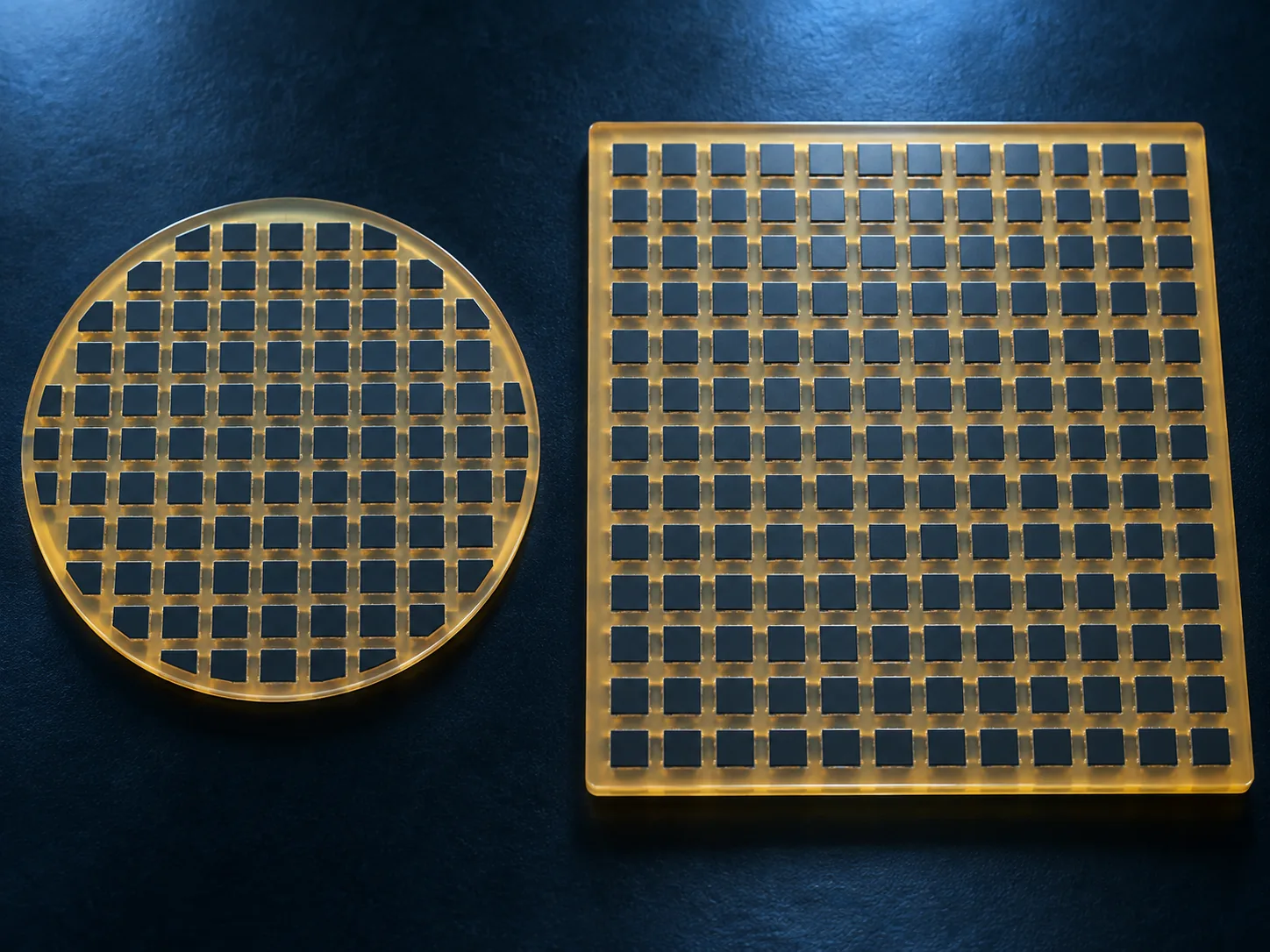
ASE puts panel-level fan-out like this: "By using a rectangular panel as the reconstituted carrier, panel level fan-out (Panel FO) offers the potential for lower production cost due to higher area utilization ratio of the carrier and better economical manufacturing, especially for large packages."Sourced. A circle wastes its corners; a rectangle does not.
The part worth noticing is that panel size is chosen by application: "300 x 300 mm panels for high-density solution (Chip-Last), 600 x 600 mm panels for low-density solution (Chip-First)"Sourced.
ASE's split says the trade-off out loudSourced.
- 300 × 300 mm + chip-last → high density
- 600 × 600 mm + chip-first → low density
Four times the area means more warpage, a tighter placement-accuracy budget, and harder lithography. So the big panel gives up fine wiring, and the small panel gives up units per panel.
The pattern the PLP article described — bigger is cheaper, and bigger is harder — has here hardened into two separate product lines (Commentary).
7. What is still hard
(1) It threw the substrate away, and then went back to it
Fan-out's headline was "Substrate-less package"Sourced. Yet in the large, high-I/O segment the mainstream approach is to mount the fan-out package on a substrate.
ASE defines FOCoS as "a fan-out package flip-chip mounted on a high pin count ball grid array (BGA) substrate"Sourced. Amkor describes S-SWIFT in almost the same words: "Fan-out package flip-chip mounted on a high pin count BGA substrate"Sourced.
Fan-out has widened from "the technology that removes the substrate" to "the technology that adds a fine wiring layer on top of one" (Commentary). And in that role, what it is replacing is the silicon interposer. On FOCoS, ASE writes "FOCoS eliminates the need for an interposer which helps to reduce the package cost."Sourced.
(2) Warpage scales with the area of resin
Amkor lists among S-SWIFT's benefits "lower costs compared to 2.5D, a thinner package, reduced insertion loss, improved impedance control, and lower warpage"Sourced. That "lower warpage" sits in a list of selling points, which is another way of saying warpage is the thing everyone is watching (Commentary).
As the Underfill article set out, warpage comes from CTE mismatch and cure shrinkage. In fan-out the resin is most of the package. The more resin area there is, the more warpage tells — which is exactly why the 600 × 600 mm panel is assigned to low-density work (Commentary).
(3) The assumption that the dies are already good
ASE's process description contains the phrase "very precisely positioning the known-good chips"Sourced. Fan-out starts from dies that are already known to be good.
The company lists "The use of known good die (KGD)" as an advantage over fan-in WLCSP, and "less KGD yield concerns" as an advantage of chip-lastSourced. The KGD problem from the Test article turns up here as a precondition (Commentary).
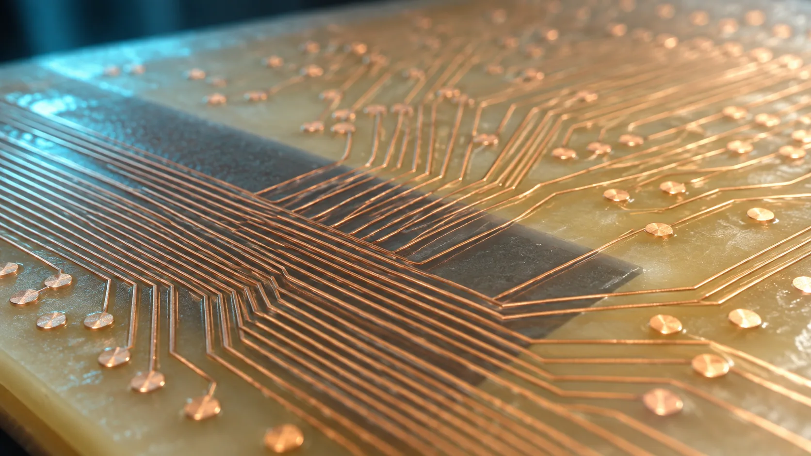
Fan-out is the technology that replaced the substrate with resin plus an RDL. And in doing so it reshuffled what the materials are for.
- Mold compound: a material that covers → a structural material that carries (shrinkage, CTE and flatness become product performance)
- RDL: redistribution on a die → a stand-in for substrate wiring (12/12 to 2/2 µm, and 0.6/0.6 µm once a bridge is added)
- Process order: the fork between chip-first (cheap) and chip-last (fine)
- Carrier: round wafer to square panel — but size and fineness will not come together
The most telling point is that fan-out set out as "no substrate" and is now used as a high-density wiring layer that sits on one. Standing in for the silicon interposer is where this technology currently is (Commentary).
8. Glossary
- Fan-out
- A package style that fans the connections out past the chip surface, allowing more external I/Os.
- Fan-in
- Routing that runs only towards the centre of the die. The terminals stay within the die area.
- WLP
- Wafer Level Packaging. Building the package while the parts are still in wafer form.
- WLCSP
- Wafer Level Chip Scale Package. A wafer-level package roughly the size of the die itself.
- Reconstituted wafer
- An artificial wafer made by laying singulated dies out on a carrier and moulding them in resin.
- Chip-first
- Placing and moulding the dies first, then building the RDL on top.
- Chip-last (RDL first)
- Building the RDL first and bonding the dies to it afterwards.
- Die shift
- Dies moving out of position, mainly through cure shrinkage of the mold compound (covered in the PLP article).
- Die protrusion
- A die standing proud of the moulded surface.
- RDL
- Re-Distribution Layer (covered in the RDL article).
- L/S
- Line / Space. Trace width and the gap between traces. Smaller is finer.
- eWLB
- embedded Wafer Level Ball-grid array. An early fan-out approach.
- FOCoS
- Fan-Out Chip on Substrate. A fan-out package flip-chip mounted on a substrate.
- HDFO
- High Density Fan-Out. Amkor's SWIFT and S-SWIFT are examples.
- Panel level
- Using a square panel rather than a round wafer as the carrier (covered in the PLP article).
- KGD
- Known Good Die. A die that has been tested and shown to be good (covered in the Test article).
- Warpage
- Deformation of the package caused by CTE mismatch and cure shrinkage.
9. Primary sources
- ASE "Fan-Out Packaging" — ase.aseglobal.com
- ASE "FOCoS (Fan-Out Chip on Substrate)" — ase.aseglobal.com
- Amkor "SWIFT® HDFO" — amkor.com
- Amkor "S-SWIFT™ Silicon Wafer Integrated Fan-Out" — amkor.com
10. Claim-to-source audit
| Claim in the text | Basis | Label |
|---|---|---|
| That fan-out is "any package with connections fanned-out of the chip surface, enabling more external I/Os". That "Conventional fan-out packages use an epoxy mold compound to fully embed the dies, rather than placing them upon a substrate or interposer." That the process is "dicing chips on a silicon wafer, and then very precisely positioning the known-good chips on a thin "reconstituted" or carrier wafer/panel, which is then molded and followed by a redistribution layer (RDL) atop the molded area...and then forming solder balls on top". That fan-in is "All RDL traces are routed in towards the center of the die" and fan-out is "RDL traces are routed both inwards and outwards beyond the limits of the die". That "Fan-In WLP faces processing challenges as the area available for I/O layout is limited to the die surface." That "Die Shrinkage: Fan-Out allows ball placement beyond the die area". The advantages over flip chip (six items including Substrate-less package) and over fan-in WLCSP (seven items including KGD and No restriction in bump pitch). That chip-first "provides a lower cost solution suitable for low I/O applications" with difficulties "die shift, die protrusion, wafer warpage and RDL scaling". That chip-last "has less KGD (known good dice) yield concerns compared with the Chip-First process", that "molding is conducted after chips are secured on the RDL with flip chip bonds, thereby eliminating die shift, die protrusion and wafer warpage issues during the RDL fabrication", and that it "allows ultra-fine pitch scales e.g. 2um". That Panel FO "offers the potential for lower production cost due to higher area utilization ratio of the carrier" and uses "300 x 300 mm panels for high-density solution (Chip-Last), 600 x 600 mm panels for low-density solution (Chip-First)". The product list (eWLB 12/12 µm, 2 layers, 2009 / FOPoP 5/5 µm, 3 layers, 2016 / FOCoS 2/2 µm, 3 layers, 2016 / FOSiP 5/5 µm, 5 layers, 2017 / M-Series 8/8 µm, 2 layers, 2018 / Panel FO 2/2 µm, 5 layers, 2019, with their package sizes and applications). That eWLB is licensed from Infineon and M-Series from Deca Technologies | ASE "Fan-Out Packaging"[Source 1] https://ase.aseglobal.com/en/technology/fan_out | Sourced |
| That FOCoS is "a fan-out package flip-chip mounted on a high pin count ball grid array (BGA) substrate". That "FOCoS eliminates the need for an interposer which helps to reduce the package cost." That in FOCoS-Bridge "The Si bridge die (L/S 0.6/0.6 um) are embedded in the fan-out RDL layer (L/S 10/10 um) for making the connection between ASIC and HBM." That FOCoS-CF has "no micro-bumps between the Si dies and fanout RDL (L/S 2/2 um)". That it targets high I/O counts (>1000) | ASE "FOCoS"[Source 2] https://ase.aseglobal.com/focos/ | Sourced |
| That SWIFT / HDFO offers "Interconnect density down to 2/2 µm". That the dielectric is "Polymer dielectrics". That it supports "Multi-die and large die capability" and "Large body package capability" | Amkor "SWIFT® HDFO"[Source 3] https://amkor.com/technology/swift/ | Sourced |
| That S-SWIFT is a "Fan-out package flip-chip mounted on a high pin count BGA substrate". That it "Eliminates the need for an interposer, reducing package costs", "Offers lower costs compared to 2.5D, a thinner package, reduced insertion loss, improved impedance control, and lower warpage", and "Supports high I/O counts (>1000)" | Amkor "S-SWIFT™"[Source 4] https://amkor.com/technology/s-swift/ | Sourced |
| The terminal counts obtained by assuming a 5 × 5 mm die, an 8 × 8 mm package and a 0.4 mm ball pitch (144 and 400, about 2.8 times), and the area ratio 8² ÷ 5² = 2.56 | Our calculation. Every dimension is an assumption made by this article, and no allowance is made for the outer margin or keep-out regions | Our calculation |
| The line-width ratio in FOCoS-Bridge, 10 ÷ 0.6 ≈ about 17 times | Our calculation. The underlying values come from Source 2[Source 2] https://ase.aseglobal.com/focos/ | Our calculation |
| That Fig. 5 lines up products with different applications and package sizes on the single axis of L/S and is not a ranking. That the relative size of the squares in Fig. 7 does not match real dimensions | Our note. The numbers themselves come from Sources 1 and 2 | Commentary |
| The explanation that the reconstituted wafer exists so that RDL equipment can be reused. The account of the mold compound changing from a material that covers to a structural material that carries (shrinkage, CTE, flatness, grindability). The reading that die shift is a resin-shrinkage problem rather than a placement-accuracy one, and that chip-last routes around a materials problem through process order. The list of what going below 2 µm requires (resist resolution, flatness underneath, plating uniformity). The observation that the role has widened from "no substrate" to "a high-density wiring layer on top of a substrate". The reading that warpage scales with resin area, which is why 600 × 600 mm is assigned to low-density work | Our own organisation and commentary based on published material. Not a position stated by any of the companies | Commentary |
| That Figs. 1, 3, 4, 5 and 7 are drawings made to explain, not observed images or design data | Our note | Commentary |
Last updated 20 September 2026. Sources are limited to primary material (official technology pages published by the package manufacturers). Because this article also contains our own structural organisation and materials-design reading, those parts are set apart as Commentary and kept distinct from sourced fact. All figures are explanatory concept graphics. Visual-overview figures are shown as AI-generated conceptual images, matching the Japanese edition. Vector drawings are retained where they carry quantitative values or precision-critical technical labels. AI-generated images do not depict real equipment, products, facilities, dimensions or exact cross-sections; replaced source SVG overview drawings remain in the HTML but are hidden.