MENU

Bonding Explained

Back to Technology & Company Guides

TECHNOLOGY EXPLAINER

What Bonding Is
— heat, pressure and ultrasound, for sticking metal to metal

A semiconductor package is a set of separate parts wired electrically together. Making those joins is bonding. From wire bonding, in service for more than sixty years, to the newest joining aimed at 5 µm pitch, this step is made, throughout, of choices about materials.
Built from published material by Nippon Micrometal, NSC (Nippon Steel Chemical & Material), ASMPT, Kulicke & Soffa, Amkor, Resonac, Mitsubishi Materials and Kyocera / Last updated September 2026

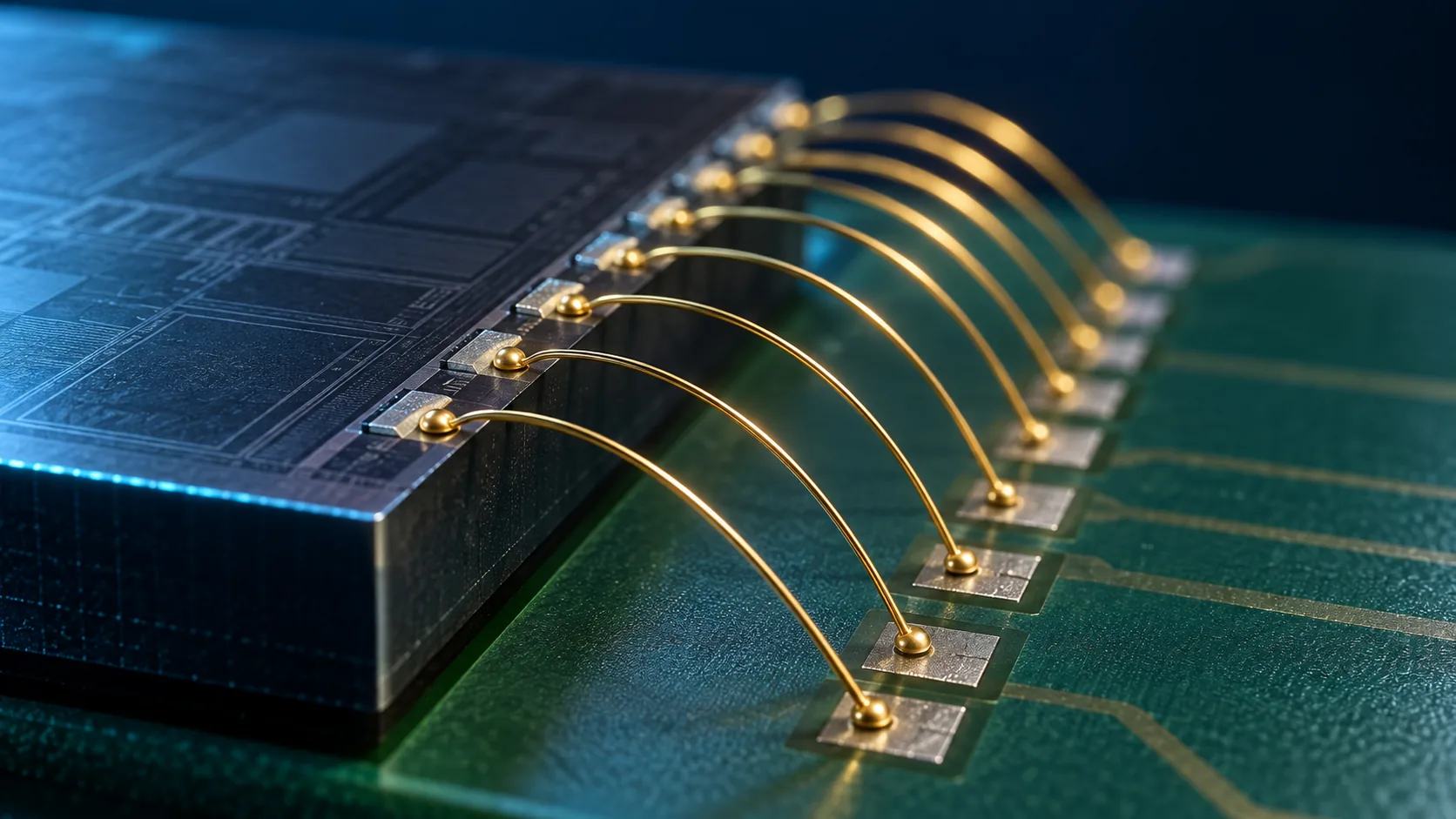
Magnified conceptual image of a fine metal wire arching from the electrode of a semiconductor chip across to the substrate
Conceptual image (AI-generated). An impression of bonding. It does not represent real wire diameter, count, loop shape or dimensions.
What this article covers
  1. What bonding is (the short version)
  2. Why sticking things together is hard
  3. A map of joining — what is joined where in a package, and with what
  4. Wire bonding — a technology still in use after sixty years
  5. A materials engineer's view 1: from gold to copper, and on to silver
  6. Flip chip and TCB — turn it over and join across the face
  7. A materials engineer's view 2: die bonding is a contest between a film and a powder
  8. What is still hard
  9. Glossary / Primary sources / Claim-to-source audit
How claims are labelled in this article

Sourced = content stated in a company's published material (link given)
Our calculation = a figure this article derived, with the assumptions spelled out
Not yet confirmed = a plan with no confirmed track record
Beyond those, process framing and readings about materials design are marked Commentary.

1. What bonding is (the short version)

Bonding is the step that joins separately made parts together in a state where current can flow. Boiled down, the semiconductor back end is that operation repeated.

  • What gets joined: chip to substrate, chip to chip, chip to lead frame, package to motherboard
  • What joins them: a fine metal wire, a bead of solder (a bump), an adhesive film, a metal paste, or direct bonding of the metals themselves
  • What does the joining: heat, pressure (load) and ultrasound. Whatever the method, those are broadly the three tools

Nippon Micrometal describes bonding wire as "a fine metal wire that carries the electrical signals of a semiconductor element to the outside", and the joining step as "bonding the ball to the semiconductor element using heat, ultrasound and load (the first bond)"Sourced. That set of three, heat, ultrasound and load, is the spine of this article.

The first thing that trips people up

Hearing "stick together", you may picture glue or welding. But most semiconductor joining involves no melting at all. Metals are pressed against one another, the dirt and oxide on the surface is broken up, and they are brought close enough for atoms to diffuse across. Joining without melting — that is the first thing to get past.

2. Why sticking things together is hard

Press two clean metals together and in principle they join. In practice they do not. There are three reasons.

(1) The surface is oxidised

Aluminium and copper both grow an oxide the instant they meet air, and oxide is an insulator. Press them together and that film stays trapped in between. (The Test article described a probe needle breaking an oxide; the same problem turns up here.)

(2) The surface is not flat

Under a microscope, any metal surface is rough. Press two together and what actually touches is only the peaks. The contacting area is far smaller than the apparent area.

(3) Semiconductors do not like heat

So melt it at high temperature, then? No. Fine wiring is built into the top of the chip, and organic substrates warp as temperature rises. The temperature needed to make the join and the temperature the parts can survive are always in tension.

Which is why all three of heat, load and ultrasound are used

The move that solves all three troubles at once is ultrasound.

  • Load flattens the roughness and increases the area actually in contact
  • Ultrasound scrubs laterally in tiny strokes, cracking the oxide and exposing fresh metal
  • Heat makes the atoms mobile, driving diffusion and stabilising the joint

With ultrasound you can join without melting, and at a comparatively low temperature. That is one reason wire bonding has stayed in active service for more than sixty years (Commentary).

3. A map of joining — what is joined where in a package, and with what

The single word "bonding" covers a lot of ground, so let us first sort it by location.
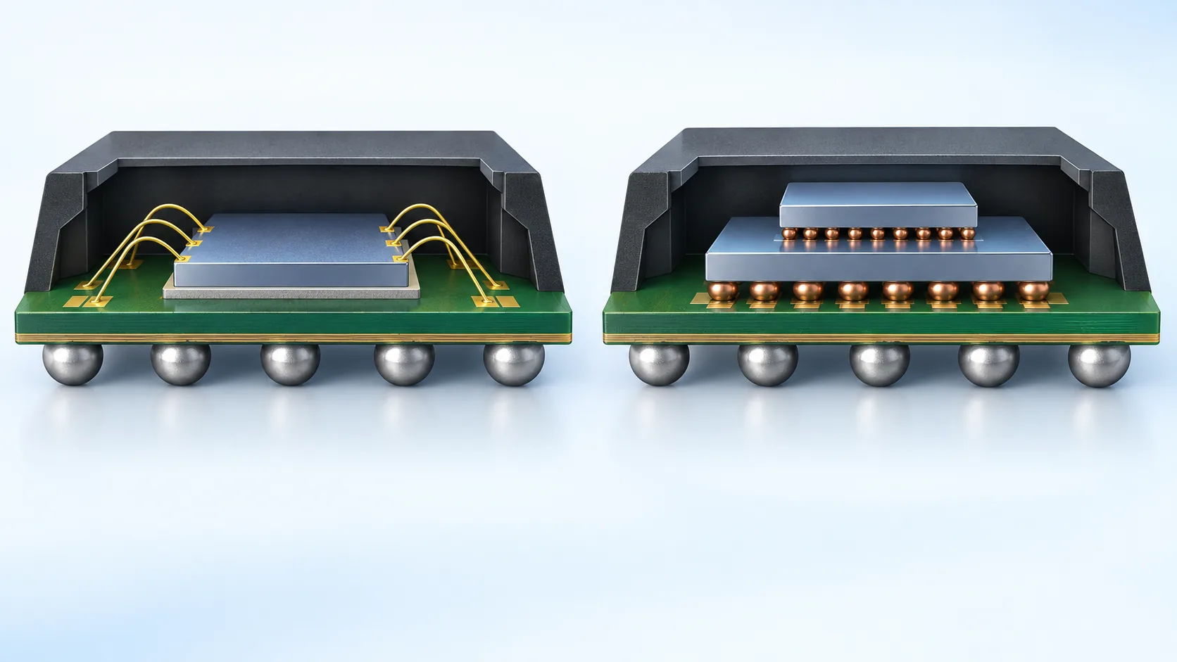
Fig. 1 · Map of the joining locations inside a package
Conceptual illustration of Map of the joining locations inside a package
Fig. 1 Conceptual image (AI-generated). The structure is schematic and does not show real dimensional ratios, bump counts or wire counts. This article deals mainly with 1, 2 and 3.

This article works through 1. die bonding, 2. wire bonding and 3. flip chip and die-to-die joining in turn. The leading edge of 3, hybrid bonding (joining Cu directly to Cu without solder), is covered in detail in the separate Hybrid Bonding article.

4. Wire bonding — a technology still in use after sixty years

According to Nippon Micrometal, "the wire bonding method of connection was developed in the late 1950s by researchers at Bell Laboratories in the United States"Sourced. It is a technology almost exactly as old as the semiconductor itself.

The wire used runs "from as fine as 15 µm to as thick as around 500 µm". In high-performance packages the wires are "strung at intervals of roughly 30 to 50 µm"Sourced. A human hair is about 80 µm across, so the fine end is about a fifth of a hair.
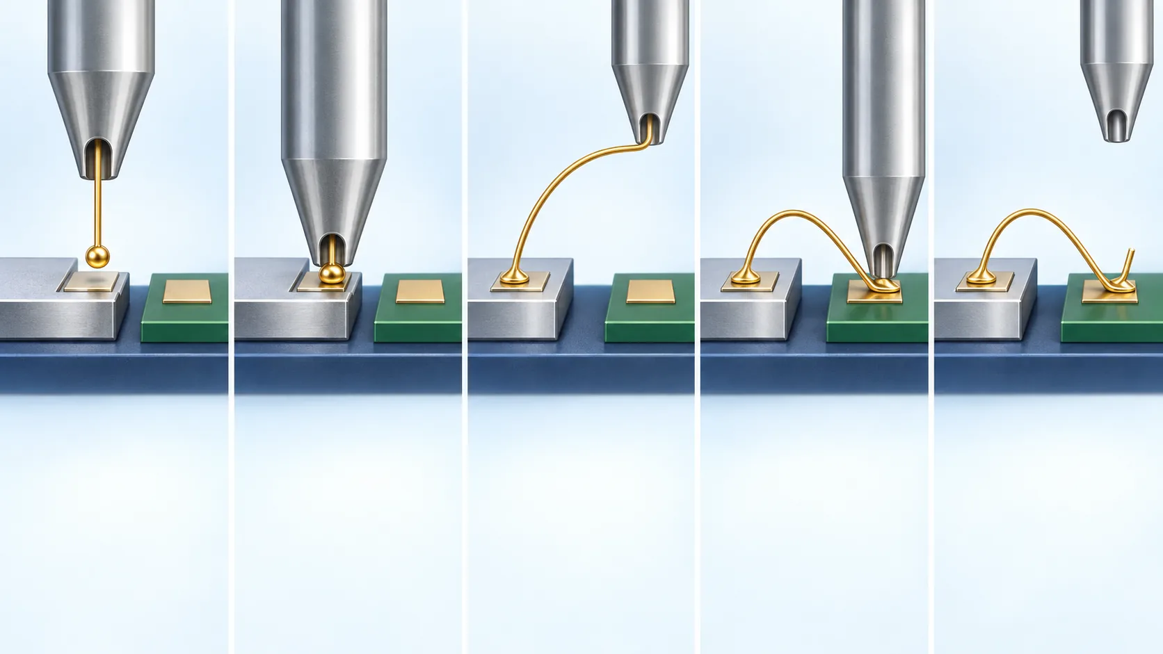
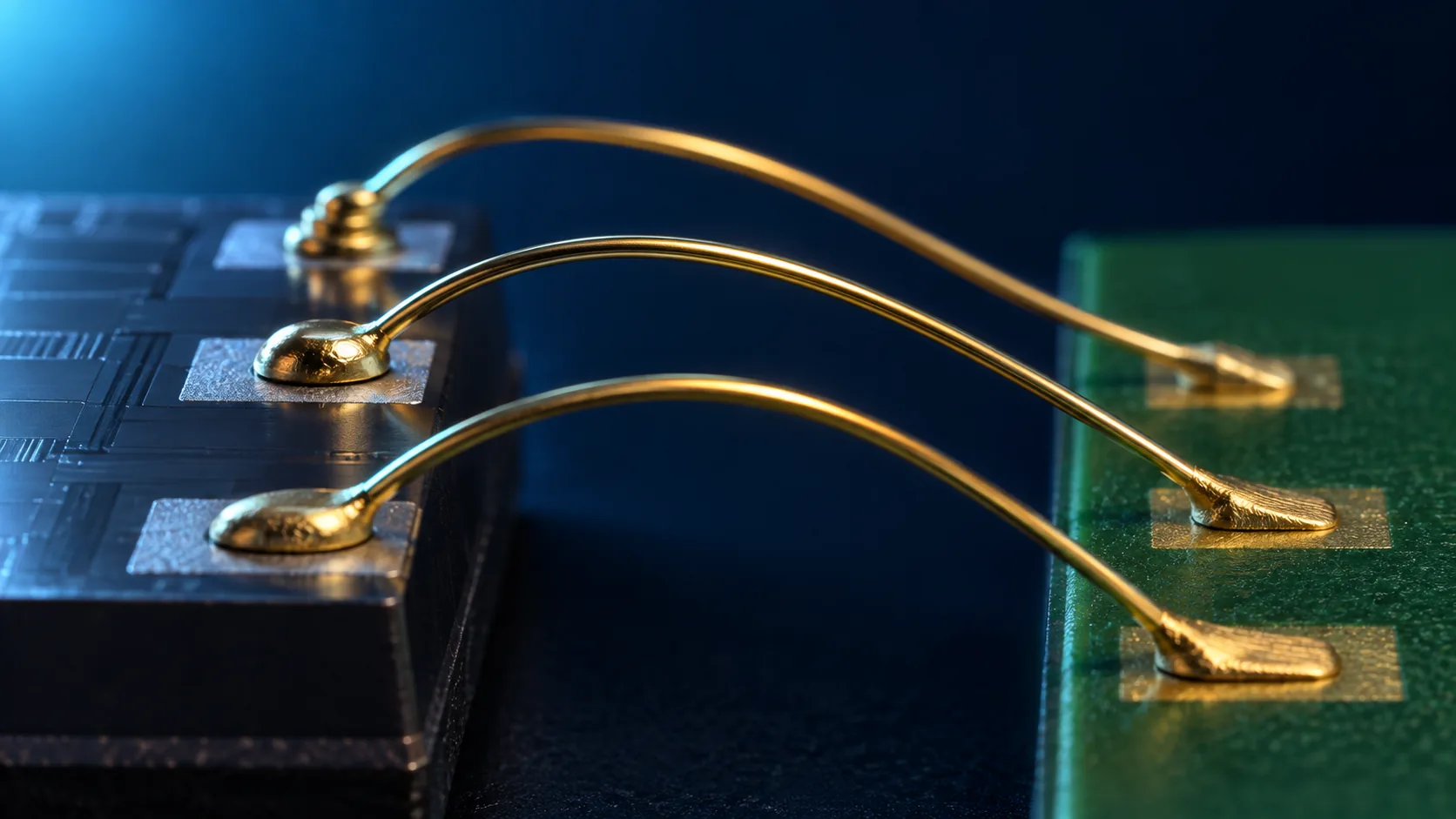
Fig. 2 · One cycle of wire bonding
Conceptual illustration of One cycle of wire bonding
Fig. 2 Conceptual image (AI-generated). The size ratios of capillary, wire and chip are schematic and do not show real shapes. The step names — ball forming by electrical discharge, the first bond by heat, ultrasound and load, and the stitch bond — follow Nippon Micrometal's description [Source 1]. The figure of tens of milliseconds per wire is a general order of magnitude noted by this article, not a published value for any particular machine.
Magnified conceptual image of many fine gold wires arching from electrodes along the edge of a semiconductor chip down to the substrate
Fig. 3 Conceptual image (AI-generated). An impression of wires in place. It does not accurately depict real wire diameter, count, spacing or loop shape.

The conditions under which things stick have width

Here an important term appears that you only find in materials suppliers' literature: the process window.

Nippon Micrometal lists "a very wide process window" among the features of its aluminium wire NL1, publishing the evaluation conditions as 300 µm wire diameter, 700 cN bonding force, shear strength > 1250 cN, and squash width < 1.3 times the wire diameterSourced.

What does that mean? It means there is a range in which two conditions are met at the same time: the joint is strong enough, and yet it has not been squashed too far.

Join with three tools, and look for the sweet range (conceptual) The three tools of joining Load Flattens roughness Ultrasound Cracks the oxide Heat Drives diffusion Joint No one of them works alone. Too much or too little of any one of them and the joint is not stable. Bonding conditions have a window Vertical: shear strength. Horizontal: squash width 1250cN 1.3 x wire dia. OK Weak bond Over-squashed Red dashes = NL1 criteria: 1250 cN or more, 1.3 x dia. or less. Too far left it will not stick; too far right it damages the chip.
Fig. 4 Conceptual diagram (vector drawing). The shape of the curves is schematic, not measured data. The thresholds, shear strength > 1250 cN and squash width < 1.3 times the wire diameter, are the values Nippon Micrometal publishes as its evaluation conditions for the aluminium wire NL1 (300 µm wire diameter, 700 cN bonding force) [Source 5].
Why this matters for materials engineers: the width of the window is the product's value

When a materials supplier advertises "a wide process window", that is not a claim about absolute performance. It means "it still bonds properly when conditions drift a little".

On a production floor the machine warms up, the capillary wears, the lot changes. Conditions always spread. So you need a window they will not drift out of. This is exactly the same picture as the needle penetration depth in the Test article. Not a single perfect point but how wide you can make the acceptable range is where materials compete (Commentary).

5. A materials engineer's view 1: from gold to copper, and on to silver

Sixty years of wire bonding is also, straightforwardly, a history of replacing the wire material.

From gold to palladium-coated copper: how wire materials changed All years and events come from Nippon Micrometal's published material Late 1950s at Bell Laboratories Wire bonding developed 2000s Gold price surges (gold dominant for 50 years) 2004 Copper wire development begins 2007 World's first palladium-coated copper wire, EX, developed 2009 EX1 goes on sale Today PCC wire is the most widely used
Fig. 5 Conceptual diagram (vector drawing). Years and events follow Nippon Micrometal's "History of palladium-coated copper bonding wire" and "What is bonding wire?" [Sources 1 and 2]. The spacing along the time axis is not uniform; it has been adjusted for readability.

(1) Why gold was abandoned

Nippon Micrometal states that "gold, used for bonding wire for fifty years, was high in performance but extremely expensive", citing "the surge in the gold price during the 2000s" as the backgroundSourced.

(2) Why copper was hard

Copper is cheap and conducts well. The reason it could not be used for so long is that it oxidises. The company explains that by "coating palladium at the nanometre level on the outside of a wire only about a fifth the thickness of a human hair (15 to 30 µm), we achieved bondability and corrosion resistance that were impossible with conventional copper wire"Sourced.

The current standard product, EX1p, is a gold and palladium coated copper bonding wire with gold over the top of that, described as having "improved second bond (stitch bond) performance compared with EX1" and "a better Pd distribution in the FAB (free air ball)"Sourced.

Three layers on a wire 16 micrometres across

The product photograph of EX1p is marked 16 µm diameterSourced. On the surface of a wire that thin, a palladium layer is formed, and over that a gold layer. And the published spool length runs "up to 5000 m", with the coating uniform over that entire lengthSourced. Surface treatment of 5 km of 16 µm wire, held constant to the nanometre — that is what the phrase "bonding wire manufacturing technology" actually refers to (Commentary).

(3) The other option — silver alloy

Alongside the shift to copper, a path through silver alloy wire has also opened. Nippon Micrometal publishes the following comparison of its GX2s against gold wireSourced.

PropertyGX2s (silver alloy)Au wire (gold)
Purity98%99.99%
Electrical resistivity (RT)2.4 µΩcm2.4 µΩcm
Looping performanceEqual or better—
FAB hardness41 Hv43 Hv

From Nippon Micrometal's GX product page (figures are typical values) [Source 4].

Why this matters for materials engineers: what it means that hardness is in the catalogue

A wire catalogue lists FAB hardness — the hardness of the free air ball made by the electrical discharge. That looks odd, and is in fact the heart of it.

The ball is pressed into the chip electrode. The harder the ball, the more damage the pad and the layers beneath it take. In the Test article, a probe needle that was too hard punched through the pad and wrecked the circuit underneath. Exactly the same thing happens in wire bonding.

Hence the company's line about GX2, that it "has bondability on a par with gold wire and can handle fragile chips"Sourced. And in the numbers, FAB hardness is 41 Hv against gold's 43 Hv, slightly softer, while resistivity is 2.4 µΩcm, the same as goldSourced.

So the pitch for silver alloy wire is not "better than gold". It is the logic of a substitute: "as soft as gold, conducts like gold, and cheaper". When you replace a material, what you have to win on is not performance but equivalence — a basic fact of materials development, showing up unmodified in a product catalogue (Commentary).

(4) Which material goes where

Four kinds of bonding wire coexist All values published by Nippon Micrometal and NSC (Nippon Steel Chemical & Material) Gold (Au) AT series (4N grade) Purity 99.99% or more FAB hardness 43 Hv Resistivity 2.4 µΩcm Best for fine wire and low loops. But costly Silver alloy (Ag) GX2 series Purity 98% FAB hardness 41 Hv Resistivity 2.4 µΩcm Works even on fragile chips Pd-coated copper EX series (PCC) Purity 2N or 4N Floor life 30 days Spool up to 5000 m The de facto market standard Aluminium (Al) NL1 series Dia. over 100 to 500 µm NL1F is 100 µm or less High corrosion resist. For power devices and automotive battery joins Note: gold and Pd-coated copper both list long span and fine pitch capability among their features.
Fig. 6 Conceptual diagram (vector drawing). All figures are the companies' published values [Sources 1, 3, 4, 5 and 6]. The four did not replace one another; they coexist, chosen by application. Because price, hardness, corrosion resistance and wire diameter are demanded differently in each application, no single one takes the lot.

Do you need thin wire or thick wire? Is the chip fragile or robust? Will it live somewhere hot and humid? Different demands, different metal. Wire bonding, a sixty-year-old technology, is still alive not because of the equipment but because the materials side has kept following the demands (Commentary).

6. Flip chip and TCB — turn it over and join across the face

Wire bonding has one constraint it simply cannot get past: wires can only come out around the edge of the chip.

Once a chip grows large and needs thousands or tens of thousands of terminals, the edge is not enough. So the chip is flipped over and connected directly to the substrate by bumps laid across its whole face. That is flip chip joining.

(1) Bake them all at once, or press one at a time

There are broadly two ways to make flip chip joints. In describing its own packages, Amkor notes that fine-pitch flip chip connections are made by either "thermocompression with non-conductive paste (TCNCP) or mass reflow with capillary underfill (CUF)"Sourced.
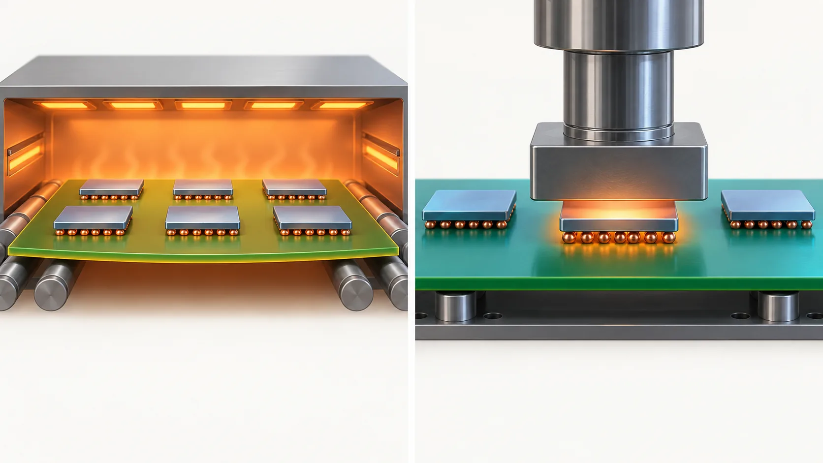
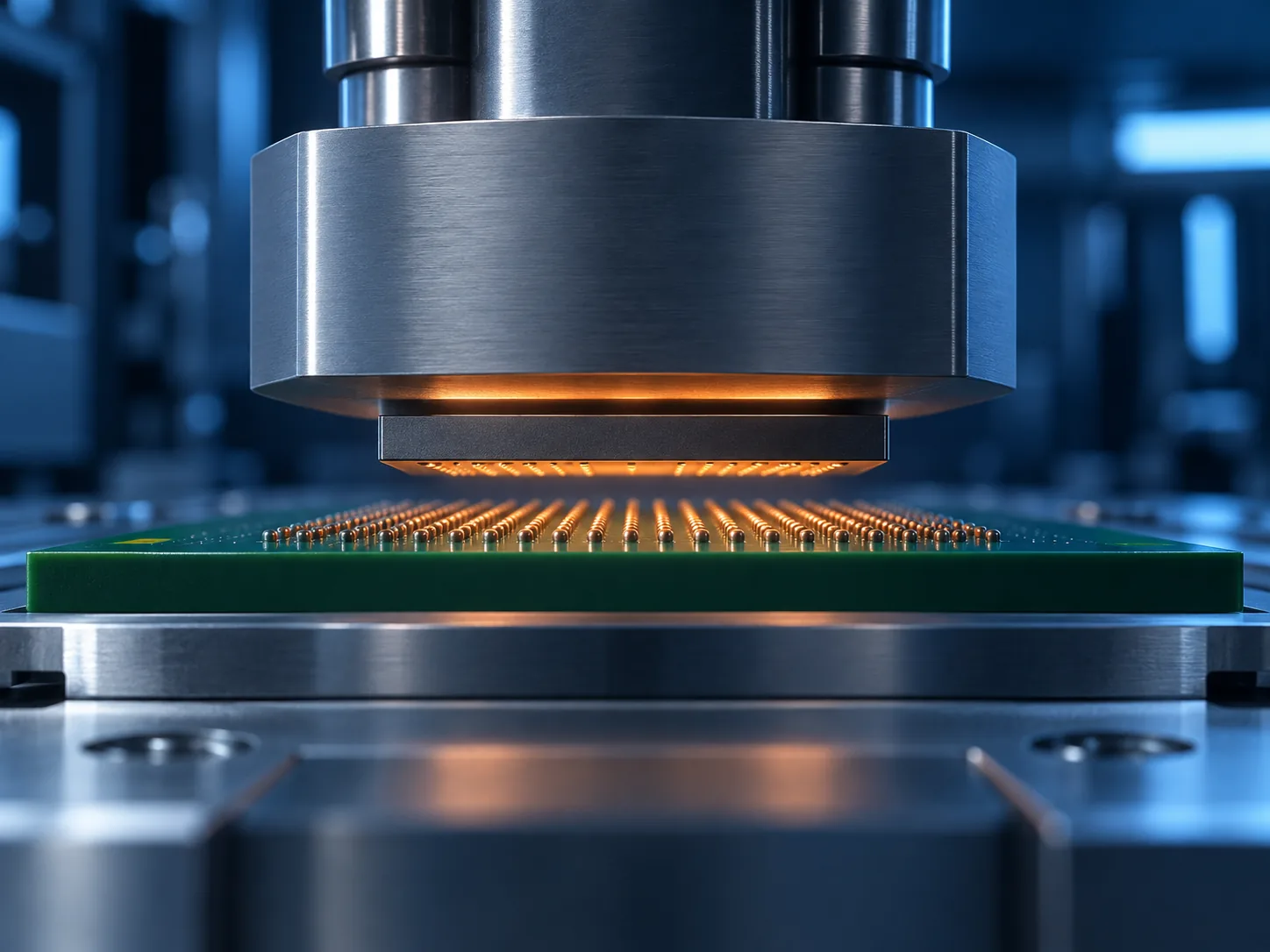
Fig. 7 · Comparison of mass reflow and thermocompression bonding
Conceptual illustration of Comparison of mass reflow and thermocompression bonding
Fig. 7 Conceptual image (AI-generated). Structure and the amount of warpage are schematically exaggerated and do not show real deformation or equipment layout. That the two methods coexist follows Amkor's description (TCNCP and mass reflow with CUF) [Source 7].
Conceptual image of a machine bond head holding a thin semiconductor chip by vacuum and lowering it precisely onto a substrate
Fig. 8 Conceptual image (AI-generated). An impression of a thermocompression bonder working. It does not depict any particular maker's equipment or the real mechanism.

(2) The numbers on TCB

Kulicke & Soffa defines TCB as "a flip-chip bonding process that uses a combination of heat and pressure to create interconnects between chips and substrates"Sourced. On pitch, it gives "down to 10 µm pitch" for solder-based joining and "down to at least 5 µm pitch" for direct copper-to-copperSourced. The company also says it has developed fluxless bonding technologySourced.

On the equipment side, ASMPT publishes for its TCB system FIREBIRD placement accuracy of ±2.0 µm, a cycle time under 2 seconds, and angular accuracy of ±0.01° on large dies and ±0.05° on small onesSourced. It also states "over 250 sets installed in mass production worldwide"Sourced.

Change the joining method and the spacing you can reach changes The horizontal scale is logarithmic (wider spacing to the right) Wire bonding 30 to 50 µm TCB (solder joining) Down to 10 µm pitch TCB (direct Cu-to-Cu) Down to at least 5 µm pitch Hybrid bonding Covered in the Hybrid Bonding article Note: the wire figure is from the statement that in high-performance packages wires are strung at 30 to 50 µm intervals (wire to wire). Note: TCB figures are capable pitches from Kulicke & Soffa. Different things are measured, so it is not a strict comparison.
Fig. 9 Conceptual diagram (vector drawing). Bar lengths are a logarithmic indication and do not represent exact proportions. Wire spacing follows Nippon Micrometal, TCB pitch capability follows Kulicke & Soffa [Sources 1 and 9]. Spacing between wires and bump joining pitch are measurements of different things.
Why "no flux" matters

Soldering normally uses flux, a chemistry that strips the surface oxide. But as pitch gets finer, the flux residue can no longer be washed out. The gaps are too narrow for the cleaning fluid to get in.

When Kulicke & Soffa cites fluxless bonding technology and describes it as "first for solder-based interconnects and most recently for direct copper-to-copper interconnects", it is because direct Cu-to-Cu joining, that is, hybrid bonding lies at the end of that lineSourced. Scaling also works in the direction of leaving you fewer chemicals you are allowed to use (Commentary).

7. A materials engineer's view 2: die bonding is a contest between a film and a powder

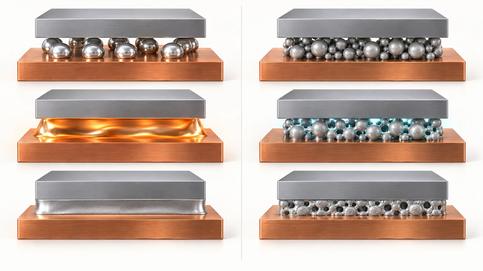
Finally, back to 1. die bonding in Fig. 1. The step that fixes the chip to a substrate or lead frame currently has two material systems running in parallel: a film and a metal paste (a powder).

(1) The film — die attach film (DAF)

On its die attach film integrated with dicing tape, Resonac describes "DAF technology combining low modulus for excellent thermal stress relief with high adhesive strength and excellent heat resistance", and says it has "more than twenty years in the market, with world-leading share in both production volume and sales"Sourced. Applications run "from 3D NAND and DRAM memory devices through to lead frame use"Sourced.

Low modulus, high adhesion and heat resistance do not normally go together

Anyone who has designed a resin should snag on seeing those three phrases in one sentence.

  • Low modulus (soft) absorbs the expansion mismatch between chip and substrate. But adhesion and heat resistance normally fall with it
  • High adhesion and high heat resistance come with higher crosslink density, which makes it hard. Hard means the stress goes straight into the chip

So a DAF is a material made to house contradictory demands in a single film: soft enough to relieve stress, yet it must not peel, and it must survive the heat of the rest of the back end. The picture is identical to the Df, CTE, Tg and modulus trade-off from the Build-up Film article (Commentary).

(2) The powder — silver sintering

In power semiconductors, meanwhile, solder has stopped being enough. Because SiC and GaN devices run hot, the joint fails before the device does.

On its silver sintering paste for die attach, Kyocera cites "strong bonding through metal sintering of nano silver powder and micron silver powder", says "pressureless bonding" is possible with "low-temperature sintering at 200 to 250 °C", and that it "delivers high joint reliability even at 250 °C"Sourced.

On 8 January 2020, Mitsubishi Materials announced a sintering-type joining material for next-generation power modules that "can be bonded pressurelessly to the copper members on the substrate surface without plating precious metal", with joint strength "of 30 MPa or more", heat resistance "of 200 °C or more", and "a joint layer with far fewer voids than conventional products"Sourced.

Fig. 10 · The difference between solder joining and silver sinter joining
Conceptual illustration of The difference between solder joining and silver sinter joining
Fig. 10 Conceptual image (AI-generated). It schematises the flow of the process and does not accurately represent a temperature profile. Sintering temperature, heat resistance and joint strength are published values from Kyocera and Mitsubishi Materials [Sources 11 and 12]. No specific melting point or service temperature is given for the solder side, because the company material this article drew on does not state one.
Why this matters for materials engineers: sintering removes the melting-point constraint

Solder joining is a process of melting above the melting point and freezing on cooling. The inescapable consequence is that raise it back to the joining temperature and it comes apart again. So the service temperature ceiling has to sit below the joining temperature.

Sintering breaks that. Kyocera can write that it joins at "low-temperature sintering, 200 to 250 °C" and still "delivers high joint reliability even at 250 °C" because the particles are being bonded to one another far below the melting point of silverSourced. What comes out is sintered silver, not a low-melting alloy.

What Mitsubishi Materials stresses on top of that is two things: "without plating precious metal" and "pressurelessly"Sourced. No pressure means simpler equipment; no plating means one fewer process step and lower cost. A good example of a material's value being measured not only by joint performance but by how many surrounding process steps it deletes (Commentary).

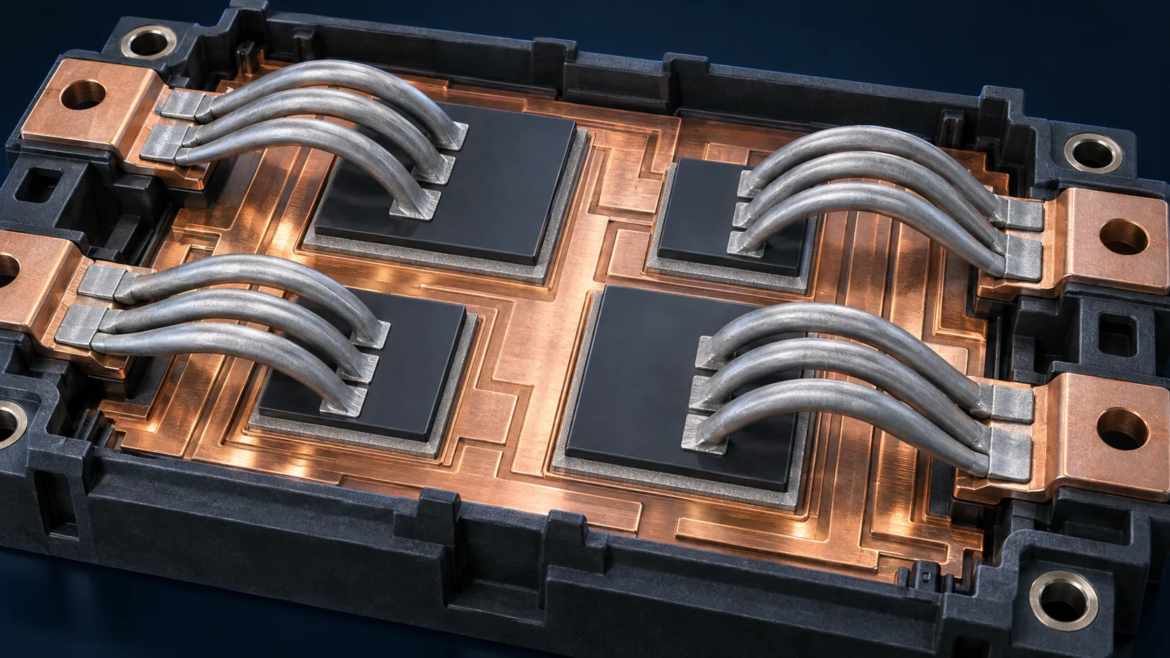
Conceptual image of the inside of a power module, with a large semiconductor chip bonded to a metal substrate and several thick aluminium wires arching across it
Fig. 11 Conceptual image (AI-generated). An impression of the inside of a power module. It does not show the internal structure of any particular product, nor real wire counts or dimensions.

8. What is still hard

(1) The cost of pressing them one at a time

TCB's biggest weakness is that it cannot be batched the way mass reflow can. ASMPT publishes FIREBIRD's cycle time as under 2 secondsSourced.

Our calculation: what happens when two seconds add up

Take a 2-second cycle time and assume the machine never stopsOur calculation.

  • Per machine, 3,600 s divided by 2 s = 1,800 bonds per hour
  • Building an 8-high stack takes 8 bonds per stack
  • So 1,800 divided by 8 = 225 stacks per hour per machine

Assumptions: a theoretical ceiling with no changeover, transport, alignment wait or maintenance downtime at all. Real throughput comes out lower. And the very framing of one bond per layer depends on the process (stacking layer by layer, or joining a stack in one go).

Something still shows through. The deeper the stack, the more bonds, in direct proportion to layer count. Because the "measure many at once" move from the Test article is unavailable here, TCB can only raise throughput by adding machines. ASMPT's emphasis on "over 250 sets installed in mass production worldwide" can be read as the flip side of that propertySourced (Commentary).

(2) Wire bonding is not going away

Talk about advanced packages gathers around flip chip and TCB, but there is no sign of wire bonding disappearing. That Nippon Micrometal keeps five lines in production in parallel — gold, silver alloy, palladium-coated copper, bare copper and aluminium — is itself evidence that the best joint differs by applicationSourced. In power semiconductors especially, thick aluminium wire of over 100 µm up to 500 µm is usedSourced. Carrying large currents takes thick metal.

(3) Material prices move technology choices

The most blunt fact in this article is that a technology was replaced on price. Nippon Micrometal states plainly that behind copper wire development lay "the surge in the gold price during the 2000s" and that "gold, used for bonding wire for fifty years, was high in performance but extremely expensive"Sourced.

It was not displaced because it lost on performance. It was displaced on price. And to displace it, a new materials technology, palladium coating, had to be created — work started in 2004, the world's first development in 2007, sales from 2009. That timeline is itself a demonstration that material substitution takes yearsSourced.

(4) The list of usable chemicals keeps shrinking

The finer the pitch, the less possible it is to wash flux residue out. Kulicke & Soffa putting fluxless bonding forward and positioning what lies beyond it as "direct copper-to-copper interconnects" is because that constraint is one of the forces pushing towards direct Cu-to-Cu joining, that is, hybrid bondingSourced.

How to hold this article in mind

Bonding looks like a story about equipment and is a story about materials.

  • What joins it = gold, silver, copper, aluminium, solder, resin, silver particles
  • How it is joined = the mix of heat, load and ultrasound
  • How close you can pack it = the smallest dimension the material allows
  • When it fails = decided by the material in the joint

And what has driven technologies to be replaced was never only the limit of performance. Price, ease of cleaning, whether a plating step is needed, whether pressing equipment is required — the surrounding conditions are what decide which joining material wins (Commentary).

9. Glossary

Bonding
The general term for joining steps that connect parts to one another electrically.
Wire bonding
Joining chip electrodes to substrate electrodes with a fine metal wire. Developed in the late 1950s.
Die bonding
The step that fixes the chip to a substrate or lead frame. Also called die attach.
Flip chip
Mounting in which the chip is turned face down and connected directly to the substrate by bumps across its face.
Bump
A protrusion made on the chip surface to carry a connection, in solder or as a copper pillar.
Capillary
The tubular tool the wire runs through. It transmits load and ultrasound to the ball.
FAB
Free air ball. The sphere made by melting the wire tip with an electrical discharge. Its hardness (FAB hardness) governs the damage done to the electrode.
First bond
The bond on the chip electrode side, made by pressing the ball down.
Second bond (stitch)
The bond on the substrate or lead frame side, made by squashing the wire.
PCC wire
Palladium-coated copper wire. Bonding wire in which a palladium layer holds copper oxidation in check.
Floor life
How long a product stays usable after the packaging is opened. For wire, surface degradation is what counts.
Process window
The range of conditions that give a good joint. The wider it is, the easier to run in volume.
Shear strength
The force needed to push a joint sideways until it comes off. A measure of joint strength.
TCB
Thermo-compression bonding. Flip chip joining of chip to substrate by heat and pressure.
Mass reflow
Putting the whole board through an oven and making many joints at once.
Flux
The chemistry that strips surface oxide in soldering. Cleaning its residue away becomes the problem.
Underfill
Resin filling the gap between chip and substrate. It spreads stress and protects the joints.
DAF
Die attach film. The adhesive film that fixes the chip down. The version integrated with dicing tape is widely used.
Sintered silver
A joining material that bonds silver particles below their melting point. Once joined it does not melt when hot.
AEC-Q006
The Automotive Electronics Council standard for the reliability of automotive electronic components.
Lead frame
The metal frame that carries the chip and becomes its external terminals. Widely used in low-cost packages.

10. Primary sources

  1. Nippon Micrometal "What is bonding wire?" (Japanese-language page) — nmc-net.co.jp
  2. Nippon Micrometal "History of palladium-coated copper bonding wire" (Japanese-language page) — nmc-net.co.jp
  3. Nippon Micrometal "EX (palladium-coated copper bonding wire)" (Japanese-language page) — nmc-net.co.jp
  4. Nippon Micrometal "GX (silver bonding wire)" (Japanese-language page) — nmc-net.co.jp
  5. Nippon Micrometal "Aluminium bonding wire" (Japanese-language page) — nmc-net.co.jp
  6. NSC (Nippon Steel Chemical & Material) "Bonding wire for semiconductors" (Japanese-language page) — nscm.nipponsteel.com
  7. Amkor "Interposer PoP" — amkor.com
  8. ASMPT "Thermo-Compression Bonding (FIREBIRD TCB)" — asmpt.com
  9. Kulicke & Soffa "Thermo-Compression Bonding" — kns.com
  10. Resonac "Dicing and die bonding integrated film" (Japanese-language page) — resonac.com
  11. Kyocera "Silver sintering paste for die attach" (Japanese-language page) — kyocera.co.jp
  12. Mitsubishi Materials "Development of a sintering-type joining material for next-generation power modules, bondable to copper members without pressure", 8 January 2020 (Japanese-language page) — mmc.co.jp

11. Claim-to-source audit

Claim in the textBasisLabel
That bonding wire is "a fine metal wire that carries the electrical signals of a semiconductor element to the outside"; that "gold, silver, copper and aluminium are used" as materials; that wire runs "from as fine as 15 µm to as thick as around 500 µm", strung at "roughly 30 to 50 µm intervals" in high-performance packages; and that the first bond is made by "bonding the ball to the semiconductor element using heat, ultrasound and load"Nippon Micrometal "What is bonding wire?"[Source 1] https://www.nmc-net.co.jp/about/wire/Sourced
That "the wire bonding method of connection was developed in the late 1950s by researchers at Bell Laboratories in the United States"; that "gold, used for bonding wire for fifty years, was high in performance but extremely expensive"; that "the surge in the gold price during the 2000s" was the background; and the timeline of copper wire development started in 2004, the world's first palladium-coated copper wire EX in 2007, and EX1 on sale in 2009, with PCC wire now the most widely usedNippon Micrometal "History of palladium-coated copper bonding wire"[Source 2] https://www.nmc-net.co.jp/about/history/Sourced
That EX1p is "the standard product in the current EX wire range", "a gold and palladium coated copper bonding wire with gold on the outermost layer", with "improved second bond (stitch bond) performance" and "a better Pd distribution in the FAB (free air ball)" compared with EX1; the 16 µm diameter in the product photograph; a floor life of 30 days; a spool length of up to 5000 m; purity grades of 2N and 4N; and that palladium is coated at the nanometre level on a wire only about a fifth the thickness of a human hair (15 to 30 µm)Nippon Micrometal "EX (palladium-coated copper bonding wire)"[Source 3] https://www.nmc-net.co.jp/products/bonding-wires-ex/Sourced
The typical values for GX2s: purity 98% (Au wire 99.99%), electrical resistivity at RT 2.4 µΩcm (Au wire also 2.4 µΩcm), looping performance "equal or better", FAB hardness 41 Hv (Au wire 43 Hv); and that the GX2 range "has bondability on a par with gold wire and can handle fragile chips"Nippon Micrometal "GX (silver bonding wire)"[Source 4] https://www.nmc-net.co.jp/products/bonding-wires-gx/Sourced
That the aluminium wire NL1 features "high corrosion resistance and a very wide process window" and serves "from power semiconductors and automotive applications through to battery joining"; that wire diameter is over 100 µm to 500 µm for NL1 and 100 µm or less for NL1F; and the bondability evaluation conditions of 300 µm wire diameter, 700 cN bonding force, shear strength > 1250 cN and squash width < 1.3 times the wire diameterNippon Micrometal "Aluminium bonding wire"[Source 5] https://www.nmc-net.co.jp/products/bonding-wires-al/Sourced
That the 4N-grade AT series of gold (Au) wire is 99.99% or higher in purity and is "ideal for long span, fine pitch, low loop and fine wire"; and that the EX series has "a Cu wire surface coated with palladium, handling long span and fine pitch"NSC (Nippon Steel Chemical & Material) "Bonding wire for semiconductors"[Source 6] https://www.nscm.nipponsteel.com/bonding_wire/Sourced
That fine-pitch flip chip connections are made by either "thermocompression with non-conductive paste (TCNCP) or mass reflow with capillary underfill (CUF)"Amkor "Interposer PoP"[Source 7] https://amkor.com/packaging/laminate/interposer-pop/Sourced
That FIREBIRD TCB is a "state-of-the-art thermo-compression bonding system specifically designed for heterogeneous integration"; placement accuracy of ±2.0 µm, cycle time under 2 seconds, angular accuracy of ±0.01° on large dies and ±0.05° on small ones; and "over 250 sets installed in mass production worldwide"ASMPT "Thermo-Compression Bonding (FIREBIRD TCB)"[Source 8] https://www.asmpt.com/en/innovation/thermo-compression-bonding/Sourced
That TCB is "a flip-chip bonding process that uses a combination of heat and pressure to create interconnects between chips and substrates"; that it supports "down to 10 µm pitch" on a solder base and "down to at least 5 µm pitch" for Cu-to-Cu; and that "fluxless bonding technology" was developed "first for solder-based interconnects and most recently for direct copper-to-copper interconnects"Kulicke & Soffa "Thermo-Compression Bonding"[Source 9] https://www.kns.com/products-services/thermo-compression-bondingSourced
That DAF is "DAF technology combining low modulus for excellent thermal stress relief with high adhesive strength and excellent heat resistance"; that it has "more than twenty years in the market, with world-leading share in both production volume and sales"; and that applications run "from 3D NAND and DRAM memory devices through to lead frame use"Resonac "Dicing and die bonding integrated film"[Source 10] https://www.resonac.com/jp/products/semi-backend-process/76/009.htmlSourced
That the silver sintering paste has "strong bonding through metal sintering of nano silver powder and micron silver powder", allows "low-temperature sintering at 200 to 250 °C" and "pressureless bonding", and "delivers high joint reliability even at 250 °C"Kyocera "Silver sintering paste for die attach"[Source 11] https://www.kyocera.co.jp/prdct/chem/list/scmt/paste/Sourced
Announced 8 January 2020. That the sintering-type joining material "can be bonded pressurelessly to the copper members on the substrate surface without plating precious metal", with joint strength "of 30 MPa or more", heat resistance "of 200 °C or more", and "a joint layer with far fewer voids than conventional products"Mitsubishi Materials news release, 8 January 2020[Source 12] https://www.mmc.co.jp/corporate/ja/news/press/2020/20-0108.htmlSourced
The TCB throughput estimate: assuming a 2-second cycle time and no stoppages, 1,800 bonds per hour per machine, and 225 stacks per hour for an 8-high stack. A theoretical ceiling excluding changeover, transport, alignment wait and maintenance downtime, not a value for a real machineOur calculation. The cycle time it rests on comes from Source 8[Source 8] https://www.asmpt.com/en/innovation/thermo-compression-bonding/Our calculation
The order-of-magnitude figure of "tens of milliseconds per wire" given in Fig. 2Noted by this article as a general order of magnitude. It is not a value stated in the company material this article drew onCommentary
The comparison that "a human hair is about 80 µm across"Our note in this article, a widely used general figure not stated in the company material above. Nippon Micrometal does describe wire of 15 to 30 µm as "about a fifth the thickness of a human hair"[Source 2] https://www.nmc-net.co.jp/about/history/Commentary
The explanation that "the particles are being bonded to one another far below the melting point of silver"; and that Fig. 10 gives no specific melting point or service temperature on the solder sideThe melting point of silver is a widely known physical property and is not stated in the company material above. Our note in this articleCommentary
The framing of the three reasons metals are hard to join (oxide, surface roughness, heat limits); the account of what load, ultrasound and heat each contribute; the reading that the width of the process window is the product's value; the reading that catalogue FAB hardness matters because a hard ball damages the pad; the reading that substitution has to win on equivalence rather than performance; and the reading that sintering removes the melting-point constraint and deletes surrounding process stepsCommentary and framing by this article, built on published material. Not a view expressed by any of the companies, nor an established industry classificationCommentary
That the pitch values placed side by side in Fig. 9 are wire-to-wire spacing for wire and capable joining pitch for TCB, so that they measure different things and are not a strict comparisonOur note in this article. The figures themselves come from Sources 1 and 9[Source 1] https://www.nmc-net.co.jp/about/wire/[Source 9] https://www.kns.com/products-services/thermo-compression-bondingCommentary

Last updated 20 September 2026. Sources are limited to primary material (official product pages and news releases from materials makers, equipment makers and package makers). Because the article contains framing of joining principles and readings about materials design, those passages are marked Commentary to separate them from sourced fact. All figures are explanatory concept graphics. Visual-overview figures are shown as AI-generated conceptual images, matching the Japanese edition. Vector drawings are retained where they carry quantitative values or precision-critical technical labels. AI-generated images do not depict real equipment, products, facilities, dimensions or exact cross-sections; replaced source SVG overview drawings remain in the HTML but are hidden.

🌐 Japanese