TECHNOLOGY EXPLAINER
What Heterogeneous Integration Is
— not a technique for splitting things up, but for putting unlike things together
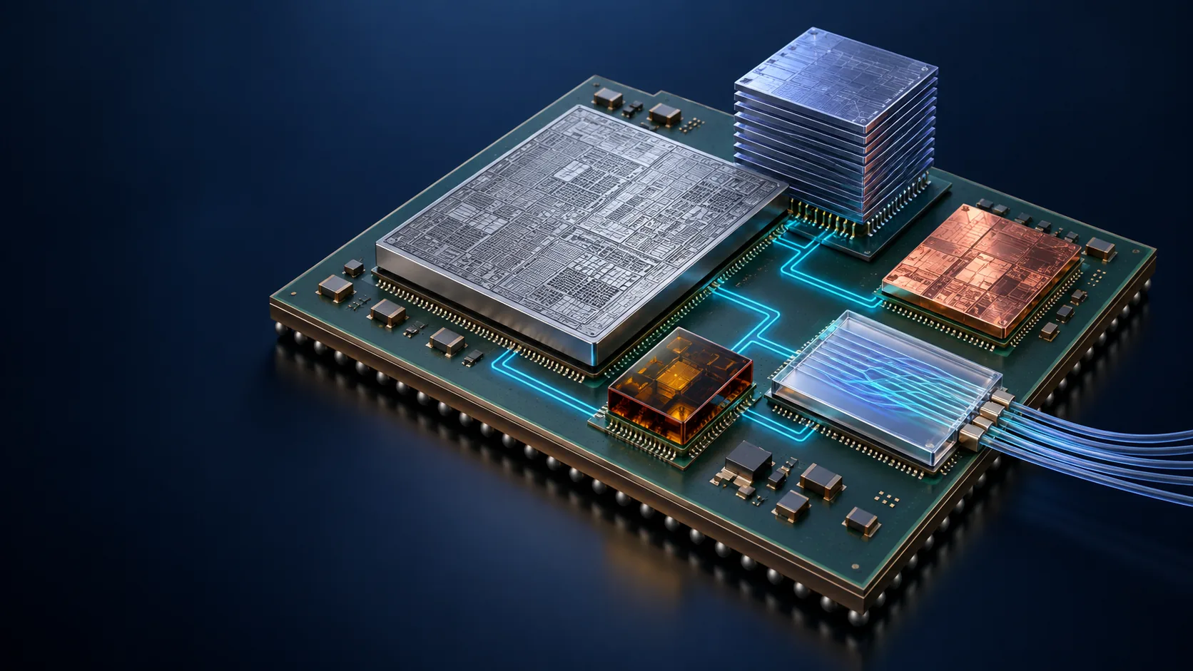
The term is often used interchangeably with "chiplets", but it covers a wider field — and from a materials standpoint, a far harder one. This article looks at what it actually means to put compound semiconductors, and light itself, into the same package as silicon.
- What heterogeneous integration is (the short version)
- How it differs from chiplets — two terms that get conflated
- "Different" comes in four degrees
- Case 1: putting compound semiconductors on silicon (imec)
- Case 2: electronics and photonics in one stack (TSMC COUPE)
- A materials engineer's view: three mismatches
- What eight years did to bonding accuracy
- What is still hard
- Glossary / Primary sources / Claim-to-source audit
Sourced = a value stated in published material from a research institute, standards body or manufacturer (link given)
Our calculation = a figure this article derived, with the assumptions spelled out
Not yet confirmed = a plan or target with no confirmed production record
1. What heterogeneous integration is (the short version)
Heterogeneous integration has a definition the industry actually refers to. The Heterogeneous Integration Roadmap (HIR), led by the IEEE Electronics Packaging Society (EPS), puts it this waySourced.
"Heterogeneous Integration refers to the integration of separately manufactured components into a higher-level assembly that, in the aggregate, provides enhanced functionality and improved operating characteristics." (IEEE EPS, Heterogeneous Integration Roadmap)
Three things in that sentence do the work.
- Separately manufactured: these parts were not made together, in one plant, in one process flow.
- Into a higher-level assembly: the package is where they become one thing.
- In the aggregate: the goal is more than the sum of the parts.
The HIR is supported jointly by IEEE EPS, SEMI, the IEEE Electron Devices Society (EDS), the IEEE Photonics Society and the ASME EPPD, and it sets out packaging, test and interconnect technology requirements over a 15-year horizon (25 years for emerging research areas)Sourced. Its stated mission is to identify technical challenges with enough lead time that they do not become barriers to progressSourced.
2. How it differs from chiplets — two terms that get conflated
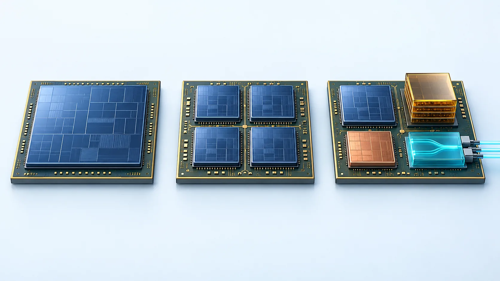
The two words are often used as if they meant the same thing. In fact they point in opposite directions.
| Chiplets | Heterogeneous integration | |
|---|---|---|
| Direction of thought | Dividing | Combining |
| Starting point | A chip that has grown too large to build as one piece | Functions or materials that cannot be built as one piece at all |
| Main motivation | Yield, reticle limit, cost | Capability that a single die cannot deliver, or cannot deliver economically |
| Typical example | Splitting a compute die into several | Putting compound semiconductors or photonic devices onto silicon |
| Relationship | Chiplets are one form of heterogeneous integration, not a separate thing | |
The programme manager of imec's 3D system integration programme told SEMI that "we see heterogeneous integration as a scaling booster for functional partitioning, and as a way to create systems that would be impossible, or economically unviable, as a single chip"Sourced (SEMI, 2 October 2018).
"Impossible as a single chip" is the dividing line. Chiplets split up something that could, in principle, be made as one die. Heterogeneous integration deals with things that could never have been one die in the first place.
3. "Different" comes in four degrees
"Heterogeneous" covers a wide range. How hard the job is depends entirely on what is different and by how much. Re-sorting the technologies this series has covered along that axis makes the landscape much clearer.
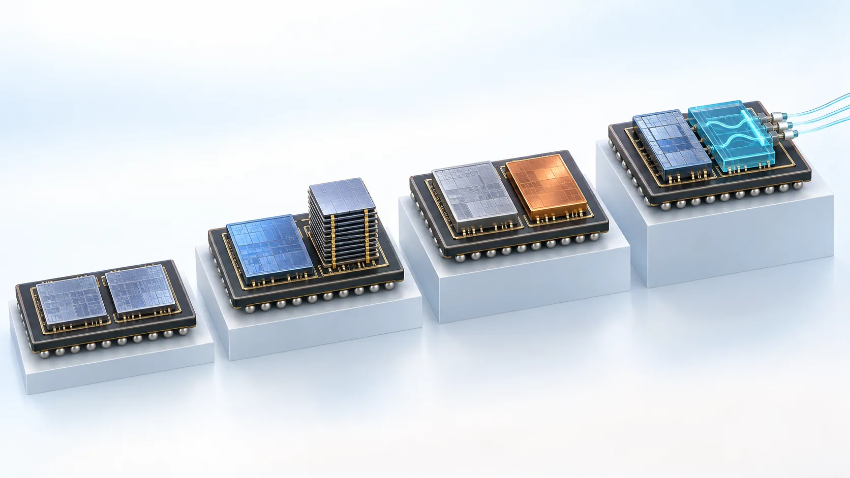
Levels 1 and 2 are silicon meeting silicon. Thermal expansion, cleaning chemistries and handling know-how are shared. At levels 3 and 4, the materials themselves differ. That is where "heterogeneous" starts meaning what it says.
4. Case 1: putting compound semiconductors on silicon (imec)
On 11 June 2026, imec announced a 300 mm RF silicon interposer platform that combines III-V materials such as InP, GaAs and GaN with the scalability and cost efficiency of Si-CMOS technologySourced (imec).
Silicon is not good at everything. Amplification at millimetre-wave and sub-THz frequencies, and emitting light, are things III-V semiconductors such as InP and GaAs do well. High volume, low cost and large-scale integration, meanwhile, belong to silicon. The idea is to combine each material where it is strongest, inside one package.
The three building blocks as published
| Element | What was published |
|---|---|
| High-density embedded capacitors | A new MIMCAP structure gives 10 to 100 times the capacitance density of typical on-chip capacitors in III-V technology, pairing high-k aluminium hafnium oxide with a 3D oxide stud structure in the BEOL |
| Passive component modelling | A framework validated to roughly 300 GHz (sub-THz), able to predict circuit performance accurately when geometry changes |
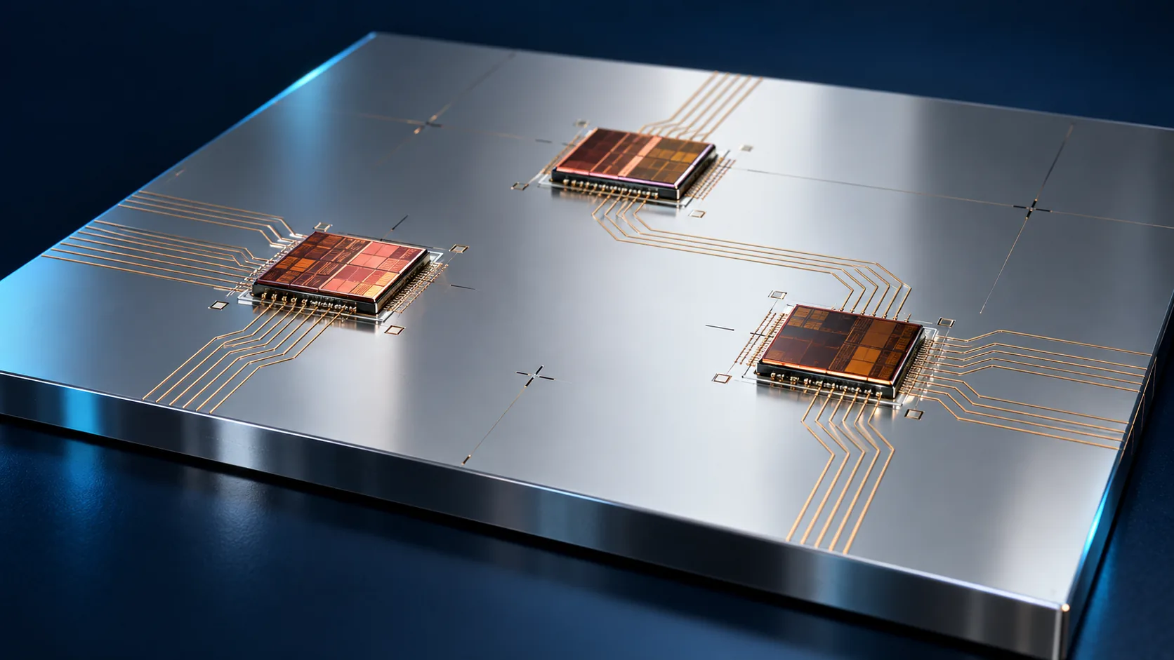
| Laser-assisted bonding | Alignment accuracy below 600 nm and rotational misalignment below 0.05 degrees across 43 devices, while holding reflection below -15 dB in the 110 to 170 GHz band |
All rows Sourced (imec announcement, 11 June 2026). These are results from a research platform and do not represent production-level figures.
Look at how the metric is framed: rotational misalignment below 0.05 degrees across 43 devices. Translational placement error (600 nm) is reported separately from rotation.
That split is specific to high-frequency circuits. At millimetre-wave and sub-THz frequencies, small differences in conductor length or relative angle turn directly into performance spread. What matters is not whether the joint is connected, but how precisely it was placed and oriented — bonding has stopped being a mechanical step and become a step that builds the electrical characteristics.
5. Case 2: electronics and photonics in one stack (TSMC COUPE)
One level harder is putting two different kinds of physics — electrical and optical — into the same package.
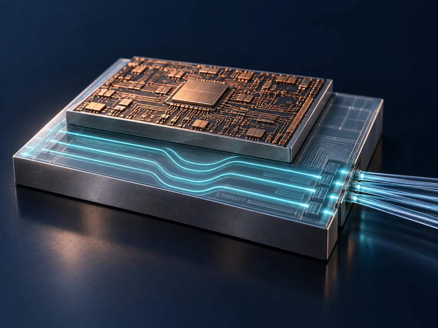
TSMC's COUPE (COmpact Universal Photonic Engine) uses SoIC-X die-stacking technology to stack an electrical die on top of a photonic dieSourced. TSMC states that this arrangement achieves the lowest impedance at the die-to-die interface and delivers better energy efficiency than conventional stacking approachesSourced (TSMC, 24 April 2024).
The timeline is published too: qualification for small pluggables in 2025, and integration into CoWoS in 2026 as co-packaged optics (CPO), bringing optical connectivity inside the packageSourced.
TSMC's technical paper says of COUPE that "for both grating coupler and edge coupler, the structure is solid without any cavity or mechanically weak region, and therefore can achieve low insertion loss without contamination or mechanical concerns"Sourced (TSMC Research, 2021).
Optical components are sometimes built with a cavity so that light has a clear path. But a cavity is a mechanical weak point and a place for contamination to collect. The structure that serves the optics undermines the reliability of the assembly — and that sentence is TSMC saying it sidestepped the conflict by building solid. In heterogeneous integration, the logic of performance and the logic of assembly collide constantly.
6. A materials engineer's view: three mismatches
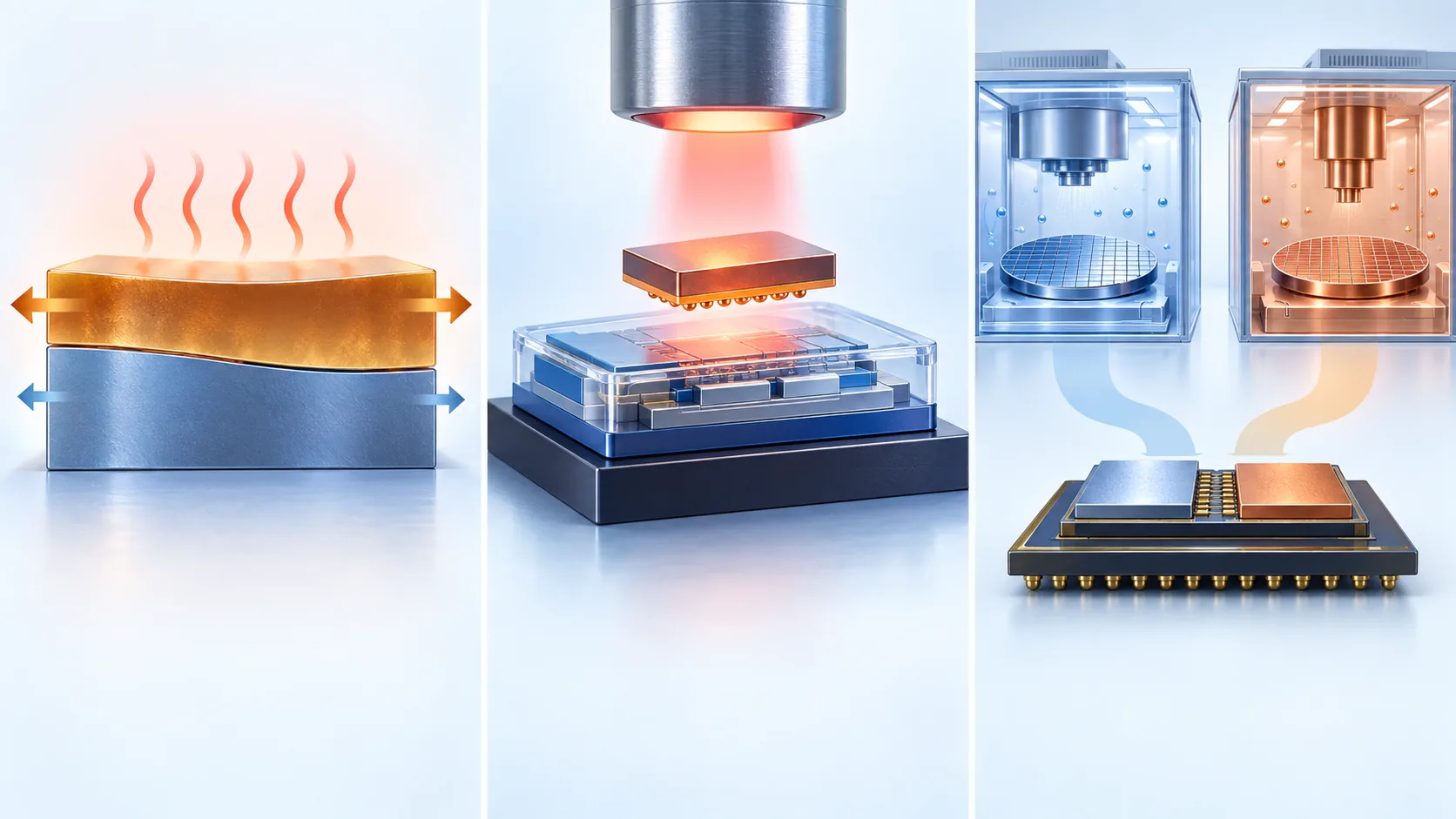
Seen from the materials side, everything that makes heterogeneous integration hard reduces to three mismatches.
The materials SEMI and imec single out
In the SEMI interview quoted earlier, imec's programme manager said that heterogeneous integration is pushing materials to their limits, and named these specificallySourced:
- TBM (temporary bond materials) — adhesives that hold a thin die for handling and then release it
- WLUF (wafer-level underfill)
- Photosensitive polymers for fine line and space (covered in the RDL article)
On die-to-wafer assembly, the same interview said that reaching pitches well below 10 µm remained a challenge in terms of alignment and cleanlinessSourced. That statement dates from 2018. The next section looks at what happened afterwards.
7. What eight years did to bonding accuracy
Whether heterogeneous integration moves from concept to product depends on how accurately unlike things can be placed. Laying the published numbers out in order makes the trajectory visible.
The three numbers come from different technologies measured under different conditions (D2W hybrid bonding and laser-assisted bonding are not the same joining method). This is not a like-for-like comparison. Treat it as an illustration that demonstrations are now reaching territory once described as a challenge.
8. What is still hard
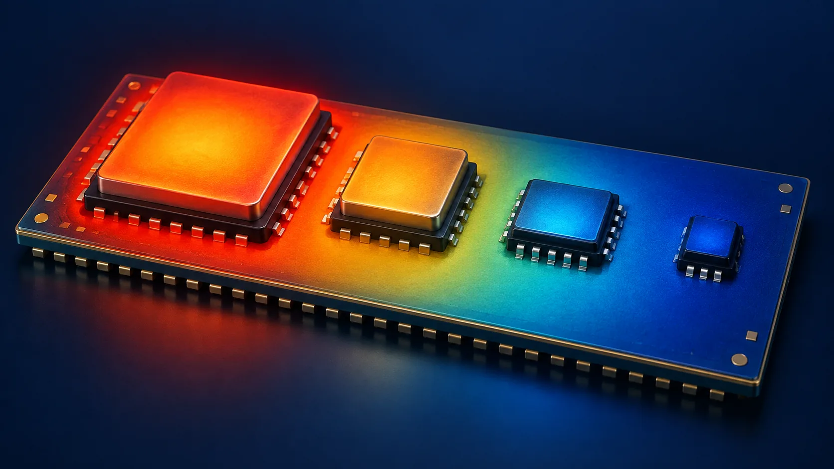
(1) Heat — parts with very different power densities share one lid
In heterogeneous integration, components with different power consumption and different thermal behaviour end up in one enclosure. The compute die runs hot, photonic devices are sensitive to temperature change, and compound semiconductors have their own temperature characteristics. One cooling design has to satisfy all of them, and that is getting harder.
(2) Design — which function belongs on which layer
Design was the first item raised in the SEMI interview: "if you break up a large chip you have to decide how to reassemble it, and which function belongs at which level of the hierarchy. We would like to do that with a tool set that supports the designer, rather than by hand"Sourced.
(3) Test
Once you are gathering parts made in different plants and assembling them, the advantage disappears unless every part can be confirmed good before assembly. And screening a photonic or high-frequency device needs different equipment from screening logic.
9. Glossary
- Heterogeneous integration
- Integrating separately manufactured components into a higher-level assembly that, in the aggregate, improves function and operating characteristics.
- HIR
- Heterogeneous Integration Roadmap. An industry roadmap led by IEEE EPS and partners.
- Monolithic
- Building every function into a single piece of silicon. The opposite of heterogeneous integration.
- III-V semiconductors
- InP, GaAs, GaN and similar. Strong at high-frequency operation and light emission, where silicon is weak.
- InP
- Indium phosphide. Used for light-emitting and light-detecting devices in optical communication.
- GaN
- Gallium nitride. Used in high-frequency and high-power devices.
- MIMCAP
- Metal-insulator-metal capacitor. A capacitor built into the interconnect layers.
- high-k
- An insulator with high permittivity, used to get large capacitance from a small area.
- BEOL
- Back End Of Line. The wiring steps that follow transistor formation.
- Laser-assisted bonding
- Joining by heating locally with a laser, which limits the thermal load on everything nearby.
- Silicon photonics
- Building optical circuits on silicon.
- CPO
- Co-Packaged Optics. Optical components housed in the same package as the processor.
- EIC / PIC
- Electronic integrated circuit / photonic integrated circuit. COUPE stacks one on the other.
- Grating coupler / edge coupler
- Two ways of connecting an optical fibre to a waveguide on the chip.
- Insertion loss
- Signal lost in passing through a component. Lower is better.
- TBM
- Temporary Bond Material. An adhesive used to hold a thin die during handling.
- WLUF
- Wafer Level UnderFill. Underfill applied while still at wafer level.
10. Primary sources
- IEEE EPS "Heterogeneous Integration Roadmap" — eps.ieee.org
- imec "imec unlocks system-level III-V chiplet integration on Si-CMOS, advancing its 300mm RF silicon interposer", 11 June 2026 — imec-int.com
- imec "imec demonstrates die-to-wafer hybrid bonding with Cu interconnect pad pitch of 2um", 29 May 2024 — imec-int.com
- SEMI "3D Heterogeneous Integration Drives Demand for New Materials and Integration Solutions", 2 October 2018 (interview with Gerald Beyer of imec) — semi.org
- TSMC "TSMC Celebrates 30th North America Technology Symposium", 24 April 2024 (includes the COUPE description) — pr.tsmc.com
- TSMC Research "Heterogeneous Integration of a Compact Universal Photonic Engine for Silicon Photonics Applications in HPC", 2021 — research.tsmc.com
- TSMC CoWoS technology page — 3dfabric.tsmc.com
11. Claim-to-source audit
| Claim in the text | Basis | Label |
|---|---|---|
| The definition of heterogeneous integration: integrating separately manufactured components into a higher-level assembly that in the aggregate provides enhanced functionality and improved operating characteristics | IEEE EPS / HIR[Source 1] https://eps.ieee.org/technology/heterogeneous-integration-roadmap/ | Sourced |
| The HIR is supported by IEEE EPS, SEMI, IEEE EDS, the IEEE Photonics Society and ASME EPPD; it sets out packaging, test and interconnect requirements over 15 years (25 for emerging areas); its mission is to identify challenges before they become barriers | IEEE EPS / HIR[Source 1] https://eps.ieee.org/technology/heterogeneous-integration-roadmap/ | Sourced |
| imec: heterogeneous integration is a scaling booster for functional partitioning and a way to create systems that would be impossible or economically unviable as a single chip | SEMI interview, 2 October 2018[Source 4] https://www.semi.org/en/blogs/technology-trends/materials-and-processes-for-3d-heterogeneous-integration | Sourced |
| imec: a 300 mm RF silicon interposer combining III-V (InP, GaAs, GaN) with Si-CMOS; MIMCAP giving 10 to 100 times the capacitance density using high-k aluminium hafnium oxide with a 3D oxide stud; modelling validated to about 300 GHz; laser-assisted bonding with alignment below 600 nm, rotational misalignment below 0.05 degrees across 43 devices, and reflection below -15 dB in the 110 to 170 GHz band | imec press release, 11 June 2026[Source 2] https://www.imec-int.com/en/press/imec-unlocks-system-level-iii-v-chiplet-integration-si-cmos-advancing-its-300mm-rf-silicon | Sourced |
| TSMC COUPE: SoIC-X used to stack an electrical die on a photonic die; lowest impedance at the die-to-die interface and better energy efficiency than conventional stacking; qualification for pluggables in 2025 and integration into CoWoS as CPO in 2026 | TSMC press release, 24 April 2024[Source 5] https://pr.tsmc.com/english/news/3136 | Sourced |
| COUPE uses a solid structure with no cavity or mechanically weak region, for both grating and edge couplers, achieving low insertion loss without contamination or mechanical concerns | TSMC Research paper, 2021[Source 6] https://research.tsmc.com/page/on-chip-interconnect/14.html | Sourced |
| TBM, WLUF and photosensitive polymers for fine line and space are being pushed to their limits; die-to-wafer pitches well below 10 um were not yet reached on alignment and cleanliness grounds as of 2018; the wish to support design with a tool set rather than by hand | SEMI interview, 2 October 2018[Source 4] https://www.semi.org/en/blogs/technology-trends/materials-and-processes-for-3d-heterogeneous-integration | Sourced |
| imec D2W hybrid bonding at 2 um pitch, overlay below 350 nm, using plasma dicing | imec press release, 29 May 2024[Source 3] https://www.imec-int.com/en/press/imec-demonstrates-die-wafer-hybrid-bonding-cu-interconnect-pad-pitch-2mm | Sourced |
| The four degrees of "different" used to organise section 3 | Commentary by this article. Not a standardised industry classification | Commentary |
| The three mismatches (thermal expansion, process temperature, contamination control); the point that rotational accuracy drives high-frequency performance; the point that differing thermal behaviour complicates cooling design | Commentary based on general relationships in materials engineering and process integration. No numerical claim is made about any specific product | Commentary |
| The three values in Fig. 6 are not a like-for-like comparison | Stated in the text and the figure note, because the sources differ in technology and measurement conditions. This article's own caveat | Commentary |
Last updated 20 September 2026. Sources are limited to primary material (official announcements and technical publications from standards bodies, research institutes and manufacturers). All figures are explanatory concept graphics. Visual-overview figures are shown as AI-generated conceptual images, matching the Japanese edition. Vector drawings are retained where they carry quantitative values or precision-critical technical labels. AI-generated images do not depict real equipment, products, facilities, dimensions or exact cross-sections; replaced source SVG overview drawings remain in the HTML but are hidden.