COMPANY PROFILE / SEMICONDUCTOR BACK-END
AMD
The company that first took "split the chip up and reassemble it" into volume production
Like NVIDIA, AMD is a design house with no factories of its own. Its distance from the back end, however, is visibly shorter. It discloses that it holds a 15% stake in its back-end contractors and paid those joint ventures US$2bn in 2025. Stop building one large chip, and instead line up small chips, chiplets, and reassemble them inside a single package: this profile follows how the first company to put that idea into volume production in a mainstream CPU relates to the back end, using only published figures.
- AMD in 30 seconds
- The logo and how the name is written
- What the company actually does: the chiplet idea
- Scale: five years of revenue
- Company category and position in the back-end industry
- Sites and the countries where it manufactures
- Leading products and share in semiconductor back-end work
- Current investment plans
- Major corporate partners
- Where the company is heading in this field
- The risks this company carries
- Glossary, references and claim-to-source audit
1. AMD in 30 seconds
(NASDAQ Global Select Market)Ticker AMD. 1,630.41m shares outstanding as of 30 January 2026
(US$34,639m)Up 34% year on year. The fiscal year ends on the last Saturday of December; this one closed on 27 December 2025
(fabless semiconductor)But with a 15% stake in back-end joint ventures
AMD is not a back-end specialist. It nevertheless appears in every account of the semiconductor back end, for two reasons.
The first is technology. In its 10-K the company describes its own strength as leadership in design, integration and advanced packaging, and lists investment in customisable chiplet platforms Sourced. This is the company that took the idea of winning performance by splitting and reassembling, rather than by shrinking, into volume production in a flagship product.
The second is ownership. AMD holds 15% of two joint ventures formed with affiliates of Tongfu Microelectronics, a Chinese back-end company, and discloses in hard numbers that it paid those joint ventures US$2bn in 2025 Sourced. It is very rare for a design house to put a figure on what it spends on back-end work. AMD is one of the few design companies whose back-end cost is visible as a number, and that is what makes this profile worth reading.
2. The logo and how the name is written

The AMD logo, the arrow-shaped symbol known as the AMD Arrow logo together with the wordmark, is a registered trademark of the company. The 10-K states as much: AMD, the AMD Arrow logo, 3D V-Cache, EPYC, Infinity Fabric, AMD Instinct, Radeon, Ryzen and the rest are trademarks of Advanced Micro Devices, Inc. Sourced.
A note on style: the legal name in statutory documents is Advanced Micro Devices, Inc., but every product and brand carries the AMD prefix, as in AMD Ryzen, AMD EPYC and AMD Instinct.
Official site: https://www.amd.com/en.html3. What the company actually does: the chiplet idea
AMD designs CPUs, GPUs and FPGAs and contracts out the manufacturing. It is fabless. What it designs, though, connects directly to the back end.
What a chiplet is
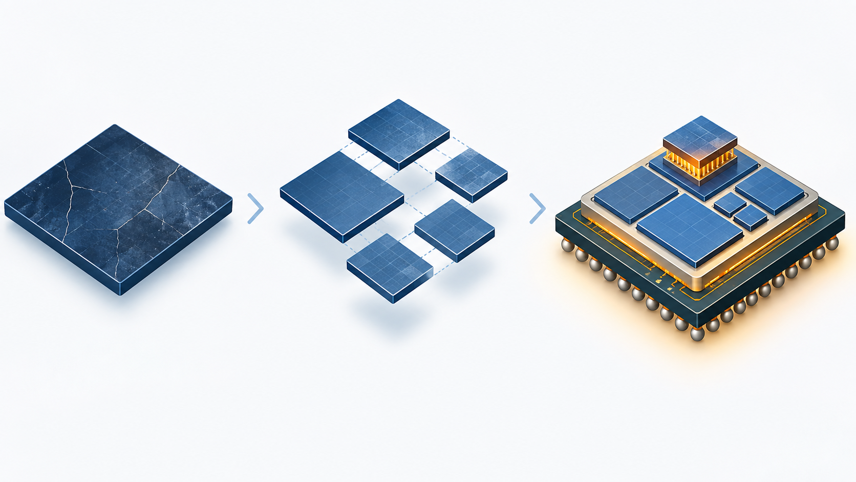
For decades semiconductors advanced by packing every function onto a single piece of silicon. But the larger a die grows, the more sharply the probability of getting a good one out of a wafer, the yield, falls away. AMD's answer was to build a small chip for each function separately and reassemble them later inside the package. Those small chips are the chiplets.
If everything is on one die, the back end only has to dice it, mount it on a substrate and encapsulate it. Once several chiplets have to share one package, though, how the dies are wired to each other, how they are laid out and how they are cooled all have to be solved inside the package. In other words, part of the design that determines performance has moved from the front end to the back end. That is why AMD lists design, integration and advanced packaging together as its strengths in the 10-K Sourced.
The best-known implementation is 3D V-Cache. The CPU's cache memory is built as a separate die and stacked on top of the compute die, and the Ryzen 9 9950X3D and 9900X3D launched in 2025 use second-generation 3D V-Cache Sourced. Rather than sit side by side in two dimensions, the pieces stack in three, physically shortening the distance between core and cache.
The business is reported in three segments Sourced.
| Segment | Contents | FY2025 revenue | Operating income |
|---|---|---|---|
| Data Center | AI accelerators (AMD Instinct), server CPUs (EPYC), GPUs, DPUs, AI NICs and FPGAs | US$16,635m | US$3,603m |
| Client and Gaming | Desktop and notebook CPUs and APUs (Ryzen), discrete GPUs (Radeon), semi-custom SoCs for games consoles | US$14,550m | US$2,855m |
| Embedded | FPGAs, adaptive SoCs and System-on-Modules for industrial, automotive, medical and communications use | US$3,454m | US$1,243m |
| Total | - | US$34,639m | US$3,694m |
Total operating income (US$3,694m) is stated after deducting costs not allocated to the segments (All other, minus US$4,007m). From the first quarter of FY2025 the former Client and Gaming segments were merged into one.
There is a sentence in AMD's 10-K that no one on the materials side should skip. The company may purchase equipment, materials and substrates from multiple suppliers for use by its back-end manufacturing service providers Sourced.
Normally it is the OSAT that buys the encapsulant and the substrate used in back-end work. AMD, however, has written into a statutory filing that it sometimes procures the materials its back-end partners will use. Its risk factors add that as products grow more technically complex, dependence on those third parties increases. For a materials maker the implication is that the design house, not only the OSAT, can be the direct counterparty. Nothing of this kind appears in NVIDIA's 10-K, fabless though it also is. The more a company relies on chiplets in volume, the further upstream into procurement it reaches, and the disclosures show it.
4. Scale: five years of revenue
| Fiscal year | Revenue (US$m) | R&D expense (US$m) | Operating income (US$m) | Capital spending (US$m) |
|---|---|---|---|---|
| FY2021 | 16,434 | 2,845 | 3,648 | 301 |
| FY2022 | 23,601 | 5,005 | 1,264 | 450 |
| FY2023 | 22,680 | 5,872 | 401 | 546 |
| FY2024 | 25,785 | 6,456 | 1,900 | 636 |
| FY2025 | 34,639 | 8,091 | 3,694 | 974 |
Operating income sagged in 2022 and 2023 because amortisation of the intangibles acquired with Xilinx ran at over US$1bn a year. FY2025 net income was US$4,335m and gross margin was 50%.
Being fabless keeps capital spending small
Capital spending in FY2025 was US$974m, or 2.8% of revenue Our calculation. Property and equipment, net, came to only US$2,312m. The split by country is as follows Sourced.
| Country | End of FY2025 (US$m) | End of FY2024 (US$m) | Share |
|---|---|---|---|
| United States | 1,717 | 1,312 | 74.3% Our calculation |
| Singapore | 157 | 140 | 6.8% Our calculation |
| Canada | 142 | 104 | 6.1% Our calculation |
| Other | 296 | 246 | 12.8% Our calculation |
| Total | 2,312 | 1,802 | 100% |
In contrast to NVIDIA, which holds 31% of its property and equipment in Taiwan, roughly three quarters of AMD's assets are in the United States. Taiwan is not broken out separately.
5. Company category and position in the back-end industry
The category is manufacturer, specifically a fabless semiconductor company. Its position in the back-end industry, though, differs a little from NVIDIA's purely as-a-buyer stance, because AMD is also a shareholder, and sometimes a buyer of materials.
For the avoidance of doubt, AMD has no back-end revenue, because it sells no back-end service. The bottom row of Fig. 2 is not revenue but the opposite, money AMD paid out. Note 7 does, however, record equity-method income from those joint ventures, US$26m in FY2025, so AMD takes a small share of back-end profits into its own accounts Sourced. That is an unusual structure for a design company.
6. Sites and the countries where it manufactures
AMD owns no production plants either. The "Properties" section of the 10-K says the following Sourced.
| Category | Contents |
|---|---|
| Overall | About 6.8 million square feet used for research, engineering, administration and warehousing, of which about 5.4 million square feet is leased and about 1.4 million square feet owned |
| Headquarters | Santa Clara, California |
| Main sites | Austin, Texas; San Jose, California; Shanghai, China; Markham, Ontario, Canada; Longmont, Colorado; Dublin, Ireland; Singapore; Bangalore and Hyderabad, India |
| Manufacturing sites | None listed, because the company holds none |
So where are the products actually built? The 10-K describes it step by step Sourced.
| Step | Contractor (named in the 10-K) | Location |
|---|---|---|
| Wafer fabrication (front end) | TSMC (for HPC, FPGA and adaptive SoC products), GLOBALFOUNDRIES (12nm and 14nm HPC products), UMC and Samsung (programmable logic) | The company states that it depends on third-party foundries in the United States, Europe and Asia |
| Assembly, test, mark and packaging (ATMP) | Two joint ventures with affiliates of Tongfu Microelectronics, plus SPIL (Siliconware Precision Industries) and KYEC (King Yuan Electronics) | Substantially all product assembly and final test is performed at third-party facilities in China, Malaysia and Taiwan |
| Board assembly (graphics cards and similar) | Third-party contract manufacturers, not named | Not stated |
The most practically useful thing in that table is that the front-end and back-end maps do not match. Wafers are built in Taiwan, the United States and Europe, but assembly and test happen in China, Malaysia and Taiwan, and most of the ATMP work goes through joint ventures with a Chinese company. In other words, the actual delivery addresses for encapsulant, substrate and underfill lean towards China and Malaysia. Geopolitical discussion tends to concentrate on the front end and Taiwan, yet for AMD products specifically, the back end carries the heavier exposure to China. AMD says as much itself, noting in its risk factors that geopolitical change between China and Taiwan could disrupt the operations of the Taiwan-based third-party foundries, manufacturing facilities and subcontractors it relies on Sourced.
7. Leading products and share in semiconductor back-end work
No back-end product, but technology and an equity stake
AMD sells no back-end service either, so it has no leading back-end product and no share. Five things can be stated with confidence from primary sources.
- It names design, integration and advanced packaging as its own strengths, stated in the business overview of the 10-K Sourced
- It is investing in customisable chiplet platforms and in AMD Infinity Fabric switches Sourced
- It shipped products with second-generation 3D V-Cache in 2025, the Ryzen 9 9950X3D and 9900X3D Sourced
- It holds 15% of two back-end joint ventures and accounts for them by the equity method, with a carrying value of US$176m Sourced
- It paid those joint ventures US$2.0bn in FY2025 and US$1.7bn in FY2024, with US$408m still payable Sourced
| Disclosure on the ATMP joint ventures | FY2025 | FY2024 |
|---|---|---|
| AMD's ownership interest | 15% | 15% |
| Carrying value of the investment | US$176m | US$149m |
| Purchases by AMD, that is, what AMD paid | US$2,000m | US$1,700m |
| Amounts payable at year end | US$408m | US$476m |
| Equity-method income | US$26m | US$33m |
The company states that the majority of its ATMP services are provided by these joint ventures. The US$2,000m is therefore not the whole of AMD's back-end spending but the majority of it Our calculation. The company also states that it has no obligation to fund the joint ventures further.
How much of the back-end market AMD's chiplets and 3D V-Cache account for cannot be established from primary sources. Nor does the 10-K say which bonding technique is used to stack 3D V-Cache, hybrid bonding or otherwise Not yet confirmed. Claims of the form "AMD's hybrid bonding runs on equipment from company X" cannot be supported from AMD's statutory filings and are not used here.
Likewise, AMD's 10-K says nothing about whether it uses CoWoS, in contrast to NVIDIA, which states its use of CoWoS explicitly Not yet confirmed.
8. Current investment plans
AMD has no plan to invest in factories either. What is disclosed are purchase commitments.
The 10-Q puts it this way: the company's contractual obligations and purchase commitments relate primarily to obligations to purchase wafers, substrates and components from third parties Sourced. Substrates are named alongside wafers as the subject of those commitments. The package substrate is being treated, in procurement terms, as the equal of the wafer, and for anyone working on back-end materials that is an important piece of primary evidence. In the FY2025 10-K the same sentence read "wafers and substrates"; "components" was added in the second quarter of FY2026 Our calculation.
Investment also goes into acquisitions rather than equipment. The main moves in FY2025 were these Sourced.
| Date | Substance | Amount |
|---|---|---|
| 31 March 2025 | Acquired ZT Group Int'l (ZT Systems), a supplier of AI and general-purpose compute infrastructure, for its design intellectual property and people | US$4,400m |
| October 2025 | Sold ZT's data centre infrastructure manufacturing business to Sanmina, keeping the design side and letting the manufacturing go | US$1,356m proceeds |
| During 2025 | Several acquisitions aimed at strengthening software capability, adding co-packaged optics and acquiring high-speed inference technology | Individual amounts not disclosed |
Buying ZT's manufacturing arm and selling it within months reads as confirmation that AMD intends to stay out of manufacturing. Investing in co-packaged optics, by contrast, moves optical components inside the package, which widens the territory the back end has to cover.
9. Major corporate partners
| Kind | Counterparty | Substance | Primary source |
|---|---|---|---|
| Equity (joint venture) | Affiliates of Tongfu Microelectronics | Two joint ventures for ATMP work, that is, assembly, test, mark and packaging. AMD holds 15% and applies the equity method. FY2025 purchases were US$2.0bn | Stated in Note 7 to the 10-K Sourced |
| Manufacturing contract | TSMC, GLOBALFOUNDRIES, UMC, Samsung Electronics | Wafer fabrication. A wafer supply agreement with GF sets minimum annual capacity and pricing through 2026 | Stated in the 10-K Sourced |
| Back-end contract | SPIL (Siliconware Precision Industries), KYEC (King Yuan Electronics) | Providers of ATMP services, named alongside the two joint ventures | Stated in the 10-K Sourced |
| Customer agreement | OpenAI OpCo, LLC | A product purchase agreement signed in October 2025 covering 6 gigawatts of AMD GPUs, the first gigawatt being AMD Instinct MI450 series parts | Stated in the 10-K Sourced |
| Divestment buyer | Sanmina Corporation | Bought ZT's data centre infrastructure manufacturing business in October 2025 | Stated in the 10-K Sourced |
AMD writes that it may itself buy the equipment, materials and substrates its back-end providers use, but it names neither the suppliers nor the amounts Not yet confirmed. Specific supplier names for ABF film, encapsulation resin or package substrates cannot be confirmed from AMD's primary material and are not used here.
10. Where the company is heading in this field
Anything said here is a forecast, so the established facts and the outlook drawn from them are kept apart.
What is established
| Fact | What it implies for the back end |
|---|---|
| Purchase commitments rose from US$12.2bn to US$30.3bn in six months | Volumes are climbing fast, and the fact that substrates are named alongside wafers ties this directly to the back end |
| Data centre revenue is 48.0% of the total, up 32% year on year | The domain that needs advanced packaging has become the main business |
| Payments to the ATMP joint ventures rose from US$1.7bn to US$2.0bn | Back-end spending is rising steadily, though not as fast as revenue at 34% |
| A 6-gigawatt product purchase agreement was signed with OpenAI | It underpins shipment volumes for several years, which feeds through to back-end utilisation |
| Co-packaged optics technology was acquired | Optical components are moving into the package, widening the materials and process scope of the back end |
| ZT's manufacturing business was sold immediately after being acquired | The policy of not owning manufacturing is intact |
Outlook
Not yet confirmed Read plainly, the facts above suggest AMD will remain, for the back-end industry, a smaller counterparty than NVIDIA but a more deeply involved one. Revenue is about one sixth of NVIDIA's, yet AMD holds equity in back-end companies, sometimes buys the materials itself, and invests in things like co-packaged optics that extend what the back end has to do. Measured purely by order volume it is a small customer; measured by the technical demands it places, it carries real weight.
Not yet confirmed The largest uncertainty is geopolitics. A structure in which the majority of ATMP work depends on joint ventures with a Chinese company may have to be revisited if controls between the United States and China tighten. AMD itself writes that substantially all assembly and final test is concentrated in China, Malaysia and Taiwan, which shows an awareness of the need to spread the risk, but no relocation plan appears in either the 10-K or the 10-Q.
11. The risks this company carries
What follows is drawn from the risk factors AMD sets out in its own statutory filings, narrowed to those that matter in a back-end context Sourced.
| Risk | Substance | Supporting figures |
|---|---|---|
| Reliance on one back-end provider | The company states that the majority of its ATMP services come from the ATMP joint ventures and that there is no assurance they can meet its long-term requirements. Late supply would mean lost orders | FY2025 payments of US$2.0bn, with US$408m still payable |
| Geographic concentration of the back end | Substantially all assembly and final test sits in China, Malaysia and Taiwan. The filing says geopolitical change between China and Taiwan could disrupt operations | Stated in the risk factors of the 10-K |
| Sourcing materials and substrates | Inability to obtain equipment, materials or substrates is listed as a risk in its own right. The filing also notes an industry-wide shortage of memory and rising memory prices | Purchase commitments of US$30.3bn as of June 2026 |
| Export controls | Charges were taken on inventory and related items in connection with U.S. export controls on AMD Instinct MI308 | About US$440m in FY2025, recorded in cost of revenue |
| Yield | The filing states that yield is a function of product design, process technology and packaging technology, and that packaging technology is typically proprietary to the manufacturer. AMD cannot control yield directly | Stated in the risk factors of the 10-K |
| Customer skew | No customer reached 10% of revenue in FY2025 or FY2024, but one accounted for about 11% of receivables. In FY2023 one customer was 18% of revenue | Stated in the notes to the 10-K |
One sentence in the risk factors is particularly telling for anyone working with back-end materials. Semiconductor yield is a function of product design, process technology and packaging technology, and packaging technology is typically proprietary to the manufacturer Sourced.
AMD is saying that while it decides the design, meaning the chiplet arrangement, the packaging technology that realises it is held by the ATMP side. From a materials maker's seat that structure is easier to work with than it looks, because it tells you who to pitch to. Layout and thermal requirements come down from AMD, but the authority to select the actual materials most likely sits with the ATMP providers, the joint ventures, SPIL and KYEC. AMD's statement that it sometimes buys the materials its back-end partners use reads as the company acknowledging an exception to that rule.
12. Glossary
- Chiplet
- A small die produced by splitting one large chip up by function. Building them separately and reassembling them in one package improves yield and cost. AMD took the approach into volume production in a flagship CPU.
- 3D V-Cache
- An AMD trademark. The CPU's cache memory is built as a separate die and stacked on top of the compute die. Products launched in 2025 use the second generation.
- ATMP
- Assembly, Test, Mark and Packaging. The term AMD's 10-K uses for back-end work.
- OSAT
- Outsourced Semiconductor Assembly and Test. A company specialising in contract back-end work. AMD's 10-K calls them ATMP partners or subcontractors.
- Equity method
- The accounting treatment used when an investor has significant influence over an investee. A share of the investee's profit is taken into the investor's own accounts. AMD applies it to its 15% holdings in the ATMP joint ventures.
- Substrate
- The board a die is mounted on and wired out through. It is the foundation of the package. AMD names it alongside wafers as a subject of its purchase commitments.
- Co-packaged optics
- Technology that brings optical communication components inside the same package as the chip. AMD acquired a company in this field in 2025.
- Form 10-K and 10-Q
- The annual and quarterly reports a U.S. company files with the Securities and Exchange Commission. They are audited or reviewed and carry legal liability for their contents.
 AI-generated concept
13. References
- AMD Form 10-K for the fiscal year ended 27 December 2025 (filed with the U.S. SEC on 4 February 2026). Revenue, R&D expense, operating income, net income, revenue by segment and by region, headcount, Properties, property and equipment by country, capital spending, the named foundries and ATMP contractors, the ownership interest in and purchases from the ATMP joint ventures, purchase commitments, the ZT Systems acquisition and the sale of its manufacturing business, the OpenAI agreement and risk factors. sec.gov/Archives/edgar/data/2488/000000248826000018/amd-20251227.htm
- AMD Form 10-Q for the quarter ended 27 June 2026 (filed with the U.S. SEC on 5 August 2026). Quarterly and segment revenue, gross margin, unconditional purchase commitments of US$30.3bn and the wording describing what they cover, and the risk factors relating to the ATMP joint ventures. sec.gov/Archives/edgar/data/2488/000000248826000123/amd-20260627.htm
- U.S. SEC EDGAR XBRL company facts API (CIK 0000002488). Revenue, R&D expense, operating income, net income and capital spending for FY2021 to FY2025, as tagged in each year's Form 10-K. data.sec.gov/api/xbrl/companyfacts/CIK0000002488.json
- AMD Official website, used to check how the name is written and the logo. https://www.amd.com/en.html
14. Claim-to-source audit
| Claim in the article | Category | Source |
|---|---|---|
| Legal name, head office address, year founded (1 May 1969), listing (Nasdaq, AMD), shares outstanding | Sourced | Reference 1 sec.gov/.../amd-20251227.htm |
| FY2025 revenue of US$34,639m, up 34%, gross margin 50%, net income US$4,335m | Sourced | Reference 1 sec.gov/.../amd-20251227.htm |
| Revenue, R&D expense, operating income and capital spending for FY2021 to FY2024 | Sourced | Reference 3 data.sec.gov/.../CIK0000002488.json |
| The year-on-year figures in Fig. 1 (+68%, +44%, -3.9%, +14%, +34%) | Our calculation | Derived from the annual revenue in reference 3 data.sec.gov/.../CIK0000002488.json |
| Revenue and operating income by segment (Data Center US$16,635m and the rest) | Sourced | Reference 1 sec.gov/.../amd-20251227.htm |
| Segment shares of revenue (48.0%, 42.0%, 10.0%) and capital spending at 2.8% | Our calculation | Derived from the amounts in reference 1 sec.gov/.../amd-20251227.htm |
| About 31,000 employees, and the floor areas and main sites in Properties | Sourced | Reference 1 sec.gov/.../amd-20251227.htm |
| The ATMP joint ventures: 15% interest, US$176m carrying value, US$2.0bn of purchases, US$408m payable, US$26m equity-method income | Sourced | Reference 1, Note 7 sec.gov/.../amd-20251227.htm |
| US$2,000m being 5.8% of revenue and 12.2% of the US$16,456m cost of revenue | Our calculation | Derived from the amounts in reference 1 sec.gov/.../amd-20251227.htm |
| The named contractors (TSMC, GLOBALFOUNDRIES, UMC, Samsung, the Tongfu joint ventures, SPIL, KYEC) | Sourced | Reference 1 sec.gov/.../amd-20251227.htm |
| Substantially all assembly and final test taking place in China, Malaysia and Taiwan | Sourced | Reference 1 sec.gov/.../amd-20251227.htm |
| The statement that AMD may itself buy equipment, materials and substrates for its back-end providers | Sourced | Reference 1, risk factors sec.gov/.../amd-20251227.htm |
| Property and equipment by country (United States US$1,717m and the rest) and the shares | Our calculation | Shares derived from the amounts in reference 1 sec.gov/.../amd-20251227.htm |
| The products using second-generation 3D V-Cache and the investment in chiplet platforms | Sourced | Reference 1 sec.gov/.../amd-20251227.htm |
| The US$4.4bn ZT Systems acquisition, the sale of its manufacturing business to Sanmina and the 6-gigawatt OpenAI agreement | Sourced | Reference 1 sec.gov/.../amd-20251227.htm |
| The roughly US$440m of charges tied to MI308 export controls, and customer concentration | Sourced | Reference 1 sec.gov/.../amd-20251227.htm |
| Unconditional purchase commitments of US$30.3bn as of 27 June 2026, covering wafers, substrates and components | Sourced | Reference 2 sec.gov/.../amd-20260627.htm |
| The roughly 2.5-fold rise in six months, and the addition of "components" to the wording in FY2026 | Our calculation | Comparison of the wording in references 1 and 2 sec.gov/.../amd-20260627.htm |
| The bonding technique used for 3D V-Cache and the equipment behind it | Not yet confirmed | Absent from the 10-K, so this article makes no estimate |
| Whether AMD uses CoWoS | Not yet confirmed | Absent from AMD's filings, so this article asserts nothing |
| AMD's market share in chiplets or advanced packaging | Not yet confirmed | No primary source exists, so this article states no figure |
| The names of, and amounts paid to, the suppliers of substrates and materials AMD buys | Not yet confirmed | Not disclosed, so this article makes no estimate |
| Whether there is a plan to reduce the back end's reliance on China | Not yet confirmed | Neither the 10-K nor the 10-Q mentions relocation, so this article makes no estimate |
| The outlook in section 10 | Not yet confirmed | An interpretation by this article, drawn from the six items in the facts table |
Last updated 21 September 2026 / Troy Technical
Every figure in this article comes from AMD's statutory filings with the U.S. Securities and Exchange Commission. No research-firm estimates or press-based figures have been used.