COMPANY PROFILE / SEMICONDUCTOR BACK-END
Rapidus
A company with no revenue is producing industry firsts in the back end
Rapidus was founded in 2022 and is aiming at volume production of 2nm logic in the second half of the 2027 financial year. It sells nothing yet and publishes no revenue figure. It nonetheless appears in back-end coverage because its back-end site at Chitose in Hokkaido, RCS, announced what it called an industry first: a prototype RDL interposer built on a 600mm square panel. This profile separates what is settled from what is not, using only the company's own published material.
- Rapidus in 30 seconds
- The logo and how the name is written
- What the company actually does: the integrated RUMS model
- Scale: no revenue is published, so look at the capital instead
- Company category and position in the back-end industry
- Sites and the countries where it operates
- Leading products and share in semiconductor back-end work
- Current investment plans
- Major corporate partners
- Where the company is heading in this field
- The risks this company carries
- Glossary, references and claim-to-source audit
1. Rapidus in 30 seconds
(foundry)But one that intends to carry the back end in house as well
Rapidus has sold nothing yet. Neither revenue nor profit is published, so it cannot be compared with the other companies in this series on the same terms. It comes up in back-end discussion because it has run a NEDO-commissioned project since March 2024 on design and manufacturing technology for chiplet packaging at the 2nm generation, and because the output of that project has been published in concrete form Sourced. Read this profile not as an account of a company with a track record but as an account of what a company is setting out to do.
2. The logo and how the name is written

The Rapidus logo is a trademark of the company. This article reproduces no generated version of it; where the mark is shown, the frame above must hold the genuine logo file taken from the official site.
A note on style: the name is written Rapidus. It is Latin for "fast", which matches the shorter cycle time the company puts at the centre of its proposition. The legal entity is Rapidus Corporation.
Official site: https://www.rapidus.inc/3. What the company actually does: the integrated RUMS model
By its own account Rapidus is a foundry. Unlike a conventional foundry, though, it proposes to provide design support, front-end and back-end work from a single company. It calls this RUMS, Rapid and Unified Manufacturing Service Sourced.
What Rapidus is selling is speed. It says it has adopted a single-wafer process in the front end, handling 300mm wafers one at a time, and that it analyses the resulting data with AI and feeds it back to the design side Sourced. Single-wafer processing is less productive than the usual batch approach, which handles many wafers at once, but it has one advantage: a full history is captured for every individual wafer. From a materials and process development chair this looks like a deliberate trade: buying speed of yield improvement at the price of throughput. That is rational if you assume high mix and low volume; it is hard to sustain on a product that ships in quantity.
4. Scale: no revenue is published, so look at the capital instead
Rapidus is unlisted and has no obligation to file a securities report. Revenue, operating profit and total assets are not published, so five years of revenue cannot be shown Not yet confirmed. What follows instead is the progression of paid-in capital and capital reserve that the company does publish. At present that is the only published number that indicates its size.
| When | Event | Amount | Who provided it |
|---|---|---|---|
| August 2022 | Investment at founding | JPY 7.3bn | Eight companies: Toyota Motor, DENSO, Sony Group, NTT, NEC, SoftBank, Kioxia and MUFG Bank |
| 27 February 2026 | Investment by the Information-technology Promotion Agency (IPA) | JPY 100.0bn | The government, through an incorporated administrative agency under the Ministry of Economy, Trade and Industry |
| 27 February 2026 | A capital increase from 32 private companies | JPY 167.6bn | Canon, the Development Bank of Japan, Fujitsu, NTT, SoftBank, Sony Group and 26 others |
| 5 June 2026 | A further investment by IPA | JPY 150.0bn | The government |
| Total | Paid-in capital and capital reserve | JPY 424.95bn | Of which the government provided JPY 250.0bn (58.8%) and private investors JPY 174.95bn (41.2%) Our calculation |
Headcount is 1,024, as of 1 December 2025. For reference, TSMC employs 90,557 people, which makes Rapidus about one eighty-eighth of its size Our calculation. In scale it is still an organisation in the middle of bringing a single plant up.
5. Company category and position in the back-end industry
The category is a manufacturer, a foundry. It is neither a university nor a government body, yet 58.8% of its capital is government money and its research is funded as a NEDO-commissioned project, so it cannot quite be called a purely private company either Our calculation.
| Measure | A typical OSAT | TSMC | Rapidus |
|---|---|---|---|
| Where the back end sits | It is the business | A value-added service on top of the front end | Part of RUMS, inseparable from the front end |
| Earnings | Earns from contract work | Earns (amount not disclosed) | None yet |
| Size | Tens of thousands of people | 90,557 people | 1,024 people |
| Where the money comes from | Trading profit | Trading profit, bonds and national subsidies | Government equity, private equity and NEDO project funding |
| Scope of the back-end work | A wide range of products | Mainly wafers it made itself | Specialised in 2nm generation chiplets |
6. Sites and the countries where it operates
Sites are in two countries, Japan and the United States Sourced.
| Site | Location | Role |
|---|---|---|
| Tokyo head office | Kojimachi Diamond Building, 4-1 Kojimachi, Chiyoda-ku, Tokyo | Head office functions |
| Chitose office | NTT Chitose Building, 2-16 Chiyoda-cho, Chitose, Hokkaido | Opened January 2024 |
| IIM-1 | 758-62 Bibi, Chitose, Hokkaido | The front-end manufacturing site. Ground was broken in September 2023 and the pilot line began coming up in April 2025 |
| Analysis centre | Adjacent to IIM-1, at Bibi, Chitose, Hokkaido | Physical analysis, environmental chemical analysis, electrical characterisation and reliability testing. Opened 11 April 2026 |
| Rapidus Chiplet Solutions (RCS) | 758-173 Bibi, Chitose, Hokkaido, inside the Seiko Epson Chitose plant | The back-end research and development site. Installation began in October 2024 and full operation started on 11 April 2026 |
| Rapidus Design Solutions | Santa Clara, California, United States | A sales office, established April 2024 |
The address of RCS is inside the Chitose plant of Seiko Epson Corporation Sourced. Rather than put up its own building, Rapidus built a clean room within an existing facility. Equipment installation began in April 2025, the first prototype was announced that December, and full operation started in April 2026. A year and a half from securing a clean room to a prototype is plainly faster than building from bare ground, and the company's talk of shorter cycle times evidently extends to how it assembles the organisation itself. Seiko Epson, incidentally, is one of the 32 companies that took part in the February 2026 capital increase.
7. Leading products and share in semiconductor back-end work
On market share, the conclusion first
Rapidus has neither volume production nor sales, so its share of this field is zero. Nor does it have leading products, in the sense of products on the market Not yet confirmed. What follows is what it has published about the technology it is developing.
Chiplet packaging and the 600mm square panel
Rapidus has said that its back end will use chiplet packaging technology, combining several dies of different function into one package. It offers a forecast that package size will be two to three times larger by 2030 than it is now, and says it will develop 600mm square panel level packaging technology to handle that growth Sourced.
What has been reached so far, as published
| When | Event | What it represents |
|---|---|---|
| March 2024 | Selected for the NEDO project on design and manufacturing technology for chiplet packaging at the 2nm generation | The back-end project begins |
| October 2024 | A back-end research and development site was opened inside the Seiko Epson plant | Installation of RCS begins |
| April 2025 | Installation of production equipment at RCS began | The pilot line is built |
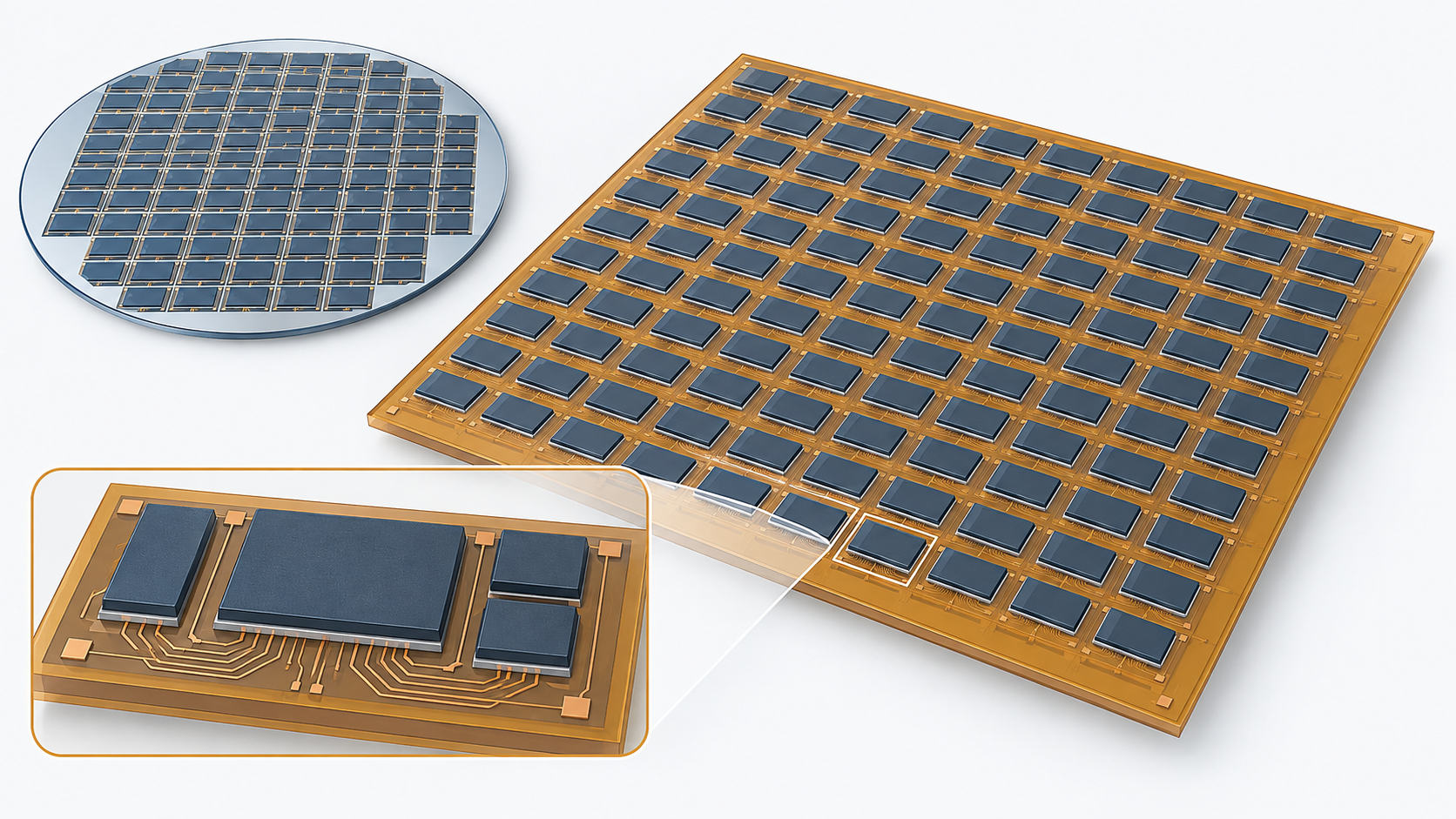
| December 2025 | A prototype organic dielectric RDL interposer on a 600mm square panel, which the company describes as an industry first | A concrete result in the back end |
| 11 April 2026 | RCS and the analysis centre opened and entered full operation | Attended by the Minister of Economy, Trade and Industry, the Governor of Hokkaido and the Mayor of Chitose |
| FY2026 (planned) | Development of 2.xD and 3D package manufacturing technology, and of design and test technology for chiplet packages | The plan and budget have been approved by NEDO |
What was announced is a prototype organic dielectric RDL interposer on a 600mm square panel Sourced. Take it apart and there are three things at once: a large rectangular panel; an organic dielectric rather than silicon; and an interposer that connects die to die with redistribution layers alone. The silicon interposer used in TSMC's CoWoS runs into worse warpage and yield problems the larger it gets. Organic material on a large panel is a direction that could change that cost structure, and from the materials side it puts the dielectric's coefficient of thermal expansion, its warpage, its laser processability and its adhesion to copper plating all under scrutiny at once.
That said, this is a prototype, and neither yield nor capacity has been published Not yet confirmed. The phrase "industry first" is the company's own.
8. Current investment plans
In its release of 5 June 2026 the company said that it is also preparing to raise funds from private investors or private financial institutions, that it will secure capital through equity and lending from both the state and the private sector, and that it will carry this steadily through to the volume production of 2nm generation logic planned for 2027 Sourced.
What Rapidus publishes is the amount invested in it, not the amount it spends on plant. The construction cost of IIM-1, the investment in the RCS clean room and its equipment, and the total investment needed to reach volume production are all absent from the company's published material Not yet confirmed. The value of the NEDO project is not stated in its releases either. Figures of the form "a total of X trillion yen for Rapidus" are mostly press-based, and this article does not use them.
9. Major corporate partners
| When | Counterparty | Substance |
|---|---|---|
| December 2022 | IBM (United States) | A strategic partnership. Engineers began to be seconded to IBM Albany, at the Albany Nanotech Complex in New York State, from April 2023 |
| December 2022 | imec (Belgium) | A memorandum of cooperation, followed by joining the imec core partner programme in March 2023 |
| November 2023 | Tenstorrent (United States) | An IP partnership agreement; development and manufacturing of edge AI accelerators has been under way since February 2024 |
| June 2024 | Hokkaido University | A comprehensive collaboration agreement |
| January 2025 | Preferred Networks and Sakura Internet | A basic agreement on providing domestically built AI infrastructure |
| March 2025 | Quest Global | A strategic partnership on leading-edge 2nm solutions |
| June 2025 | Siemens | Collaboration on 2nm semiconductor design |
| August 2025 | Keysight | A strategic collaboration on yield improvement and a high-accuracy PDK for 2nm GAA |
| February 2026 | The 32 investing companies | Canon, Dai Nippon Printing, DENSO, the Development Bank of Japan, Fujifilm, Fujitsu, Furukawa Electric, Hokkaido Electric Power, Honda, IBM Japan, JX Advanced Metals, Kioxia, Kyocera, Mizuho Bank, MUFG Bank, Nagase, NEC, Nippon Express, Nohmi Bosai, North Pacific Bank, NTT, Seiko Epson, SoftBank, Sony Group, Sumitomo Mitsui Banking Corporation, Chiba Bank, Higo Bank, Hokkaido Bank and Hokuriku Bank of Hokuhoku Financial Group, Toyota Motor, Ushio and ARGO GRAPHICS |
Taking equity and partnering on technology are different things. The investment by 32 companies is a capital participation and does not imply joint development. IBM, imec, Tenstorrent, Siemens, Keysight and Quest Global, by contrast, are published as technical partnerships Sourced.
10. Where the company is heading in this field
What is established
| Fact | What it implies for the back end |
|---|---|
| NEDO has approved the FY2026 plan and budget for chiplet package development | The back-end project continues |
| RCS entered full operation in April 2026 | It has moved from prototyping to a pilot line |
| An organic dielectric RDL interposer on a 600mm square panel has been prototyped | An alternative to the silicon interposer is being put forward |
| Development of 2.xD and 3D package manufacturing technology is planned for FY2026 | Stacking is in view as well |
| JPY 400bn of new capital was raised in 2026 alone, JPY 250.0bn of it from the government | The state continues to be involved financially |
| The volume production target is the second half of FY2027 | The earliest the back end can be judged is that point |
Outlook
Not yet confirmed Confined to the back end, the significance of Rapidus comes down to whether a large-panel packaging option can be created inside Japan. A 600mm square organic panel is a different line of descent from the silicon interposer route TSMC leads, and for materials and equipment makers it is a field where a new set of requirements could well appear.
Not yet confirmed Against that, the target of the second half of FY2027 holds only if the front end at 2nm and the back end both arrive together. TSMC began volume production at 2nm in 2025, and that gap is not small. Nor has any customer been announced, so there is at present no primary-source basis for writing that Rapidus will redraw the map of the back end.
11. The risks this company carries
| Risk | Substance | Basis |
|---|---|---|
| No production record | As of September 2026 there is neither a sales record nor a volume production record. The target is the second half of FY2027 | As published by the company Sourced |
| No visibility of the finances | Being unlisted, it publishes no revenue, profit or cash flow, so the rate at which it consumes capital cannot be checked from outside | Not disclosed Not yet confirmed |
| Dependence on public money | 58.8% of capital is government equity, and research is funded as a NEDO project whose plan and budget are approved year by year | Derived from the company's published figures Our calculation |
| Annual approval | NEDO approval comes one financial year at a time. There is no committed multi-year budget | As published by the company Sourced |
| The gap against competitors | TSMC began volume production at 2nm in 2025; the Rapidus target is the second half of FY2027 | A comparison of the two companies' published statements Our calculation |
| No confirmed customers | It has reached the stage of supplying a PDK to lead customers. No volume production order has been announced | As published by the company Not yet confirmed |
| Organisational size | 1,024 employees, about one eighty-eighth of TSMC | Derived from both companies' published figures Our calculation |
| The gap between coverage and disclosure | The company issued statements about speculative reporting and rumours concerning investment several times, in November and December 2025 and again in February 2026 | The company's press release index Sourced |
12. Glossary
- RUMS
- Rapid and Unified Manufacturing Service. The Rapidus business model of providing design support, front-end and back-end work from a single company.
- IIM
- Innovative Integration for Manufacturing. The name of the Rapidus manufacturing site at Chitose in Hokkaido; IIM-1 is the first building.
- RCS
- Rapidus Chiplet Solutions. The back-end research and development site, located inside the Seiko Epson Chitose plant.
- Chiplet
- An approach that combines several small dies, each carrying one function, into a single package, instead of building one large die.
- RDL
- Redistribution Layer. A wiring layer that moves the positions of a die's electrodes into an arrangement the package can work with.
- Interposer
- An intermediate substrate that carries several dies and wires them to each other. It can be silicon or an organic material.
- Panel level packaging
- Building packages on a rectangular panel rather than a circular wafer. A rectangle wastes less of the available area.
- PDK
- Process Design Kit. The set of process information a design house needs in order to design circuits for a particular foundry.
 AI-generated concept
13. References
- Rapidus Corporation Corporate profile: company name, date of incorporation, capital and reserve, headcount, financial year end, the list of officers, the list of sites and the company timeline. https://www.rapidus.inc/about/
- Rapidus Corporation Business and technology: RUMS, Raads, DMCO, the single-wafer process, GAA, chiplet packaging, 600mm square panel level packaging, and the forecast that package size will be two to three times larger by 2030. https://www.rapidus.inc/business/
- Rapidus Corporation Press release on the opening of the analysis centre and Rapidus Chiplet Solutions (11 April 2026). The location of RCS and how it came to be set up, the prototype 600mm square RDL interposer panel, and the guests at the opening. https://www.rapidus.inc/news_topics/news-info/rapidus-opens-analysis-center-and-rapidus-chiplet-solutions/
- Rapidus Corporation Press release, "Rapidus Secures 267.6 Billion Yen in Funding from Japan Government and Private Sector Companies" (27 February 2026). JPY 100.0bn from IPA, JPY 167.6bn from 32 private companies, the full list of investors, the JPY 7.3bn at founding, and the name of the NEDO project. https://www.rapidus.inc/news_topics/news-info/rapidus-secures-267-6-billion-yen-in-funding-from-japan-government-and-private-sector-companies-jp/
- Rapidus Corporation Press release on the additional government investment of JPY 150.0bn under the Japanese act on the promotion of information processing (5 June 2026). The additional JPY 150.0bn, capital and reserve of JPY 424.95bn, and the funding policy from here. https://www.rapidus.inc/news_topics/news-info/20260605-2/
- Rapidus Corporation Press release, "NEDO approves Rapidus FY2026 plan and budget for its two 2nm semiconductor projects" (11 April 2026). Construction of the RCS pilot line, the prototype organic dielectric RDL interposer on a 600mm square panel, the FY2026 plan for 2.xD and 3D package development, and comments from chief executive Atsuyoshi Koike. https://www.rapidus.inc/news_topics/news-info/nedo-approves-rapidus-fy2026-plan-and-budget-for-2nm-semiconductor-projects/
14. Claim-to-source audit
| Claim in the article | Category | Source |
|---|---|---|
| Legal name, head office address, date of incorporation (10 August 2022), financial year end, and the fact that it is unlisted | Sourced | Reference 1 https://www.rapidus.inc/about/ |
| Capital and reserve of JPY 424.95bn (as of 5 June 2026) and 1,024 employees (as of 1 December 2025) | Sourced | Reference 1 https://www.rapidus.inc/about/ |
| JPY 7.3bn at founding, JPY 100.0bn from IPA, JPY 167.6bn from 32 private companies, and a further JPY 150.0bn from IPA | Sourced | References 4 and 5 https://www.rapidus.inc/news_topics/news-info/rapidus-secures-267-6-billion-yen-in-funding-from-japan-government-and-private-sector-companies-jp/ |
| Government money at JPY 250.0bn (58.8%) and private money at JPY 174.95bn (41.2%) | Our calculation | Derived from the amounts in references 4 and 5. The company has not published these proportions https://www.rapidus.inc/news_topics/news-info/rapidus-secures-267-6-billion-yen-in-funding-from-japan-government-and-private-sector-companies-jp/ |
| The names of the eight founding investors and of the 32 companies in the 2026 capital increase | Sourced | Reference 4 https://www.rapidus.inc/news_topics/news-info/rapidus-secures-267-6-billion-yen-in-funding-from-japan-government-and-private-sector-companies-jp/ |
| The list of sites (Tokyo head office, Chitose office, IIM-1, RCS, Rapidus Design Solutions) | Sourced | Reference 1 https://www.rapidus.inc/about/ |
| RCS being inside the Seiko Epson Chitose plant, installation from October 2024 and full operation from 11 April 2026 | Sourced | References 3 and 1 https://www.rapidus.inc/news_topics/news-info/rapidus-opens-analysis-center-and-rapidus-chiplet-solutions/ |
| The opening of the analysis centre on 11 April 2026 and its functions | Sourced | Reference 3 https://www.rapidus.inc/news_topics/news-info/rapidus-opens-analysis-center-and-rapidus-chiplet-solutions/ |
| The December 2025 prototype organic dielectric RDL interposer on a 600mm square panel, described by the company as an industry first | Sourced | References 6 and 3 https://www.rapidus.inc/news_topics/news-info/nedo-approves-rapidus-fy2026-plan-and-budget-for-2nm-semiconductor-projects/ |
| RUMS, Raads, DMCO, the single-wafer process, GAA, chiplet packaging and the 600mm square panel level packaging policy | Sourced | Reference 2 https://www.rapidus.inc/business/ |
| The forecast that package size will be two to three times larger by 2030 | Not yet confirmed | Reference 2. It is the company's forecast, not a record of what has happened https://www.rapidus.inc/business/ |
| 600mm square equals 360,000 sq mm, a 300mm wafer is about 70,686 sq mm, and the ratio is about 5.1 | Our calculation | Geometry. These are not figures published by the company |
| Headcount at about one eighty-eighth of TSMC | Our calculation | Derived from 1,024 people divided by 90,557 |
| The names and selection dates of the two NEDO projects, and the approval of the FY2026 plan and budget | Sourced | References 6 and 1 https://www.rapidus.inc/news_topics/news-info/nedo-approves-rapidus-fy2026-plan-and-budget-for-2nm-semiconductor-projects/ |
| Confirmation of 2nm GAA transistor operation in July 2025 and the start of installation of the NXE:3800E EUV tool in December 2024 | Sourced | Reference 1 https://www.rapidus.inc/about/ |
| The partnerships with IBM, imec, Tenstorrent, Hokkaido University, Preferred Networks, Sakura Internet, Quest Global, Siemens and Keysight | Sourced | Reference 1 https://www.rapidus.inc/about/ |
| The volume production target of the second half of FY2027 | Sourced | Reference 3 https://www.rapidus.inc/news_topics/news-info/rapidus-opens-analysis-center-and-rapidus-chiplet-solutions/ |
| The policy of continuing to secure funds through state and private equity and lending | Sourced | Reference 5 https://www.rapidus.inc/news_topics/news-info/20260605-2/ |
| Revenue, profit and cash flow | Not yet confirmed | Not published, the company being unlisted. This article makes no estimate either |
| The construction cost of IIM-1, the investment in RCS, the total investment to volume production, and the value of the NEDO project | Not yet confirmed | None appears in the company's published material, and this article does not use press-based figures |
| Share of the back end, production capacity and yield | Not yet confirmed | None exists before volume production, and prototype yield is unpublished, so this article states no figure |
| Volume production orders and customer names | Not yet confirmed | Only the supply of a PDK to lead customers is published. No customer has been named, and this article does not guess |
| The outlook in section 10 | Not yet confirmed | An interpretation by this article, drawn from the six items in the facts table |
Last updated 21 September 2026 / Troy Technical
Every figure in this article comes from the corporate profile, business description and press releases published by
Rapidus Corporation. No press-based figures and no research-firm estimates have been used.