COMPANY PROFILE / SEMICONDUCTOR BACK-END
Samsung Electronics
The IDM that owns memory and logic alike: what does it really hold in the back end?
Samsung Electronics is the largest maker of DRAM and NAND. It is also a foundry that builds chips other companies have designed, and a consumer electronics group that makes smartphones and televisions. Design, manufacturing and assembly all sit in house, which makes it an IDM, an integrated device manufacturer, and in the foundry business it is a direct competitor of TSMC. This profile traces what the company actually holds in the back end, using only figures it has published itself.
Several Korean companies in the semiconductor business carry the Samsung name, and in any discussion of the back end three of them tend to appear at once. All three are separate legal entities, with different owners and different businesses.
1. Samsung Electronics (the subject of this profile) = an IDM with memory, logic and a foundry. In the foundry business it competes with TSMC.
2. SK hynix = a memory specialist belonging to the SK Group. A leading supplier of HBM, and therefore the party that goes inside a TSMC CoWoS package. It is not part of the Samsung Group.
3. Samsung Electro-Mechanics = an electronic components maker that produces package substrates such as FC-BGA, and MLCCs. It is a separately listed company, distinct from Samsung Electronics.
Companies 1 and 2 are competitors; companies 1 and 3 are different companies inside the same Samsung Group. This profile deals only with company 1.
- Samsung Electronics in 30 seconds
- The logo and how the name is written
- What the company actually does: two pillars, DX and DS
- Scale: five years of revenue
- Company category and position in the back-end industry
- Sites and the countries where it manufactures
- Leading products and share in semiconductor back-end work
- Current investment plans
- Major corporate partners
- Where the company is heading in this field
- The risks this company carries
- Glossary, references and claim-to-source audit
1. Samsung Electronics in 30 seconds
London Stock Exchange (GDR)One GDR converts into 25 ordinary shares. The company files nothing with the U.S. SEC
(IDM, vertically integrated)Designs and manufactures its own products, and takes contract manufacturing as well
There is no line called "packaging" anywhere in the Samsung Electronics revenue breakdown. Its statutory segments are four: the DX Division (finished products), the DS Division (semiconductors), Samsung Display and Harman; and the DS Division in turn reports only Memory, System LSI and Foundry Sourced. The company nonetheless turns up constantly in back-end coverage, because it stands in two places at once with respect to the back end. It is a supplier of HBM, high bandwidth memory, making the component that goes inside somebody else's advanced package. And it is a foundry that builds, on a 4nm process, the logic die laid under an HBM stack, while telling the market that it intends to offer logic, memory and advanced packaging as one integrated proposition Sourced.
2. The logo and how the name is written
The SAMSUNG logo is a registered trademark of the company. This article reproduces no generated or illustrated version of it; where the mark is shown, the frame above must hold the genuine logo file taken from the official site. A logo redrawn by an AI to look approximately right is wrong both as a trademark and as a matter of fact.
A note on style: the brand is written in capitals as SAMSUNG, but that is a group-wide brand, and the only legal entity covered here is Samsung Electronics Co., Ltd. Samsung Electro-Mechanics and Samsung Display use the same mark and are separate companies.
Official site: https://www.samsung.com/global/ir/3. What the company actually does: two pillars, DX and DS
The company is described sometimes as a semiconductor business and sometimes as a smartphone business. In its statutory disclosure it is the combination of these four Sourced.
| Segment | Main products | 2025 revenue (KRW 100m) | Share |
|---|---|---|---|
| DX Division | Televisions, monitors, refrigerators, washing machines, air conditioners, smartphones, network equipment, PCs | 1,879,673 | 56.3% |
| DS Division | DRAM, NAND flash, mobile application processors and the like | 1,301,282 | 39.0% |
| Samsung Display | OLED panels, chiefly for smartphones | 298,417 | 8.9% |
| Harman | Digital cockpits, car audio, portable speakers | 157,833 | 4.7% |
| Intersegment eliminations | Transactions counted twice between segments | -301,146 | -8.9% |
Korean disclosure counts in units of KRW 100 million, so KRW 1tn is written as 10,000. The total of 3,336,059 in these units is KRW 333.6tn.
The part that touches the back end is the DS Division, which is itself made up of three businesses Sourced.
- Memory makes and sells DRAM and NAND flash. Revenue in 2025 was KRW 104.1tn
- System LSI designs and sells mobile application processors, the chips that act as a smartphone's brain, and camera image sensors
- Foundry handles contract manufacturing of semiconductors
What matters here is that Samsung Electronics takes contract manufacturing orders as a foundry while also selling memory and application processors under its own brand. On that single point it stands opposite to TSMC, whose whole proposition is that it has no products of its own and therefore never competes with its customers.
One easily missed fact. In its statutory filings Samsung Electronics defines memory production capacity in the DS Division as converted shipment volume after packaging, in 1Gb equivalents, divided by the utilisation rate Sourced. In other words the company measures its most basic operating metric in units that have already passed through the back end. Not how many wafers were started, but how many parts came out packaged and ready to ship. For a memory maker, then, the back end is not a task that follows the front end; it is the point at which capacity itself is measured. Memory output in 2025 was 2,245,908 million units in 1Gb equivalents.
4. Scale: five years of revenue
| Year | Revenue (KRW tn) | Operating profit (KRW tn) | Operating margin |
|---|---|---|---|
| 2021 | 279.60 | 51.63 | 18.5% |
| 2022 | 302.23 | 43.38 | 14.4% |
| 2023 | 258.94 | 6.57 | 2.5% |
| 2024 | 300.87 | 32.73 | 10.9% |
| 2025 | 333.61 | 43.60 | 13.1% |
The margins are the "% of sales" figures the company itself discloses. The 2021 and 2022 numbers come from the fourth-quarter 2022 presentation, 2023 from the fourth-quarter 2023 presentation, and 2024 and 2025 from the fourth-quarter 2025 presentation.
Research and development, and capital expenditure
| Item | 2024 | 2025 | First half 2026 |
|---|---|---|---|
| R&D expense (total) | KRW 35.02tn | KRW 37.75tn | Not obtained for this article |
| As a share of revenue | 11.6% | 11.3% | - |
| Capex (as the company states it) | About KRW 53.65tn | About KRW 52.65tn | About KRW 27.99tn |
| Of which the DS Division | KRW 46.28tn | KRW 47.48tn | KRW 25.60tn |
R&D expense is the consolidated total, government grants included. The 2023 total was KRW 28.35tn, or 10.9% of revenue.
What the 128,881 employees represent
The headcount in the statutory filings is on a Korea-only parent basis and excludes staff at overseas subsidiaries Sourced. That differs from TSMC's disclosure, which covers full-time employees worldwide broken down by function and by region, so the two cannot be compared directly.
| Segment | Men | Women | Total | Average tenure |
|---|---|---|---|---|
| DX Division (finished products) | 38,119 | 12,698 | 50,817 | 17.4 yr men / 14.4 yr women |
| DS Division (semiconductors) | 56,154 | 21,910 | 78,064 | 11.7 yr men / 12.1 yr women |
| Total | 94,273 | 34,608 | 128,881 | 13.7 yr |
The segment totals, 50,817 for DX and 78,064 for DS, are the sums of the male and female figures Our calculation. 60.6% of the Korean workforce sits in the DS Division, so the company's staffing is heavily weighted towards semiconductors Our calculation.
5. Company category and position in the back-end industry
The category is a manufacturer, specifically an IDM. It is not a university, not a government body, and not an OSAT. But leaving it at "IDM" tells you nothing about what the company does in the back end, so the DS Division revenue split is the place to start.
KRW 26.0tn is System LSI, meaning mobile application processors and image sensors, plus Foundry, meaning contract manufacturing. Advanced packaging sits inside the Foundry business, but its revenue is never broken out. The figure is still worth having, because it fixes the ceiling on Samsung Electronics' back-end revenue. Put another way, this company's power in the back end does not come from revenue scale. It comes from being one of the very few firms that can supply HBM, and from being able to build the logic die under that HBM in its own foundry.
6. Sites and the countries where it manufactures
Semiconductor production sits in three countries: Korea, the United States and China Sourced. Assembly of finished products, meaning smartphones, televisions and appliances, is spread much more widely, across Vietnam, India, Brazil, Mexico and Hungary among others. Narrowed to semiconductors, which is the subject here, the picture is as follows.
| Country | Main sites | Role | 2025 revenue (KRW 100m) |
|---|---|---|---|
| Korea | Twelve sites: Suwon, Seocho and Umyeon in Seoul, Giheung in Yongin, Hwaseong, Pyeongtaek, Cheonan, Onyang, Asan, Gumi 1, Gumi 2 and Gwangju | Headquarters and the core plants. The company names Hwaseong and Pyeongtaek as its principal memory production sites. Which site handles front-end and which handles back-end work is not disclosed | - (parent company) |
| United States | Austin, Texas (Samsung Austin Semiconductor LLC, SAS) | A consolidated semiconductor manufacturing subsidiary. An advanced logic fab is under construction at Taylor, Texas | 37,558 |
| China | Xi'an (Samsung (China) Semiconductor, SCS) | Semiconductor manufacturing. The company lists China alongside Korea as a principal memory production location | 86,357 |
| China | Suzhou (Samsung Electronics Suzhou Semiconductor, SESS) | Disclosed as carrying out toll processing of semiconductors. On the published record, this is the site closest to back-end work | No figure given in the subsidiary list |
| Elsewhere | Five regional headquarters: San Jose, Eschborn, Shanghai, Singapore and Tokyo | Sales and technical support for the DS Division, not production | - |
The SAS and SCS revenue figures come from the summary financial data for major consolidated subsidiaries in the statutory filing. SESS is absent from that list, so no figure could be confirmed for it.
TSMC's filings with the U.S. SEC say where each advanced packaging plant, AP6, AP7 and AP8, sits in southern Taiwan, and when each land lease was signed. The Samsung Electronics statutory disclosure, by contrast, names twelve domestic sites but never says which of them handles back-end assembly and test Not yet confirmed. Onyang and Cheonan are often described as back-end plants, but that is not primary material from the company, so this article does not use it. Seen from a materials supplier's chair, the distinctive thing about this customer is that the process layout of the delivery address cannot be read off the public record, and the specification demanded by each site can only be learned through the commercial relationship itself.
7. Leading products and share in semiconductor back-end work
What the company holds in the back end
Three points of contact with the back end can be confirmed from primary sources.
- HBM
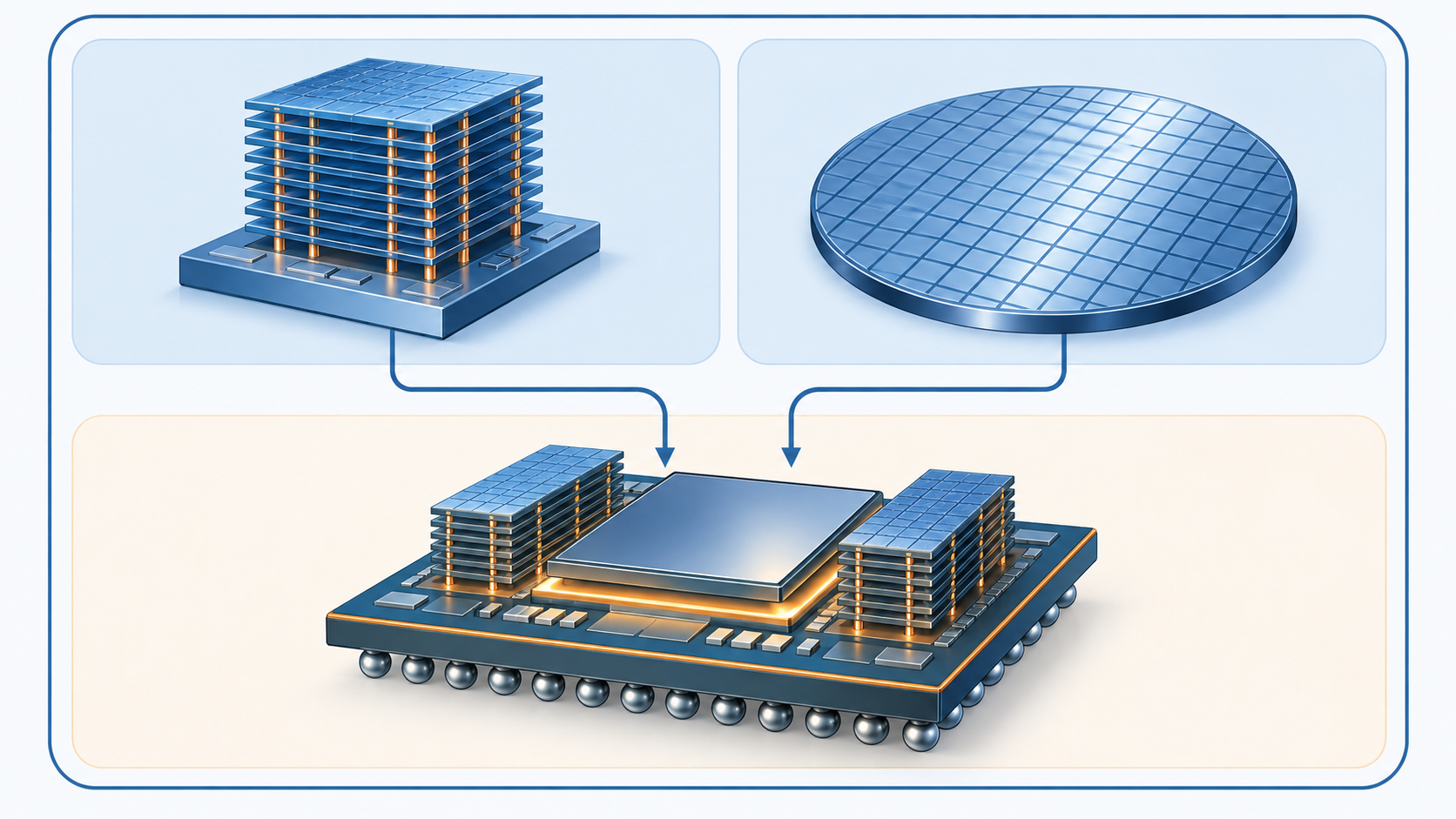
- High bandwidth memory: DRAM stacked vertically to gain bandwidth. It sits next to an AI GPU and is built into the advanced package. For the fourth quarter of 2025 the company said it had grown HBM sales in a supply-constrained market, and it has named volume supply of HBM4 as a priority for 2026.
- HBM base die (4nm)
- The logic die laid under an HBM stack. From the HBM4 generation this became a job for an advanced logic process. The company states in its statutory filing that it has begun volume production of the HBM4 base die on a 4nm process.
- Processes built for 2.5D and 3D packaging
- Of the fourth-generation 4nm process that entered volume production in November 2024, the company writes that it supports advanced 2.5D and 3D packaging. The front-end process, in other words, is designed around the packaging scheme that will follow it.
Put those three side by side and the intent becomes legible. Build the HBM, build the base die under it in your own foundry, and own the advanced package that carries both. The single line the company set out as its direction for 2026, offering an optimised combination of logic, memory and advanced packaging, is exactly that construction Sourced.
On market share, plainly
Samsung Electronics discloses neither its back-end revenue nor its HBM capacity. Figures of the form "HBM world share is X per cent" or "packaging capacity is Y wafers a month" are estimates from research firms or the press, not primary material, and this article does not use them Not yet confirmed.
The statutory filing does carry a DRAM market share figure, but its own footnote states that the data comes from the research firm DRAMeXchange. Appearing in a statutory document does not make an outside estimate a primary source, so this article does not use that number either Not yet confirmed.
Only three things can be stated with confidence from primary sources.
- Non-memory revenue, which contains the back end, was at most KRW 26.0tn in 2025 (section 5 and Fig. 2) Our calculation
- Volume production of the HBM4 base die has begun on a 4nm process, which is primary evidence that the company sits at the junction of advanced logic and advanced packaging Sourced
- The company has written into its 2026 direction that it will offer logic, memory and advanced packaging together Sourced
There is one useful indirect indicator: the weight of the DS Division within the group as a whole. HBM, base dies and advanced packaging all live inside that division.
The tilt has grown sharper since
The 2026 figures make that imbalance far more pronounced Sourced.
| Measure | Full year 2025 | Second quarter 2026 |
|---|---|---|
| Group revenue | KRW 333.6tn | KRW 171.5tn |
| Group operating profit | KRW 43.6tn | KRW 89.5tn |
| DS Division revenue | KRW 130.1tn | KRW 127.5tn |
| DS Division operating profit | KRW 24.9tn | KRW 89.2tn |
A single quarter of 2026 produced more than twice the operating profit of the whole of 2025, at a DS Division operating margin of 70%. The company attributes this to moving ahead of AI server demand and to record bit shipments in both DRAM and NAND. First-half 2026 revenue was KRW 305.4tn, up 98.7% on the same period a year earlier.
8. Current investment plans
According to the U.S. Department of Commerce and NIST, the direct funding of up to US$4.745bn covers two advanced logic fabs for 2nm at Taylor, Texas, one R&D fab at the same site, and an FD-SOI expansion at the existing Austin plant. The company is reported in the same material as planning to invest more than US$37bn in the region Sourced.
No advanced packaging plant appears in that list. The contrast with TSMC, which names two advanced packaging facilities in its own U.S. investment breakdown, is direct: the Samsung Electronics plan for the United States leans towards the front end. Note also that Samsung Electronics publishes no numerical capital budget for the year ahead. Where TSMC gives a range, US$52bn to US$56bn for 2026, Samsung does not, so full-year 2026 investment is undetermined as this article is written Not yet confirmed.
9. Major corporate partners
The counterparties named in the Samsung Electronics statutory disclosure fall into three quite different kinds, which are easily conflated, so they are separated here.
| Kind | Counterparty | Substance | Primary source |
|---|---|---|---|
| Long-term supply contract | Tesla, Inc. | Contract manufacturing of semiconductors by the Foundry business. Signed 26 July 2025, running from July 2025 to December 2033. Contract value US$16,544m | 2025 Business Report Sourced |
| Major customers | Alphabet, Apple, Deutsche Telekom, Hong Kong Techtronics, Supreme Electronics | The five 2025 customers the company lists in alphabetical order. Together they account for about 15% of revenue. Individual amounts are not disclosed | 2025 Business Report Sourced |
| Patent cross-licences | Google (January 2014), Ericsson (May 2021), Qualcomm (July 2022), Huawei (July 2022), Nokia (January 2023) | Agreements giving each side access to the other's patents, preserving freedom to operate. The financial terms are withheld as trade secrets | 2025 Business Report Sourced |
| Software licence | A licence to carry Google applications, the Play store, YouTube and others, across 32 countries of the European Economic Area. 27 February 2019 to 31 March 2026 | 2025 Business Report Sourced | |
| Government | U.S. Department of Commerce (NIST) | Counterparty to the CHIPS Act funding described in section 8 | NIST published material Sourced |
On the Tesla contract value: in the statutory filing, the table in Chapter XI, "Other information", gives 16,544 under a heading of "USD mil", while the long-term contract table in Chapter II places the same 16,544 under a heading of "KRW 100 mil". The unit labels in the English translation contradict each other, and this article follows Chapter XI, which states the figure in U.S. dollars Not yet confirmed.
Which AI chipmakers receive Samsung HBM, and whose films and resins are used in the stacking and packaging, are questions the Samsung Electronics statutory disclosure does not answer at all. The only customers the company names are the five listed alphabetically, plus Tesla. These trading relationships are discussed in counterparties' own disclosure and in trade coverage, but they cannot be confirmed from Samsung's primary material, so this article does not treat them as partnerships Not yet confirmed.
10. Where the company is heading in this field
Anything said here is a forecast, so the established facts and the outlook drawn from them are kept apart.
What is established
| Fact | What it implies for the back end |
|---|---|
| Volume production of the HBM4 base die has begun on a 4nm process | The die underneath an HBM stack became advanced logic work, joining the memory business to the foundry business inside the back end |
| The 2026 direction explicitly promises logic, memory and advanced packaging offered together | The company itself has placed integrated supply, back end included, at the centre of how it intends to compete |
| In the second quarter of 2026 the DS Division earned KRW 89.2tn of operating profit, a 70% margin | Investment capacity has grown abruptly. The means to step up capital spending are there |
| First-generation 2nm is in volume production and the second generation is due in the second half of 2026 | Plans are built on continuing to hold leading-edge logic in house |
| A contract manufacturing agreement with Tesla worth US$16.5bn runs to 2033 | A customer has been secured who underpins foundry utilisation over the long term |
| U.S. CHIPS support covers only front-end fabs and an R&D fab | A U.S. back-end presence is, at the very least, outside the subsidy framework |
| The company writes that roughly five firms capable of very large capital spending dominate the foundry market | Its own view is that the number of players who could attempt integrated supply is structurally small |
Outlook
Not yet confirmed Read plainly, those facts point to Samsung Electronics' presence in the back end growing not as a company that assembles packages, but as the company that can ship HBM and its base die together. On the packaging step itself, on anything resembling CoWoS, it has not matched TSMC. But the number of firms able to supply both the contents of the package and the die underneath them is very small indeed.
Not yet confirmed Two developments could change that picture. One is Samsung Electronics actually making integrated supply of logic, memory and packaging work, at which point a genuine counterweight to the single-supplier structure around TSMC would exist for the first time. The other is the opposite: its position as an HBM supplier weakening. Neither has resolved as of September 2026, and no plan for a back-end site in the United States has been published, so anyone selling materials or equipment would be wise, for now, to plan around the Korean sites.
11. The risks this company carries
What follows is narrowed to the figures in the statutory filings that matter in a back-end context Sourced.
| Risk | Substance | Supporting figures |
|---|---|---|
| The swing of the memory cycle | Revenue moves little while profit moves enormously. Operating profit fell to KRW 6.57tn in 2023 | KRW 43.38tn in 2022 against KRW 6.57tn in 2023, a fall of 84.9% Our calculation |
| Profitability of the foundry business | For the fourth quarter of 2025 the company states that revenue rose on U.S. and Chinese demand, but that provisions limited the improvement in earnings | As written in the fourth-quarter 2025 earnings presentation |
| The weight of capital spending | Capex of KRW 52.65tn in 2025 was 15.8% of revenue, and nine tenths of it went to the DS Division | Capex divided by revenue equals 15.8%; the DS share is 90.2% Our calculation |
| Dependence on a single contract | On the Tesla agreement the company itself notes that the term and the value may change with customer demand and business conditions | A note to Chapter XI of the 2025 Business Report |
| The weight of the Chinese sites | Among the semiconductor manufacturing subsidiaries, Xi'an (SCS) recorded KRW 8.64tn of revenue in 2025. By region, revenue from China was KRW 47.31tn | Summary financial data for major consolidated subsidiaries, and revenue by region |
| Conditions on the subsidies | KRW 1.72tn of government grants was received in 2025, but neither the breakdown nor the conditions are disclosed | Consolidated cash flow statement; nothing was recorded in 2024 |
Say "back-end materials" and the first things named are interposer substrates, underfill, mould compound and ABF, Ajinomoto Build-up Film. Those belong to the package assembly layer, of the sort CoWoS uses, and the choice among them is made by whoever assembles the package.
With Samsung Electronics, the back-end activity is mainly inside the HBM stack: the layer where DRAM dies are piled up and bonded to one another. What is wanted there is die-attach material and interlayer bonding material, a different family altogether from package assembly. The same phrase, back-end materials, describes completely different property requirements depending on which customer you are facing.
That said, which bonding method and which material system Samsung uses in HBM stacking is absent from the statutory filings and could not be confirmed for this article Not yet confirmed. From the materials side, the fact that the chosen method is never published is itself what makes this customer awkward to plan around.
12. Glossary
- IDM
- Integrated Device Manufacturer. A chipmaker that carries design, manufacturing, assembly and test in house. Samsung Electronics, Intel and Micron are examples.
- Foundry
- The business of building semiconductors other companies have designed. Samsung Electronics is an IDM that also runs a foundry, so it competes with TSMC while selling products of its own.
- HBM
- High Bandwidth Memory. DRAM stacked vertically to gain bandwidth, placed beside an AI GPU and built into the advanced package.
- Base die
- The logic die laid at the bottom of an HBM stack, handling signalling between the stacked DRAM and the outside world. From the HBM4 generation it is built on an advanced logic process.
- 2.5D and 3D packaging
- Placing several dies side by side and linking them through an intermediate substrate (2.5D), or stacking them vertically (3D). Both make up for performance that shrinking a single die can no longer deliver.
- DS and DX Divisions
- The two operating divisions of Samsung Electronics. DS is Device Solutions, the semiconductor side; DX is Device eXperience, covering smartphones, appliances and other finished products.
- Business Report
- The statutory disclosure a listed Korean company files with the Financial Supervisory Service through its DART system. It corresponds to a U.S. Form 10-K or 20-F.
- GDR
- Global Depositary Receipt, an instrument that lets shares trade outside their home market. Samsung Electronics GDRs trade in London.
 AI-generated concept
13. References
- Samsung Electronics 2025 Business Report (the English edition of the Korean statutory disclosure for the 2025 financial year). Legal name, founding date, head office address, listing venues, revenue by segment, revenue by product, revenue by region, R&D expense, capital expenditure, headcount, the list of sites, summary financial data for major consolidated subsidiaries, the definition of production capacity, major customers, long-term contracts, patent cross-licences, the footnote on the source of the DRAM share figure, and the start of HBM4 base die volume production. https://images.samsung.com/is/content/samsung/assets/global/ir/docs/2025_4Q_Interim_Report.pdf
- Samsung Electronics Earnings Presentation: 4Q 2025 Financial Results. Revenue, operating profit and operating margin for 2024 and 2025, segment results, cash flow, the state of the Foundry business and the direction set for 2026. https://images.samsung.com/is/content/samsung/assets/global/ir/docs/2025_4Q_conference_eng.pdf
- Samsung Electronics Earnings Presentation: 4Q 2022 Financial Results. Revenue, operating profit and operating margin for 2021 and 2022. https://images.samsung.com/is/content/samsung/assets/global/ir/docs/2022_4Q_conference_eng.pdf
- Samsung Electronics Earnings Presentation: 4Q 2023 Financial Results. Revenue, operating profit and operating margin for 2023. https://images.samsung.com/is/content/samsung/assets/global/ir/docs/2023_4Q_conference_eng_01.pdf
- Samsung Electronics Earnings Presentation: 2Q 2026 Financial Results. Second-quarter 2026 revenue of KRW 171.5tn and operating profit of KRW 89.5tn, DS Division results, and the plan to expand base die sales in the Foundry business. https://images.samsung.com/is/content/samsung/assets/global/ir/docs/2026_2Q_conference_eng.pdf
- Samsung Electronics 2026 Half-Year Business Report (the English edition of the statutory disclosure for the first half of 2026). First-half 2026 revenue of KRW 305.4tn, first-half capital expenditure of KRW 27.99tn, the company's description of the foundry market, and the footnote on the source of the DRAM share figure. https://images.samsung.com/is/content/samsung/assets/global/ir/docs/2026_Half_Interim_Report.pdf
- Samsung Electronics 2024 Business Report (the English edition of the statutory disclosure for the 2024 financial year). Capital expenditure of KRW 53.65tn in 2024 and its split by division. https://images.samsung.com/is/content/samsung/assets/global/ir/docs/2024_4Q_Interim_Report.pdf
- U.S. NIST (Department of Commerce) CHIPS for America, Samsung Electronics (Texas) award summary. Direct funding of up to US$4.745bn, two advanced logic fabs and one R&D fab at Taylor, the Austin expansion, and the company's regional investment of more than US$37bn. https://www.nist.gov/chips/samsung-electronics-texas-taylor
- Samsung Electronics Official investor relations site, used to check the corporate profile and locate the disclosure documents. https://www.samsung.com/global/ir/
14. Claim-to-source audit
| Claim in the article | Category | Source |
|---|---|---|
| Legal name, founding date (13 January 1969), head office address, listings (Korea Exchange 11 June 1975, London GDR) | Sourced | Reference 1 https://images.samsung.com/is/content/samsung/assets/global/ir/docs/2025_4Q_Interim_Report.pdf |
| 2025 revenue of KRW 333.6tn, operating profit of KRW 43.6tn, up 10.9% year on year | Sourced | References 1 and 2 https://images.samsung.com/is/content/samsung/assets/global/ir/docs/2025_4Q_conference_eng.pdf |
| Revenue for 2021 and 2022 (KRW 279.60tn and 302.23tn) and operating profit (KRW 51.63tn and 43.38tn) | Sourced | Reference 3 https://images.samsung.com/is/content/samsung/assets/global/ir/docs/2022_4Q_conference_eng.pdf |
| 2023 revenue of KRW 258.94tn and operating profit of KRW 6.57tn | Sourced | Reference 4 https://images.samsung.com/is/content/samsung/assets/global/ir/docs/2023_4Q_conference_eng_01.pdf |
| Revenue by segment (DX 56.3%, DS 39.0%, Samsung Display 8.9%, Harman 4.7%, eliminations -8.9%) | Sourced | Reference 1 https://images.samsung.com/is/content/samsung/assets/global/ir/docs/2025_4Q_Interim_Report.pdf |
| Memory revenue of KRW 104.1tn and non-memory of KRW 26.0tn, 80.0% and 20.0% of the DS Division | Our calculation | The difference between DS Division revenue and product revenue in reference 1 https://images.samsung.com/is/content/samsung/assets/global/ir/docs/2025_4Q_Interim_Report.pdf |
| DS Division operating profit of KRW 24.9tn, or 57% of the group | Our calculation | Derived from the segment operating profit in reference 1 https://images.samsung.com/is/content/samsung/assets/global/ir/docs/2025_4Q_Interim_Report.pdf |
| 128,881 employees, with the splits by division and by sex and the average tenure (Korea-only parent basis) | Sourced | Reference 1 https://images.samsung.com/is/content/samsung/assets/global/ir/docs/2025_4Q_Interim_Report.pdf |
| The DS Division as 60.6% of the Korean workforce (78,064 people) | Our calculation | The male and female figures in the headcount table of reference 1, added together https://images.samsung.com/is/content/samsung/assets/global/ir/docs/2025_4Q_Interim_Report.pdf |
| R&D expense (KRW 28.35tn in 2023, 35.02tn in 2024, 37.75tn in 2025) and the share of revenue | Sourced | Reference 1 https://images.samsung.com/is/content/samsung/assets/global/ir/docs/2025_4Q_Interim_Report.pdf |
| 2024 capital expenditure of KRW 53.65tn, of which KRW 46.28tn in the DS Division | Sourced | Reference 7 https://images.samsung.com/is/content/samsung/assets/global/ir/docs/2024_4Q_Interim_Report.pdf |
| First-half 2026 revenue of KRW 305.4tn and capital expenditure of KRW 27.99tn | Sourced | Reference 6 https://images.samsung.com/is/content/samsung/assets/global/ir/docs/2026_Half_Interim_Report.pdf |
| Second-quarter 2026 revenue of KRW 171.5tn and operating profit of KRW 89.5tn, with the DS Division at KRW 127.5tn and 89.2tn | Sourced | Reference 5 https://images.samsung.com/is/content/samsung/assets/global/ir/docs/2026_2Q_conference_eng.pdf |
| Memory capacity defined as converted shipment volume after packaging divided by utilisation, and 2025 memory output | Sourced | Reference 1 https://images.samsung.com/is/content/samsung/assets/global/ir/docs/2025_4Q_Interim_Report.pdf |
| Volume production of the HBM4 base die on 4nm, and fourth-generation 4nm supporting 2.5D and 3D packaging | Sourced | Reference 1 https://images.samsung.com/is/content/samsung/assets/global/ir/docs/2025_4Q_Interim_Report.pdf |
| The 2026 direction on integrated logic, memory and advanced packaging, and the start of first-generation 2nm volume production | Sourced | Reference 2 https://images.samsung.com/is/content/samsung/assets/global/ir/docs/2025_4Q_conference_eng.pdf |
| Twelve domestic sites; SAS (Austin) revenue of KRW 3.76tn; SCS (Xi'an) revenue of KRW 8.64tn; SESS (Suzhou) as toll processing | Sourced | Reference 1 https://images.samsung.com/is/content/samsung/assets/global/ir/docs/2025_4Q_Interim_Report.pdf |
| The Tesla contract (26 July 2025, running to December 2033, US$16,544m) and five major customers at about 15% of revenue | Sourced | Reference 1 https://images.samsung.com/is/content/samsung/assets/global/ir/docs/2025_4Q_Interim_Report.pdf |
| U.S. CHIPS Act direct funding of up to US$4.745bn, covering two advanced logic fabs and an R&D fab at Taylor and the Austin expansion | Sourced | Reference 8 https://www.nist.gov/chips/samsung-electronics-texas-taylor |
| KRW 1.72tn of government grants received in 2025, with nothing recorded in 2024 | Sourced | Reference 1 https://images.samsung.com/is/content/samsung/assets/global/ir/docs/2025_4Q_Interim_Report.pdf |
| Capex at 15.8% of revenue, the DS share at 90.2%, and the 84.9% fall in operating profit in 2023 | Our calculation | Derived from the figures in references 1 and 4 https://images.samsung.com/is/content/samsung/assets/global/ir/docs/2025_4Q_Interim_Report.pdf |
| Samsung Electronics back-end revenue, meaning packaging and test, on its own | Not yet confirmed | Not disclosed. Our calculation gives only the ceiling of KRW 26.0tn |
| HBM world share and packaging capacity | Not yet confirmed | No primary source exists, so this article states no figure |
| DRAM market share | Not yet confirmed | It appears in the statutory filing, but a footnote attributes it to the research firm DRAMeXchange, so this article does not use it |
| Which of the twelve domestic sites handle back-end assembly and test | Not yet confirmed | Absent from the statutory filings, and this article does not fill the gap by inference |
| The full-year 2026 capital expenditure plan | Not yet confirmed | The company publishes no numerical budget for the coming year, so this article gives actuals only |
| The currency unit of the Tesla contract value | Not yet confirmed | Two headings within the same filing, "USD mil" and "KRW 100 mil", contradict each other; this article follows Chapter XI, which states dollars |
| Bonding methods and material systems used in HBM stacking, HBM customers, and dealings with back-end materials makers | Not yet confirmed | Absent from the statutory filings, so this article does not treat them as partnerships |
| The outlook in section 10 | Not yet confirmed | An interpretation by this article, drawn from the seven items in the facts table |
Last updated 21 September 2026 / Troy Technical
Every figure in this article comes from the business reports Samsung Electronics publishes under the Korean statutory
disclosure regime, from the company's own earnings presentations, and from material published by NIST at the U.S.
Department of Commerce. No research-firm estimates or press-based figures have been used. Won amounts are given in won,
because the company publishes no U.S. dollar translation of them.