TECHNOLOGY EXPLAINER
Optical Connectors and Fiber Attach
— one micrometer of misalignment decides the loss
To "connect" light is to bring two light paths about 10 µm across face to face with better than 1 µm accuracy. What delivers that accuracy is a molded plastic part, a V-groove in glass, and an adhesive. Fujikura has reported a connector whose plastic ferrule holds core offset to 0.23 µm on average, and IBM researchers have discussed how to bridge the gap between the ±10 µm placement accuracy of chip-assembly tools and the 1 to 2 µm that single-mode optics needs.
- What optical connectors and fiber attach are (the short version)
- What is lost at a joint: four causes, plus reflection
- Our calculation: how many dB a 1 µm lateral offset costs
- Joining one fiber: ferrules and split sleeves
- Joining many at once: MT and MPO
- A materials engineer's view (1): the precision comes from a molded plastic part
- Joining fiber to chip: arrays, self-alignment and 3D printing
- A materials engineer's view (2): one adhesive is not enough
- Open problems and unconfirmed points
- Glossary / References / Claim-to-source audit
Sourced = stated in a learned-society reference, a paper or a company's published material (link given)
Our calculation = a figure this article derived from assumptions it spells out
Not yet confirmed = a plan or target with no confirmed track record yet
Structural readings and materials-design interpretations are marked separately as commentary.
Company figures are labelled as guaranteed product values, measurements on samples, or measurements from research reports, as the case may be.
1. What optical connectors and fiber attach are (the short version)
An optical connector is a component that positions the cores of two optical fibers precisely and removes the gap between them so that light can pass across. The IEICE Knowledge Base, a reference work published by Japan's Institute of Electronics, Information and Communication Engineers, says that what matters in joining optical fibers is whether the cores of the two fibers can be positioned precisely and the gap between them eliminatedSourced.
- Two kinds of joint: permanent joints such as fusion splices, made by melting the glass, and connector joints, which can be mated and unmated any number of timesSourced
- What makes it hard: the light path in single-mode fiber is about 10 µm across. Once single-mode fiber became mainstream in the 1980s, joining became harder and more precise components became indispensableSourced
- Where the contest is now: not just fiber to fiber, but attaching fiber to photonic chips. Here adhesives, V-grooves and self-aligning structures take the leading roles (our commentary)
The structure, loss and manufacture of the fiber itself are covered in our optical fiber explainer; couplers on the silicon chip side (edge coupling and vertical coupling) and TSMC's coupling-loss figures in our silicon photonics explainer; and configurations that put optical engines inside the switch package, along with fiber-array adhesives shown at trade fairs, in our explainer on co-packaged optics. This article narrows the focus to how the parts are aligned and what holds them in place (our own division of topics).
2. What is lost at a joint: four causes, plus reflection
The Knowledge Base divides the causes of splice loss in single-mode fiber into four and gives a formula for eachSourced: a gap between the end faces, angular misalignment, lateral (axial) offset and mode field diameter mismatch.
Alongside loss, reflection matters. At a boundary between materials of different refractive index, part of the light bounces back (Fresnel reflection). Taking the core index as 1.454, the Knowledge Base states that when a fiber end face meets air, 3.4% of the incident light returns (a return loss of 14.7 dB), and it calls this a value too large to ignore for transmission performanceSourced. That is why a connector either presses the end faces into physical contact (PC connection) or fills the gap with a material of similar index (index-matching material).
3. Our calculation: how many dB a 1 µm lateral offset costs
The Knowledge Base gives the fraction of light that passes (the transmission coefficient) T when the centers of two fibers are offset sideways by d, using the mode field radius ω, as T = exp{−(d/ω)²}Sourced. Here is what happens when numbers are put into it.
- Assumption 1 (standard single-mode fiber): mode field diameter 9.2 µm (the top of G.652.D's range of nominal values) → radius ω = 4.6 µm
- Assumption 2 (a small light path): a mode on the photonic-chip side, assumed to be 3 µm across (ω = 1.5 µm)
- Converted to loss as loss (dB) = −10 log TOur calculation
| Lateral offset d | ω = 4.6 µm (standard fiber) | ω = 1.5 µm (assumed small mode) |
|---|---|---|
| 0.5 µm | about 0.05 dB | about 0.48 dB |
| 1.0 µm | about 0.21 dB | about 1.9 dB |
| 1.3 µm | about 0.35 dB | about 3.3 dB |
| 2.0 µm | about 0.82 dB | about 7.7 dB |
Assumptions and limits: the formula approximates the light distribution as Gaussian and excludes end-face gaps, angular misalignment and reflection. ω = 1.5 µm is an assumption made in this article; real on-chip couplers are designed to expand the mode, and the values change greatly with the design.
The same 1 µm offset costs 0.2 dB if the light path is wide and about 2 dB if it is narrowOur calculation. That is why widening the light before joining it is the basic principle of fiber attach (our commentary). The paper by IBM researchers discussed in Section 7 likewise says that the aligned connections are made at the point of maximum mode delocalization, where the mode is most spread outSourced.
4. Joining one fiber: ferrules and split sleeves
The Knowledge Base describes optical connectors developed and commercialized in Japan. According to it, almost all single-fiber, single-mode connectors of the PC type consist of two cylindrical precision ferrules and one cylindrical split sleeveSourced.
| Connector | What the Knowledge Base says |
|---|---|
| FC (1979) | The first single-fiber connector in practical use, and the first to adopt a precision ferrule and split sleeve, with a threaded coupling. Improved dimensional accuracy of the fiber made a simple structure without core alignment possible |
| SC | Adopted a zirconia ferrule, changed the plug from round metal to square plastic and the coupling from threaded to push-pull, lowering cost and making mating and unmating easy |
| MU | Slimmed the ferrule diameter from 2.5 mm to 1.25 mm, greatly improving packing density |
| PC / APC | PC connection, which brings end faces into physical contact, and angle-polished APC, which suppresses reflection greatly, were developed, achieving lower loss and lower reflection |
All Sourced (IEICE Knowledge Base, Group 5, Part 2, Chapter 5 [Ref. 1]).
One sentence in the Knowledge Base should not be missed. It says that tightening the fiber outer-diameter specification from an early 125 ±3 µm to 125 ±1 µm is what made it possible to reduce connector lossSourced. A connector's performance is not decided by the connector alone. The dimensional accuracy of the glass it holds is what allowed the connector design to become simple (our commentary).
5. Joining many at once: MT and MPO
In data centers and optical engines, dozens of fibers are connected at once. The multi-fiber connectors that do this are MT and MPO.
| Item | MT | MPO |
|---|---|---|
| Development | 1980s. Developed with high-precision plastic molding to join ribbon fibers (4 to 16 fibers) in one go | Around 1990. Uses MT ferrules, with push-pull mass connection |
| Alignment | Two guide pins inserted into guide holes | Same (MT ferrule built in) |
| Retention | Clamped with a clamp spring | Push-pull operation through an adapter |
| Handling the gap between end faces | Index-matching material used to suppress Fresnel reflection | Fibers polished from an angled end face protrude slightly, giving a PC connection without matching material |
All Sourced (IEICE Knowledge Base, Group 5, Part 2, Chapter 5 [Ref. 1]).
In a 2020 issue of its technical review, Fujikura reported evaluation results for a low-loss single-mode MPO connector (ULL MPO)Sourced.
| Item | 12-fiber ULL MPO | 24-fiber ULL MPO |
|---|---|---|
| Interface standard | IEC 61754-7-1 ed.1 | IEC 61754-7-2 ed.1 |
| Fiber core offset | 0.23 µm average, 0.46 µm max. | 0.27 µm average, 0.49 µm max. |
| Insertion loss (1.31 µm, no matching agent, random mating) | 0.05 dB average, 0.17 dB max. | 0.05 dB average, 0.18 dB max. |
| Max. insertion loss over 50 mating cycles | 0.15 dB or less | 0.20 dB or less |
| Return loss | 64.7 dB average, 60.2 dB min. | 63.7 dB average, 55.7 dB min. |
All Sourced (Fujikura Technical Review No. 133, 2020 [Ref. 2]). The same report puts the achievable performance of earlier low-loss MPO connectors at about 0.25 dB maximum. These are measurements from a research report, not guaranteed product values.
6. A materials engineer's view (1): the precision comes from a molded plastic part
Fujikura's report states that the insertion loss of an MPO connector depends heavily on the core offset of the fibers mounted in the MT ferrule, and explains that core offset depends on the position of the fiber holes, the clearance between the cladding diameter and the hole, and the concentricity of core and claddingSourced. The MT ferrule is made of PPS (polyphenylene sulfide) resin, and the report attributes the average core offset of 0.23 µm to high-precision molding technology for the MT ferruleSourced.
Put into the calculation in Section 3, a 0.23 µm offset costs standard fiber only about 0.01 dBOur calculation (from exp{−(0.23/4.6)²}). In other words, a molded plastic part is delivering accuracy good enough for an optical component.
Three materials issues overlap here (our commentary).
- Molding shrinkage: resin shrinks as it cools in the mold. Aiming hole positions at sub-micrometer accuracy calls for mold design and material choice that allow for the amount and spread of shrinkage
- Fillers and thermal expansion: when the temperature changes, so does the hole spacing. If this differs greatly from the thermal expansion of the silica glass it holds, it shows up as offset
- Bond-line thickness: fibers are bonded into the holes. That "clearance" is listed as a loss factor means the adhesive layer of a few micrometers or less between hole and fiber is part of the precision budget too
As Section 4 showed, single-fiber connectors also reached low loss because the fiber diameter specification was tightened from ±3 µm to ±1 µmSourced. The precision of an optical joint is set by the stack-up of dimensional tolerances in glass, resin and adhesive (our commentary).
7. Joining fiber to chip: arrays, self-alignment and 3D printing
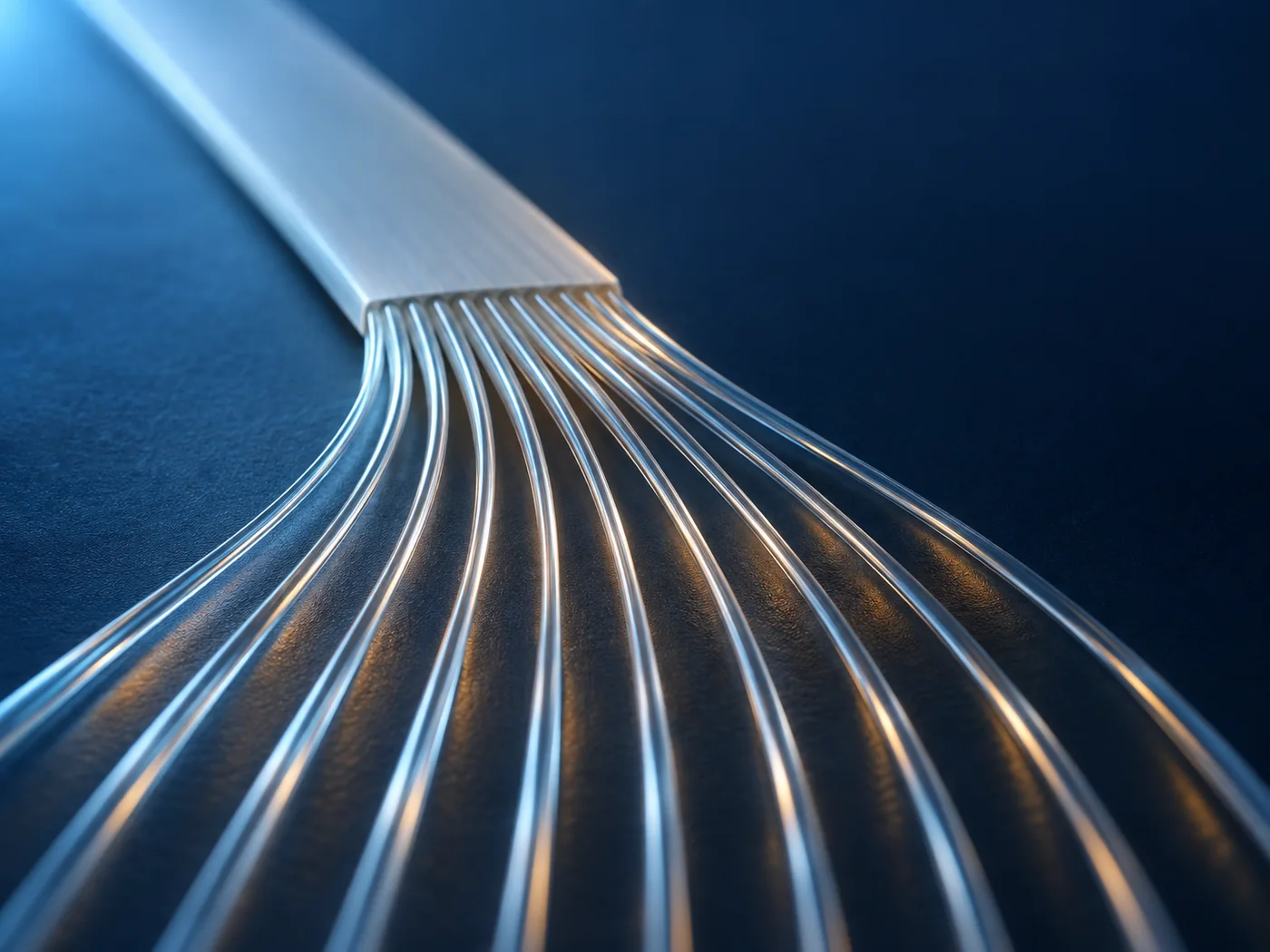
The technology for joining fiber to fiber has been refined over decades. What is hard now is joining fiber to a photonic chip. In a 2016 paper, IBM researchers framed the problem as followsSourced.
The placement uncertainty of high-throughput pick-and-place tools can be as large as ±10 µm. That is highly inadequate for single-mode photonics, where even the large mode of a standard cleaved fiber needs alignment to at least 1 to 2 µm for acceptable coupling efficiencySourced.
The gap is bridged by mode engineering and self-alignmentSourced.
Self-alignment in V-grooves: from chip-level to wafer-level
The core of the approach by Barwicz and colleagues is building the alignment accuracy into the wafer process. If V-grooves are made on the chip by lithography and etching and the fiber is dropped into them, its position is fixed even if placement is coarse. In an analysis combining 10,000 random variations in fiber diameter, core concentricity and ellipticity with variations in V-groove lithography, hardmask opening and anisotropic etching, the paper finds that the residual misalignment is below ±1.3 µm at 3σSourced.
A 2018 paper by the same group describes this idea as moving complexity from chip-level assembly to wafer-level planar processing, and reports peak transmission of −1.3 dB from standard fiber to chip and −1.1 dB from chip to chipSourced. In the table in Section 3, ±1.3 µm cost standard fiber about 0.35 dBOur calculation. The numbers show why V-grooves pair only with the large mode of standard fiber. The paper itself notes that with small-mode fiber, this level of misalignment could bring a significant coupling penaltySourced.
Printing optics onto the facet
The other direction is to match the shape of the light itself. In 2018, Dietrich and colleagues at Karlsruhe Institute of Technology (KIT) reported in situ 3D nanoprinting of free-form beam-shaping elements directly on the facets of chips and fibers. They say the approach matches very different mode shapes while greatly relaxing alignment tolerances, allowing passive assembly, and they demonstrated coupling efficiency of up to 88% between an InP laser and an optical fiberSourced. In 2012, Koos and colleagues (Koos is the senior author of both papers) also published the concept of photonic wire bonding, which links chips with three-dimensional polymer waveguidesSourced.
8. A materials engineer's view (2): one adhesive is not enough
The adhesive between a fiber array and a chip is a material the light passes through. NTT-AT lists the following features for its adhesives for optical path couplingSourced.
- The refractive index can be controlled within 1.456 to 1.567, to an accuracy of ±0.005 (589 nm)
- Compatible with solder reflow (260 °C); high moisture resistance
- Example uses: bonding PLCs to fiber and connecting silicon photonic waveguides to fiber arrays
- Grades include epoxies index-matched to silica glass at 1.55 µm (GA700H with a Tg of 145 °C, GA700L with 46 °C) and acrylates that meet Telcordia high-temperature, high-humidity requirements
The reason for matching the index to ±0.005 is the Fresnel reflection of Section 2. The smaller the index difference at an interface, the smaller the reflection. The index of the adhesive is a variable in the optical design (our commentary).
Look inside a fiber array, though, and the adhesive is not in one place only. NTT-AT offers separate adhesives for fiber-array assembly: for fixing in V-grooves (low viscosity) and for fixing the fiber at its root (non-flowing paste)Sourced.
| Use | Example grade | Base resin | Tg | Features (as stated by the company) |
|---|---|---|---|---|
| V-groove fixing | AT9390 | Epoxy | 131 °C | Viscosity 600 mPa·s, high moisture resistance |
| V-groove fixing | AT3925M | Epoxy | 219 °C | Viscosity 200 mPa·s, high modulus, high heat resistance |
| Root fixing | AT9575M | Epoxy | 42 °C | Paste; high durability, non-flowing, transparent |
| Root fixing | AT8105 | Acrylate | 103 °C | Paste; high durability, non-flowing, high Tg |
All Sourced (NTT-AT product information [Refs. 7 and 8]). The company describes the values in the table as measurements on samples, not guaranteed values. All are UV-curing.
At ECTC 2018, IBM researchers presented a paper whose title states this idea outright: "Solder-Reflowable, High-Throughput Fiber Assembly Achieved by Partitioning of Adhesive Functions". By partitioning the functions of the adhesive, they combined resistance to solder reflow up to 260 °C, almost no increase in optical loss at operating temperatures up to 150 °C, and a short tacking time suited to high-speed assembly toolsSourced.
Asking one adhesive to be transparent, index-matched, low in viscosity so it flows into gaps, fast-curing, reflow-proof, moisture-resistant and stress-relieving all at once is asking too much. Optical properties where the light passes; strength and heat resistance where the parts are held mechanically; non-flow and flexibility at the fiber root. NTT-AT's split of grades and the title of the IBM paper read as the same conclusion reached from different positions (our commentary).
The group's 2016 paper goes further and treats the thickness of the adhesive itself as a design value. It says the adhesive layer between the polymer waveguide and the silicon should preferably be no more than 1 µm through the section where light is handed over, and that near the chip edge a thicker layer is instead desirable to prevent scatteringSourced. It also says that the area where the silicon substrate is undercut to let the mode expand is filled with a low-index adhesive at assemblySourced. The adhesive is acting as the optical cladding, the layer that confines the light (our commentary).
9. Open problems and unconfirmed points
(1) The more fibers, the more the spread matters
Dozens of fibers connect to an optical engine (see our silicon photonics explainer). Even if the maximum insertion loss of an MPO is about 0.25 dB per joint (the achievable performance Fujikura gives for earlier low-loss MPO connectors), four of them along a link add up to as much as 1 dBOur calculation (0.25 × 4, a simple worst-case sum). Each increase in fiber count raises the question of how tightly the spread of maximum values, not the average, can be held (our commentary).
(2) Reconciling small modes with passive assembly
As the calculation in Section 3 shows, the smaller the mode, the less tolerant it is of misalignmentOur calculation. Approaches that expand the mode with mode converters or 3D-printed lenses have been proposedSourced, but which approach will become the standard for volume production had not been settled at the time of writingNot yet confirmed.
(3) Standards for pluggable connections at the chip
Fiber-to-fiber MPO connectors conform to IEC interface standardsSourced. By contrast, no widely adopted common standard for a pluggable connection between chip and fiber could be confirmed within the scope of this articleNot yet confirmed.
(4) Long-term reliability data for adhesives
NTT-AT's values are measurements on samples, and the company says they are not guaranteedSourced. This article has not confirmed quantitative values from primary sources for long-term index drift or degradation of the bonded interface under high temperature and humidity.
- Splice loss has four causes: gap, angular tilt, lateral offset and MFD mismatch. An air gap reflects about 3.4% at each end faceSourced
- A 1 µm lateral offset costs standard fiber about 0.2 dB and a narrow mode about 2 dBOur calculation
- Sub-micrometer positions are set by a molded PPS part. Fujikura reports an average core offset of 0.23 µmSourced
- Chip attach is about bridging the gap between ±10 µm placement accuracy and the 1 to 2 µm required. V-groove self-alignment and 3D printing on facets have been reportedSourced
- Adhesives are optical materials, with a different role in each place. Index control to ±0.005 and 260 °C reflow resistance through partitioned functions have been shownSourced
10. Glossary
- Insertion loss
- The amount of light lost in passing through a joint, in dB.
- Return loss
- How little light comes back from a joint, in dB. The larger the value, the less the reflection.
- Fresnel reflection
- Reflection of part of the light at a boundary between materials of different refractive index.
- Lateral offset
- A sideways displacement between the centers of two facing cores.
- Mode field diameter (MFD)
- The diameter over which the light is effectively spread. Used to calculate splice loss.
- Ferrule
- A precision cylinder that holds a fiber in its central hole. Zirconia is typical for single-fiber types.
- Split sleeve
- A tube slit along part of its length. Two ferrules are inserted into it to align their centers.
- PC connection
- Physical Contact. A connection in which the fiber end faces are pressed into physical contact.
- APC
- Angled PC. The end face is polished at an angle so that reflected light is less likely to return into the fiber.
- Index-matching material
- A material that fills the gap between fiber end faces and suppresses reflection caused by the index difference.
- MT / MPO
- Multi-fiber connectors that align many fibers at once with guide pins. MPO is a push-pull type that uses MT ferrules.
- Ribbon fiber
- Several fibers laid flat side by side and held together by a coating.
- Fiber array
- A component in which several fibers are laid and fixed in a V-grooved substrate and the end face is polished.
- V-groove
- A groove with a V-shaped section. Dropping a fiber into it fixes the fiber's position.
- Self-alignment
- An arrangement in which the fit of shapes makes parts settle into position on their own.
- Active alignment
- Passing light through while watching the output, finding the position of best coupling and fixing it there.
- Tg (glass transition temperature)
- The temperature at which a resin changes from a hard glassy state to a soft rubbery one.
- Solder reflow
- The heating step used to solder components to a board. Heat resistance up to about 260 °C is required.
11. References (primary sources)
- IEICE Knowledge Base Group 5, Part 2, Chapter 5 "Optical connection technology" (ver. 3, 4 June 2018, PDF, in Japanese) https://www.ieice-hbkb.org/files/05/05gun_02hen_05.pdf
- Fujikura Shuhei Kanno et al., "Ultra Low Loss (ULL) MPO connector", Fujikura Technical Review No. 133 (2020, PDF, in Japanese) https://www.fujikura.co.jp/research/pdf/technical-report/133/133_R3_1.pdf
- T. Barwicz et al. (IBM) "A Novel Approach to Photonic Packaging Leveraging Existing High-Throughput Microelectronic Facilities", IEEE Journal of Selected Topics in Quantum Electronics 22(6), 8200712 (2016) https://doi.org/10.1109/JSTQE.2016.2593637
- T. Barwicz et al. "Automated, high-throughput photonic packaging", Optical Fiber Technology 44, 24–35 (2018) https://doi.org/10.1016/j.yofte.2018.02.019
- P.-I. Dietrich et al. (KIT) "In situ 3D nanoprinting of free-form coupling elements for hybrid photonic integration", Nature Photonics 12, 241–247 (2018) https://doi.org/10.1038/s41566-018-0133-4
- A. Janta-Polczynski et al. (IBM) "Solder-Reflowable, High-Throughput Fiber Assembly Achieved by Partitioning of Adhesive Functions", 2018 IEEE ECTC, pp. 1109–1117 https://research.ibm.com/publications/solder-reflowable-high-throughput-fiber-assembly-achieved-by-partitioning-of-adhesive-functions
- NTT-AT "Adhesives for optical path coupling", product information https://keytech.ntt-at.com/adhesive/prd_10011.html
- NTT-AT "Adhesives for fiber array assembly", product information https://keytech.ntt-at.com/adhesive/prd_10012.html
- N. Lindenmann et al. (with C. Koos) "Photonic wire bonding: a novel concept for chip-scale interconnects", Optics Express 20, 17667 (2012) https://doi.org/10.1364/OE.20.017667
12. Claim-to-source audit
| Claim in the text | Basis | Label |
|---|---|---|
| That what matters in joining is precise positioning of the cores and elimination of the gap. The two kinds of joint, permanent and connector. That single-mode became mainstream in the 1980s, making greater precision indispensable. The four loss causes and the lateral-offset formula T = exp{−(d/ω)²}. The 3.4% end-face reflectance in air (14.7 dB, n1 = 1.454) and that it is too large to ignore. The development of PC and APC. That tightening the fiber diameter specification from 125 ±3 µm to 125 ±1 µm made lower connector loss possible. The descriptions of FC (1979), SC (zirconia, square plastic, push-pull) and MU (2.5 to 1.25 mm). That PC-type single-fiber connectors consist of two precision ferrules and one split sleeve. MT (1980s, high-precision plastic molding, two guide pins, clamp spring, index-matching material) and MPO (around 1990, angled end face, PC connection without matching material through fiber protrusion) | Reference 1 https://www.ieice-hbkb.org/files/05/05gun_02hen_05.pdf | Sourced |
| That the ULL MPO interfaces conform to IEC 61754-7-1 and 7-2. That the MT ferrule is PPS resin. That insertion loss depends heavily on core offset, which depends on hole position, clearance and concentricity. Core offset (12-fiber 0.23 average / 0.46 µm max.; 24-fiber 0.27 average / 0.49 µm max.), insertion loss (0.05 dB average, 0.17 / 0.18 dB max.), max. 0.15 / 0.20 dB or less over 50 matings, and return loss. That the achievable performance of earlier low-loss MPO is about 0.25 dB max. | Reference 2 https://www.fujikura.co.jp/research/pdf/technical-report/133/133_R3_1.pdf | Sourced |
| That pick-and-place placement accuracy can be ±10 µm and that even standard fiber needs alignment to 1 to 2 µm. That the gap is bridged with mode engineering and self-alignment. That aligned connections are made at maximum mode delocalization. The Monte Carlo analysis of V-groove self-alignment giving below ±1.3 µm at 3σ, and that small-mode fiber could suffer a significant penalty. That the substrate is undercut for mode expansion and filled with low-index adhesive. That the adhesive layer should be no more than 1 µm through the adiabatic crossing and thicker at the chip edge | Reference 3 https://doi.org/10.1109/JSTQE.2016.2593637 | Sourced |
| That complexity moves from chip-level assembly to wafer-level planar processing. Peak transmission of −1.3 dB from standard fiber to chip and −1.1 dB chip to chip | Reference 4 https://doi.org/10.1016/j.yofte.2018.02.019 | Sourced |
| In situ 3D nanoprinting of free-form beam-shaping elements on facets, relaxed alignment tolerances and passive assembly, and coupling efficiency of up to 88% between an InP laser and fiber | Reference 5 https://doi.org/10.1038/s41566-018-0133-4 | Sourced |
| That partitioning adhesive functions achieved reflow resistance up to 260 °C, almost no increase in optical loss at operating temperatures up to 150 °C, and a short tacking time | Reference 6 https://research.ibm.com/publications/solder-reflowable-high-throughput-fiber-assembly-achieved-by-partitioning-of-adhesive-functions | Sourced |
| Index control of the optical path coupling adhesives (1.456 to 1.567, ±0.005, 589 nm), compatibility with 260 °C reflow, high moisture resistance, example uses in PLC/fiber bonding and silicon photonics, GA700H (Tg 145 °C) and GA700L (46 °C) index-matched to silica at 1.55 µm, acrylates meeting Telcordia requirements. That the values are measurements on samples | Reference 7 https://keytech.ntt-at.com/adhesive/prd_10011.html | Sourced |
| That fiber-array assembly adhesives are divided into V-groove fixing (low viscosity) and root fixing (non-flowing). The base resin, Tg, viscosity and features of AT9390, AT3925M, AT9575M and AT8105. UV curing. That the values are sample measurements, not guaranteed values | Reference 8 https://keytech.ntt-at.com/adhesive/prd_10012.html | Sourced |
| That the concept of photonic wire bonding was published in 2012 | Reference 9 https://doi.org/10.1364/OE.20.017667 | Sourced |
| The lateral-offset loss table and the curves in Fig. 2 (ω = 4.6 µm / 1.5 µm). That a 0.23 µm core offset corresponds to about 0.01 dB. That ±1.3 µm corresponds to about 0.35 dB. Up to 1 dB for four MPO joints | Our calculation. ω = 4.6 µm is half of 9.2 µm, the top of G.652.D's nominal MFD range; ω = 1.5 µm and the four joints are assumptions made in this article. Gaussian approximation; end-face gap, angular misalignment and reflection are not included | Our calculation |
| Standardization of an approach that reconciles small modes with passive assembly; a common standard for pluggable chip-to-fiber connections | No settled primary source could be confirmed at the time of writing in this article. Stated as an outlook | Not yet confirmed |
| The point that resin molding shrinkage, thermal expansion and bond-line thickness affect precision. The readings that the adhesive index is a variable in optical design and that the adhesive acts as cladding. The reading that NTT-AT's split of grades and the IBM paper point to the same conclusion. The description of active alignment and the three-way grouping | This article's commentary based on published content. Not views expressed by the companies or institutions | Commentary |
| Quantitative long-term reliability values for adhesives | Not stated, because they have not been confirmed from primary sources within the scope of this article | Commentary |
| That Figs. 1, 3, 4 and 6 are explanatory drawings and Fig. 2 a drawing that includes our calculation, and that the hero image and Fig. 5 are AI-generated images | Our note | Commentary |
Last updated 25 September 2026. Sources are limited to primary material (a learned society's knowledge base, company technical reviews and product information, and peer-reviewed and conference papers); market estimates from research firms are not used. Some company figures are measurements from research reports or measurements on samples rather than guaranteed product values. A common standard for pluggable chip-to-fiber connections and quantitative long-term reliability values for adhesives are not stated because they could not be confirmed in published primary sources. All figures are for explanation. Figs. 1, 3, 4 and 6 are vector drawings, Fig. 2 is a vector drawing that includes our calculation, and the hero image and Fig. 5 are AI-generated images; none of them shows a real product, cross-section or piece of equipment.