TECHNOLOGY EXPLAINER
Optical Transceivers (Pluggable Optical Modules)
— when a box the size of your palm puts out 40 W of heat
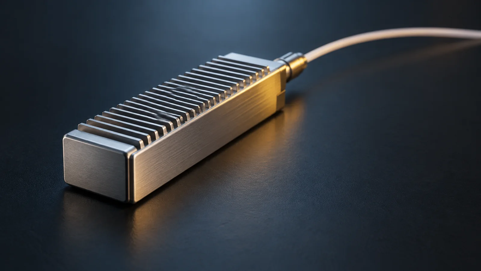
Look at the front of a data-centre switch and you see rows of small metal boxes plugged into it. Each one turns electrical signals into light and light back into electrical signals. Their shape and dimensions are fixed by industry agreements called MSAs (multi-source agreements), so a module from any vendor fits the same port. Capacity per module is moving from 800 Gb/s to 1.6 Tb/s, and the maximum power the specification allows has risen with it, from 19.8 W (first OSFP release) to 42.9 W (OSFP1600). What constrains the design of these parts today is not the light. It is heat.
- What an optical transceiver is (the short version)
- What is inside the box — moving eight electrical lanes onto light
- Who decides what — how IEEE, the MSAs and OIF divide the work
- Our calculation: reading each generation as lane count × lane rate
- Heat decides everything — how the power ceiling has risen
- A materials engineer's view (1): cooling comes down to metal faces that rub together
- A materials engineer's view (2): the real temperature limit is the laser
- What is still hard
- Glossary / References / Claim-to-source audit
Sourced = stated in a standard, a specification or a public document from a standards body (link given)
Our calculation = a figure this article derived, with the assumptions spelled out
Not yet confirmed = a standard still in development or a plan, with no confirmed approval or track record
Structural readings and materials-design interpretations are marked separately as Commentary.
1. What an optical transceiver is (the short version)
An optical transceiver is the part that turns a piece of equipment's electrical signal into an optical signal, sends it down a fibre, and turns the light that arrives back into electricity. In data centres the usual form is a module that can be plugged in and pulled out of the front panel of a switch or server. That is what is meant by a pluggable optical module.
- What it does: it connects to the host (the switch chip) over several electrical lanes and sends and receives light on the fibre side. The OSFP specification draws an 800G module as "8x100G PAM4" electrical lanes paired with eight optical transmitters and eight optical receiversSourced
- Who sets the shape: the outline, connector, power supply and cooling are defined by an MSA (an industry agreement among several companies). The best known are QSFP-DD and OSFPSourced
- Where the action is now: 800 Gb/s per module (8 lanes × 100 Gb/s) and 1.6 Tb/s (8 lanes × 200 Gb/s). Both MSAs have published specifications for 1.6 Tb/s versionsSourced
This article is about the box that plugs into the front panel itself. Getting rid of the box and moving the optical converter into the chip package is covered in our Co-packaged Optics explainer; keeping the box but stripping out what is inside it is covered in our explainer on NPO and LPO. The modulation used inside the box (PAM4 and so on) is covered in our explainer on optical modulation and modulation formats, the part that generates the light in our semiconductor lasers explainer, and the connection to the fibre in our explainer on optical connectors and fibre attach.
2. What is inside the box — moving eight electrical lanes onto light
The OSFP MSA specification includes many block diagrams of what sits inside a module. The 800G DR8 configuration, for example, is drawn like this: eight electrical signals come in from the switch-side electrical interface (800GAUI-8), are cleaned up by an "8 x 100G PAM4 CDR", and leave through eight optical transmitters into the fibre, while the receive side takes the light in through eight optical receiversSourced. MPO and similar connectors are shown on the fibre sideSourced.
An optical transmitter contains a laser to produce the light, a modulator to put the signal onto it (some designs modulate the laser directly instead), and a driver circuit to drive it. An optical receiver consists of a photodetector, which turns light into current, and a TIA (transimpedance amplifier), which converts that tiny current into a voltage and amplifies it. So a single module houses compound semiconductor (the laser), silicon (the ICs), glass (the fibre), metal (the housing) and polymer (the board and adhesives) side by side (our commentary).
The biggest value of the pluggable approach is that when one fails, you pull out that one module and replace it. The QSFP-DD MSA describes backward compatibility as "critically important", saying that being able to use existing QSFP modules in new equipment greatly lowers the risk of adoptionSourced. As our Co-packaged Optics explainer showed, CPO gives up this advantage in exchange for shorter electrical wiring. The two are less a matter of better and worse than a difference in priorities (our commentary).
3. Who decides what — how IEEE, the MSAs and OIF divide the work
A product called "an 800G optical module" is not defined by any single standard. Several bodies each define a different layer.
- IEEE 802.3 (the Ethernet standard): IEEE 802.3df-2024 is the amendment that added MAC parameters for 800 Gb/s and physical layers for 400 Gb/s and 800 Gb/sSourced. Its objectives include carrying 800 Gb/s over 8 pairs of single-mode fibre for at least 500 m and 2 km, over 8 pairs of multimode fibre for at least 50 m and 100 m, and over 8 lanes of copper twinaxial cable for at least 2 mSourced
- MSAs (agreements on the form): the QSFP-DD MSA states its aim as securing "mechanical, electrical, thermal and signal-integrity interoperability" between module components from different manufacturersSourced
- OIF: the QSFP-DD MSA website says that future updates to CMIS, the management interface specification, will be made under the auspices of the OIFSourced
IEEE standards decide how far a signal goes and with what kind of light, but not the dimensions of the box or how many watts it may dissipate. That gap is filled by the MSAs. Many of the requirements on materials and components are in fact written in the MSA specifications (our commentary).
4. Our calculation: reading each generation as lane count × lane rate
A module's capacity is essentially the number of electrical lanes × the rate per lane. Put the two MSAs' specifications side by side and each change of generation reads as that multiplication.
| Form factor | Electrical lanes | Rate per lane | Total | What the specification says |
|---|---|---|---|---|
| QSFP-DD | 8 | 50 Gb/s PAM4 | 400 Gb/s | Adds a second row of contacts to QSFP to get eight lanes |
| QSFP-DD800 | 8 | 100 Gb/s PAM4 | 800 Gb/s | Electrical operation at 112 Gb/s (56 GBd) per lane |
| QSFP-DD1600 | 8 | 200 Gb/s PAM4 | 1.6 Tb/s | 224 Gb/s (112 GBd) per lane. Backward compatible with QSFP-DD and QSFP+ |
| OSFP (OSFP800) | 8 | 100 Gb/s PAM4 | 800 Gb/s | 800GAUI-8: 112G-PAM4, 53.125 GBaud |
| OSFP1600 | 8 | 200 Gb/s PAM4 | 1.6 Tb/s | 1.6TAUI-8: 224G-PAM4, 106.25 GBaud |
| OSFP-XD | 16 | 200 Gb/s PAM4 | 3.2 Tb/s | 3.2TAUI-16. Twice the front-panel density of OSFP |
All Sourced (QSFP-DD specification Rev 7.1 [Ref. 1], QSFP-DD website [Ref. 3], OSFP specification Rev 5.22 [Ref. 4], OSFP-XD specification Rev 1.11 [Ref. 6]). The "Total" column matches what the specifications state.
The QSFP-DD specification says the form is designed so that "up to 36 modules" fit in 1U of a 19-inch rack, and the OSFP MSA likewise says "Up to 36 OSFP ports are supported in 1 U front panel"Sourced.
- 36 ports × 1.6 Tb/s = 57.6 Tb/s (per 1U of front panel)Our calculation
- 36 ports × 800 Gb/s = 28.8 Tb/sOur calculation
Assumptions and limits: 36 ports is an "up to" figure; the port count of real equipment depends on its design. Some configurations also plug copper cables (DAC or AEC) into the ports instead of optical modules.
5. Heat decides everything — how the power ceiling has risen
As capacity goes up, so does module power. The OSFP specification includes a table of the maximum power allowed in each revisionSourced.
Why the ceiling rose is written plainly in the specification. For OSFP and OSFP800, each of the four power pins can carry up to 2.5 A, for a total of 10.0 A and more than 30 W; for OSFP1600 it is 3.25 A per pin, 13.0 A in total and more than 40 WSourced. The 16-lane OSFP-XD has eight power pins, for a total of 20 A and more than 60 WSourced.
The QSFP-DD specification divides power into eight classes. Class 1 is 1.5 W, followed by 3.5, 7.0, 8.0, 10, 12 and 14 W; Class 8 is ">14 W", with the actual value read out from a management registerSourced. For hosts that support Class 8 (">~20 W"), the recommended design ties the power-pin pads through many vias to thick copper power planes so that heat is removed by conductionSourced.
The QSFP-DD MSA technical white paper (September 2023) says the power of a typical intensity-modulation/direct-detection (IMDD) module at QSFP-DD1600 "may be around 25W"Sourced.
- 25 W / 1.6 Tb/s = 25 / (1.6 × 10¹²) J/bit = about 15.6 pJ/bitOur calculation
- With 36 modules in 1U: 36 × 25 W = 900 W. At the 42.9 W specification ceiling, 36 × 42.9 W = about 1,544 WOur calculation
Assumptions and limits: 25 W is the white paper's "may be" guide figure, not a measurement of any particular product, and a real system will not necessarily fill all 36 ports with modules drawing the same power. This is a calculation to get the order of magnitude; it cannot be used to compare the power of different approaches.
The white paper says that cooling a 50 W module in 2U equipment with 64 ports is possible, depending on airflow, but also that filling all 64 ports with 50 W modules is not practical with "today's power supplies"Sourced. In other words, before the question of whether a module can be cooled, the power supply and heat of the whole system are becoming the limit (our commentary).
6. A materials engineer's view (1): cooling comes down to metal faces that rub together
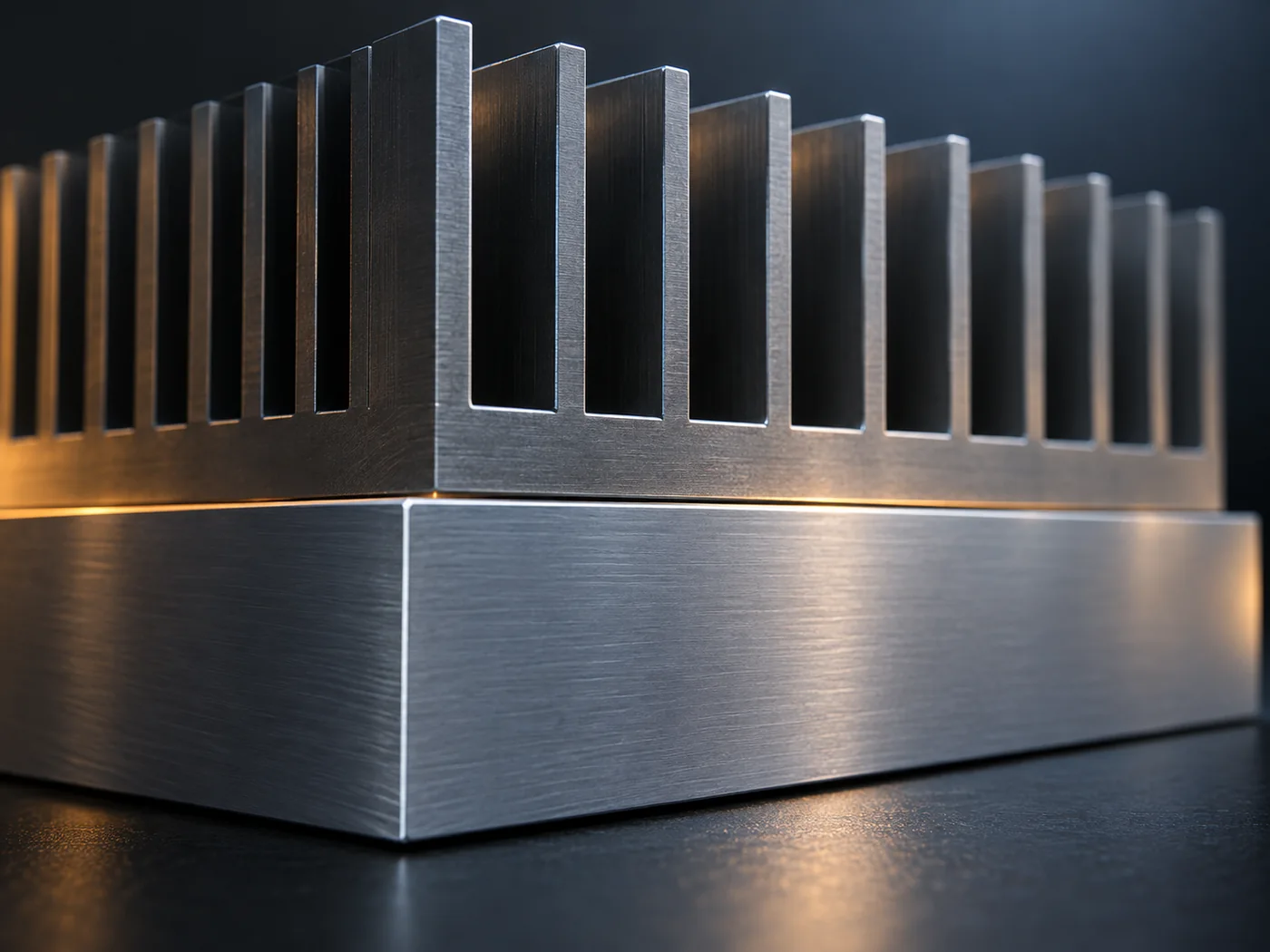
Where does the heat from a pluggable module go? The QSFP-DD MSA white paper identifies the "riding heat sink" mounted on the cage as the main path by which heat is dumped into the forced-air flowSourced. When the module is plugged in, its top face is pressed against the underside of that heat sink.
The QSFP-DD specification states explicitly that it defines module flatness and surface roughness to improve thermal performance when a "riding heat sink" is usedSourced. The higher the power class, the tighter the requirement: from Class 5 up, flatness is 0.050 mm and surface roughness Ra 0.8 µm, and the optional enhanced specification for Class 8 calls for 0.025 mm and Ra 0.4 µmSourced.
In a wind-tunnel test with a 30 W module, the white paper reports that, relative to dry metal-to-metal contact, a "TIM with durable coating" lowered module temperature by about 3 °C, and a combination of a different heat-sink design and a different TIM by 7 °C in totalSourced. It then adds that "addressing the wear and tear due to insertion cycles remains a consideration"Sourced.
This is where it gets interesting from a materials standpoint. Thermal grease on a CPU is applied once and never moves. The contact face of a pluggable module, by contrast, rubs against the underside of the heat sink every time it is inserted. The specified durability is 50 cycles for the module and 100 cycles for the connector and cageSourced.
- Thermal conduction: it should fill gaps on the order of the tens-of-micrometres flatness tolerance and cut thermal resistance
- Wear resistance: after dozens of sliding contacts against metal it must not peel, abrade or shed particles
- Cleanliness: an optical connector sits right next to it. Wear debris or volatiles landing on an optical mating face would themselves cause loss
The requirements of a thermal-conduction material and a tribological (friction and wear) material fall on the same thin film at once — an unusual combination even in the world of thermal materials (our commentary). The white paper also notes that in the QSFP-DD800 work, relatively simple optimisations, including better thermal conductivity of the housing material, contact-face flatness, housing design and thickness, and improved TIM, made a temperature reduction of 15 to 16 °C possibleSourced. The metal of the housing itself is being judged as a thermal component (our commentary).
7. A materials engineer's view (2): the real temperature limit is the laser
On where to measure the module's case temperature, the QSFP-DD specification says it should be "a point connected to an internal component with the least thermal margin, e.g., a laser diode"Sourced. The temperature classes are 0 to 70 °C standard, −5 to 85 °C extended and −40 to 85 °C industrialSourced.
The white paper goes further, pointing out that designing only to the case-temperature limit (typically 75 °C) leaves margin on the tableSourced. In its example, the margin measured against case temperature is only 2.4 °C, yet there was a further 6.2 °C before laser performance was affectedSourced.
So the thermal design of a module is not a question of what temperature to hold the box at, but of what temperature to hold the laser at. And the laser is not necessarily located anywhere near the top face of the housing.
- The internal heat path from laser to case (die-attach material, submount, internal TIM, housing thickness)
- The contact face from case to heat sink (Section 6)
- From the heat sink to the air
These three thermal resistances sit in series. The outer part (heat sink and air) is designed by the equipment maker and the inner part (laser to case) by the module maker — and the MSA specification is what draws the line over who owns the interface between them (our commentary). As our semiconductor lasers explainer covers, a laser's wavelength and efficiency both shift with temperature. Thermal materials are also materials that directly govern optical performance (our commentary).
8. What is still hard
(1) The Ethernet standard for 200 Gb/s per lane is still being written
1.6 Tb/s Ethernet using 200 Gb/s lanes is being developed as IEEE P802.3dj. Its objectives include carrying 1.6 Tb/s over 8 pairs of single-mode fibre for at least 500 m and 2 km and over 8 pairs of copper twinaxial cable for at least 1.0 m, among othersSourced. A task force document from December 2025 set out a plan that, on the most optimistic view, would go to IEEE Standards Association (SA) ballot in early 2026Sourced. As of this article's research (September 2026), the IEEE SA standards page still lists P802.3dj as under development (Active PAR), and final approval could not be confirmed from primary sourcesNot yet confirmed. The QSFP-DD specification is likewise worded to say that QSFP-DD1600 is expected to comply with IEEE 802.3dj "when published"Sourced.
(2) The ceilings on heat and power
As Section 5 showed, the specified power ceiling has risen with each revisionSourced. But as the white paper says, filling every port with high-power modules is becoming impractical on the power-supply sideSourced. Technology to cool modules and technology to reduce the power of the modules themselves have to be pursued separately. The leading examples of the latter are LPO, which drops the DSP, and NPO and CPO, which bring the optics close to the package (see our explainers on NPO and LPO and on Co-packaged Optics).
(3) There are two families of form factor
QSFP-DD and OSFP both support eight lanes and 1.6 Tb/s, but they are not interchangeable. The OSFP MSA says that OSFP and OSFP-XD are not interchangeable with each other either, owing to mechanical and electrical differencesSourced. QSFP-DD puts backward compatibility with existing QSFP firstSourced, while OSFP makes an integrated heat sink the standard form and also offers OSFP-RHS, which has no heat sinkSourced. For component and materials suppliers, this means two parallel sets of specifications for housings, heat sinks and cages (our commentary).
(4) What this article does not cover
Measured power consumption of individual products, the power breakdown by optical component (laser, modulator, photodetector) and each vendor's internal implementation are not covered, because they do not appear in the public standards and MSA documents this article could confirm. Shipment volumes and market-size estimates from research firms are not used, in line with this series' policy.
- An optical transceiver is a pluggable box that moves electrical lanes onto light. Its shape is set by the QSFP-DD and OSFP MSAsSourced
- Capacity is lane count × lane rate. 8 × 200 Gb/s = 1.6 Tb/s and 16 × 200 Gb/s = 3.2 Tb/sOur calculation
- OSFP's maximum power has risen from 19.8 W to 42.9 W (OSFP1600)Sourced, about 2.2 timesOur calculation
- At 25 W and 1.6 Tb/s, that is about 15.6 pJ/bitOur calculation
- The crux of cooling is a contact face that rubs every time the module is plugged in. Flatness tightens to as little as 0.025 mm (optional specification), and TIMs are being asked to resist wearSourced
- The real temperature limit lies in the laser. The recommended case-temperature measurement point is one connected to the laserSourced
- Final approval of the 1.6 Tb/s Ethernet standard (802.3dj) could not be confirmed as of this article's researchNot yet confirmed
9. Glossary
- Optical transceiver
- A transmit-and-receive part that converts between electrical and optical signals. In data centres, pluggable modules are the norm.
- Pluggable
- A form that can be inserted and removed for replacement while the equipment stays powered.
- MSA
- Multi-Source Agreement. An industry agreement in which several companies fix the outline, electrical and thermal characteristics and so on, so that interchangeable products can be made.
- QSFP-DD
- A form that adds a second row of contacts to QSFP to get eight lanes. There are 800G (DD800) and 1.6T (DD1600) versions.
- OSFP
- An eight-lane pluggable form with an integrated heat sink as standard. The 16-lane version is OSFP-XD.
- Lane
- A single signal stream carried on one differential pair. Module capacity = lane count × lane rate.
- PAM4
- A format that sends two bits per symbol using four amplitude levels. Covered in detail in our explainer on optical modulation and modulation formats.
- CDR / DSP
- Circuits that retime a degraded electrical signal and correct its waveform.
- TIA
- Transimpedance amplifier. A circuit that converts the tiny current from a photodetector into a voltage and amplifies it.
- Riding heat sink
- A heat sink mounted on the cage that presses against the top face of the inserted module.
- TIM
- Thermal interface material. A material that fills the gap between two faces so heat passes more easily.
- Case temperature
- The temperature at a defined point on the module housing, used as the control value in thermal design.
- CMIS
- The management interface specification for optical modules, now maintained at the OIF.
- pJ/bit
- The energy used to send one bit, in picojoules. Power divided by data rate.
10. References (primary sources)
- QSFP-DD MSA "QSFP-DD/QSFP-DD800/QSFP-DD1600 Hardware Specification for QSFP Double Density 8X Pluggable Transceivers, Revision 7.1", 25 June 2024 (PDF) — qsfp-dd.com
- QSFP-DD MSA "Enabling QSFP-DD1600 Ecosystem With Performance-Driven Thermal Innovations", technical white paper, September 2023 (PDF) — qsfp-dd.com
- QSFP-DD MSA Official website (About Us / FAQ) — qsfp-dd.com
- OSFP MSA "Specification for OSFP Octal Small Form Factor Pluggable Modules, Rev 5.22", 9 August 2025 (PDF) — osfpmsa.org
- OSFP MSA Official website (Frequently Asked Questions) — osfpmsa.org
- OSFP MSA "Specification for OSFP-XD, Octal Small Form Factor eXtra Dense Pluggable Module, Rev 1.11", 23 November 2025 (PDF) — osfpmsa.org
- IEEE 802.3 "Adopted IEEE P802.3df Objectives", 17 November 2022 (PDF) — ieee802.org
- IEEE SA "IEEE 802.3df-2024 — IEEE Standard for Ethernet Amendment 9: Media Access Control Parameters for 800 Gb/s and Physical Layers and Management Parameters for 400 Gb/s and 800 Gb/s Operation" — standards.ieee.org
- IEEE 802.3 "Adopted IEEE P802.3dj Objectives", 14 March 2024 (PDF) — ieee802.org
- IEEE P802.3dj Task Force "Timeline Consideration", 9 December 2025 (PDF) — ieee802.org
- IEEE SA "IEEE Draft Standard for Ethernet Amendment 13 ... (P802.3dj)", project page — standards.ieee.org
11. Claim-to-source audit
| Claim in the text | Basis | Label |
|---|---|---|
| That QSFP-DD, QSFP-DD800 and QSFP-DD1600 support 400 Gb/s at 8 × 50 Gb/s (or 4 × 100 Gb/s), 800 Gb/s at 8 × 100 Gb/s and 1.6 Tb/s at 8 × 200 Gb/s respectively. That DD800 operates electrically at 112 Gb/s (56 GBd) per lane and DD1600 at 224 Gb/s (112 GBd) per lane, with DD1600 expected to comply with IEEE 802.3dj "when published". That DD1600 is backward compatible with QSFP-DD and QSFP+. Power Classes 1 to 8 (1.5 / 3.5 / 7.0 / 8.0 / 10 / 12 / 14 / >14 W) and the host design recommendation for Class 8 (">~20 W", vias to thick copper power planes). That flatness and surface roughness (Classes 1 to 4: 0.075 mm, Ra 1.6 µm; Classes 5 to 8: 0.050 mm, Ra 0.8 µm; optional enhanced Class 8: 0.025 mm, Ra 0.4 µm) are specified to improve thermal performance with a riding heat sink. A heat-sink contact force of 25 N or more recommended for Class 5 and above. Contact plating of "Precious" and durability of 50 cycles for the module and 100 cycles for the connector and cage. Up to 36 modules in 1U. That the case-temperature measurement point should be one connected to the component with the "least thermal margin, e.g., a laser diode". Temperature classes (0 to 70 °C, −5 to 85 °C, −40 to 85 °C) | QSFP-DD MSA specification Rev 7.1Reference 1 http://www.qsfp-dd.com/wp-content/uploads/2024/07/QSFP-DD-Hardware-Rev7.1.pdf | Sourced |
| That the riding heat sink is the main path for heat into the forced-air flow. That a typical IMDD module at QSFP-DD1600 "may be around 25W". A case-temperature limit of typically 75 °C. The example of a 2.4 °C margin against case temperature with a further 6.2 °C before laser performance is affected. With a 30 W module, about 3 °C lower with TIM-A (durable coating) and 7 °C in total with DDHS plus TIM-B. "addressing the wear and tear due to insertion cycles remains a consideration". A 15 to 16 °C reduction in the QSFP-DD800 work through better thermal conductivity of the housing material and other measures. That 50 W modules can be cooled in a 64-port 2U system but 50 W in every port is not practical with today's power supplies. That coherent modules such as 1600ZR are mentioned | QSFP-DD MSA technical white paper (September 2023)Reference 2 http://www.qsfp-dd.com/wp-content/uploads/2023/09/2023-QSFP-DD%20MSA-ThermalWhitepaper.pdf | Sourced |
| That QSFP-DD adds a second row of contacts to QSFP to get eight lanes. That the MSA's aim is to secure "mechanical, electrical, thermal and signal-integrity interoperability". That backward compatibility is described as "critically important". The notice that future CMIS updates will be made under the OIF | QSFP-DD MSA websiteReference 3 http://www.qsfp-dd.com/ | Sourced |
| The 800G DR8 block diagram (8 x 100G PAM4 CDR, eight optical transmitters and eight optical receivers, MPO-type connectors). 800GAUI-8 (112G-PAM4, 53.125 GBaud) and 1.6TAUI-8 (224G-PAM4, 106.25 GBaud). Four power pins: for OSFP and OSFP800, 2.5 A × 4 = 10.0 A and more than 30 W; for OSFP1600, 3.25 A × 4 = 13.0 A and more than 40 W. Maximum power by revision (Rev 1.0 19.8 W, 2.0 21.1 W, 3.0 21.1 W, 4.0 33.0 W, 5.0 33.0 W, 5.2 33.0 W for OSFP and OSFP800 and 42.9 W for OSFP1600) | OSFP MSA specification Rev 5.22Reference 4 https://osfpmsa.org/assets/pdf/OSFP_Module_Specification_Rev5_22.pdf | Sourced |
| That OSFP supports 400G, 800G and 1.6T with eight lanes and that "Up to 36 OSFP ports are supported in 1 U front panel". That standard OSFP has an integrated heat sink and OSFP-RHS has none. That OSFP and OSFP-XD are not interchangeable because of mechanical and electrical differences | OSFP MSA website FAQReference 5 https://osfpmsa.org/ | Sourced |
| That OSFP-XD supports 3.2TAUI-16 with 16 lanes (224G-PAM4, 106.25 GBaud, 16 × 200 Gb/s = 3.2 Tb/s). Eight power pins, 20 A in total and more than 60 W | OSFP-XD specification Rev 1.11Reference 6 https://osfpmsa.org/assets/pdf/OSFP-XD_Specification_Rev1.11.pdf | Sourced |
| The objectives of carrying 800 Gb/s over 8 pairs of SMF for at least 500 m and 2 km, over 8 pairs of MMF for at least 50 m and 100 m, and over 8 lanes of copper twinaxial cable for at least 2 m | IEEE P802.3df objectivesReference 7 https://www.ieee802.org/3/df/proj_doc/objectives_P802d3df_221117.pdf | Sourced |
| That IEEE 802.3df-2024 is the amendment adding MAC parameters for 800 Gb/s and physical layers for 400 Gb/s and 800 Gb/s, and is an active standard approved and published in 2024 | IEEE SA standard pageReference 8 https://standards.ieee.org/ieee/802.3df/11107/ | Sourced |
| The P802.3dj objectives (1.6 Tb/s over 8 pairs of SMF for at least 500 m and 2 km, over 8 pairs of copper twinaxial cable for at least 1.0 m, and others) | IEEE P802.3dj objectivesReference 9 https://www.ieee802.org/3/dj/projdoc/objectives_P802d3dj_240314.pdf | Sourced |
| That as of December 2025 a plan was shown which, on the most optimistic view, would go to SA ballot in early 2026 | IEEE P802.3dj task force documentReference 10 https://www.ieee802.org/3/dj/public/25_1209/dambrosia_3dj_01b_251209.pdf | Sourced |
| Final approval of P802.3dj. As of this article's research the IEEE SA page shows it as under development (Active PAR), and approval could not be confirmed | A standard still in development; the timing of approval remains an outlookReference 11 https://standards.ieee.org/ieee/802.3dj/11115/ | Not yet confirmed |
| The multiplications 8 × 200 = 1,600 and 16 × 200 = 3,200 and the bar lengths in Fig. 3. 36 ports × 1.6 Tb/s = 57.6 Tb/s and 36 × 800 Gb/s = 28.8 Tb/s. 42.9 / 19.8 = 2.2. 25 W / 1.6 Tb/s = 15.6 pJ/bit. 36 × 25 W = 900 W and 36 × 42.9 W = 1,544 W | Our calculation. 25 W is the guide figure the white paper describes as "may be around", 36 ports is the specified maximum and 42.9 W is the specified ceiling; none of them is a measurement of a particular product | Our calculation |
| The general description of the internal parts of transmitters and receivers (laser, modulator, driver, photodetector, TIA). The framing that one module houses compound semiconductor, silicon, glass, metal and polymer. The framing of a three-layer division among IEEE, the MSAs and OIF. The reading that many of the requirements on materials are in the MSA specifications. The reading that a TIM must combine thermal conduction, wear resistance and cleanliness. The framing of three thermal resistances in series, with the MSA drawing the line at the interface. What two parallel families of form factor mean for component and materials suppliers | This article's own framing and commentary based on public documents. Not views expressed by any of the bodies or companies | Commentary |
| Measured power of individual products, the power breakdown by optical component, and each vendor's internal implementation | Not stated in this article, because they do not appear in the public standards and MSA documents it confirmed | Commentary |
| That Figs. 1, 2 and 5 are explanatory drawings, that Figs. 3 and 4 are drawings that include our calculation, and that the hero image and Fig. 6 are AI-generated images | A note by this article | Commentary |
Last updated 25 September 2026. Sources are limited to primary material (MSA specifications, technical white paper and official websites, public IEEE 802.3 documents and IEEE SA standard pages). Because the article includes structural readings and materials-design interpretations, those are marked as Commentary and kept separate from sourced fact. Measured power of individual products, the power breakdown by optical component and each vendor's internal implementation are not covered, because they could not be confirmed in published primary sources. IEEE P802.3dj is treated as still in development as of this article's research. All figures are for explanation. Figs. 1, 2 and 5 are vector drawings, Figs. 3 and 4 are vector drawings that include our calculation, and the hero image and Fig. 6 are AI-generated images; none of them shows the appearance, cross-section or dimensions of a real product.