COMPANY PROFILE / OPTICAL COMMUNICATIONS & PHOTONICS
Ayar Labs
The optical I/O specialist, backed by more than US$1 billion, that puts "optical chiplets" into GPU packages
Ayar Labs is a privately held U.S. company developing CPO (co-packaged optics): it places optical transmit-and-receive chips, known as optical engines, inside the package of a GPU or AI accelerator, so that chips are linked by optical fibre instead of copper. It was founded in 2015, and according to its website it has more than 200 employees and US$1.02 billion in total funding. It raised US$650 million in 2026 alone, and has said plainly that the money will go to scaling "high-volume production and test capacity". It does not publish its revenue. Using only the company's official releases and website, this profile sets out where it stands on the road from technology demonstration to volume production.
- Ayar Labs in 30 seconds, and where it stands in optical communications and photonics
- The logo and how the name is written
- Where the company sits in optical communications and photonics
- Scale (revenue is not disclosed, so we look at funding and people)
- Resources committed to optical communications and photonics
- What it has done so far
- What comes next
- What the company is aiming for in optical communications and photonics
- Map of partnerships in optical communications and photonics
- Technologies, products and services
- The risks this company carries
- Glossary, references and claim-to-source audit
1. Ayar Labs in 30 seconds, and where it stands in optical communications and photonics
California, U.S.Also Hsinchu (Taiwan), Boston and Bengaluru
(optical I/O start-up)Owns no fab; built in standard foundries and OSATs
inside the data centreScale-up between GPUs. Reach up to 2 km
260+ patents filedAs stated on its website
SuperNova (light source)The light source sits outside the package
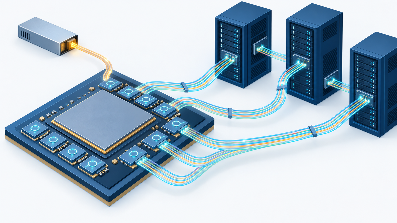
This series sorts companies in optical communications and photonics into three types: optical components & modules, chips & foundries, and network systems & carriers. Ayar Labs is an optical I/O start-up on the optical components & modules side. What it makes is not an optical transceiver but a small optical chip (a chiplet) that sits alongside a GPU or switch chip in the same package Sourced. Two features stand out. First, on the electrical side it uses UCIe, the industry standard for connecting chiplets, so that its engine can be designed into a customer's chip as a component. Second, it separates the heat-sensitive laser from the optical engine and feeds light in from an external light source called SuperNova. In short, Ayar Labs aims to turn optical transmit-and-receive into a component that fits straight into existing semiconductor design and manufacturing flows.
2. The logo and how the name is written

The Ayar Labs logo is a trademark of the company. We have not recreated it with generated imagery;
the logo image (SVG) used on the company page of the official website is placed here as img/ayar_labs_logo.svg.
A note on names: the legal entity is Ayar Labs, Inc., written with a space between "Ayar" and "Labs". Japanese-language coverage has no settled katakana rendering of the name, so this series uses the Latin-alphabet name throughout. The product names TeraPHY (optical engine) and SuperNova (light source) are both trademarks of the company.
Official site: https://ayarlabs.com/about/3. Where the company sits in optical communications and photonics
In terms of where it works with light, Ayar Labs covers connections between GPUs inside the data centre (scale-up) Sourced. Its product page says TeraPHY extends GPU-to-GPU connectivity "across tens of meters, with reach up to 2 km". It does not work on intercity long-haul transmission or LiDAR. In 2022 it also began a sensor collaboration with Lockheed Martin and a U.S. Department of Defense project, so it has a foothold in defence applications as well as AI data centres. The technologies covered in our explainers on co-packaged optics and on wavelength multiplexing and microrings are at the heart of this company.
| Aspect | Where Ayar Labs stands | Category |
|---|---|---|
| Type | Optical components & modules (optical I/O start-up). Has no fab of its own | Sourced |
| Where it works with light | Optical interconnect inside the data centre (scale-up between GPUs and accelerators). It also designs the light source (external laser) in house | Sourced |
| Where its products sit | Inside the same package as the GPU or switch (CPO). The light source is a pluggable module outside the package (ELSFP) | Sourced |
| Other applications | Defence (a U.S. Department of Defense project and a collaboration with Lockheed Martin) | Sourced |
| Long-haul and carrier networks | Not covered | Sourced |
4. Scale (revenue is not disclosed, so we look at funding and people)
Ayar Labs is privately held and does not publish revenue or profit Not yet confirmed. Instead, we show its scale through the history of its funding rounds as officially announced, and the headcount and patent filings stated on its website.
| When | Funding | Lead investor | Total raised / valuation at announcement |
|---|---|---|---|
| April 2022 | Series C, US$130 million | Boardman Bay Capital Management (HPE and NVIDIA joined as new investors) | - |
| May 2023 | Series C1, US$25 million (Series C total US$155 million) | Capital TEN | - |
| December 2024 | Series D, US$155 million | Advent Global Opportunities and Light Street Capital (AMD Ventures, Intel Capital and NVIDIA participated) | US$370 million total / over US$1 billion |
| March 2026 | Series E, US$500 million | Neuberger Berman (Alchip, MediaTek and others joined as new investors) | US$870 million total / US$3.75 billion |
| September 2026 | A further US$150 million (US$650 million in total for 2026) | Not stated. The company separately disclosed a strategic investment by Wiwynn in 2026 | US$1.02 billion total (website) |
| Item | Detail | Category |
|---|---|---|
| Founded | 2015. The company says it is built on more than a decade of silicon photonics research at MIT, UC Berkeley and CU Boulder | Sourced |
| Employees | More than 200 | Sourced |
| Patents | More than 260 filed | Sourced |
| Locations | San Jose (headquarters), Hsinchu (Taiwan, opened 2025), Boston, and Bengaluru (India; design centre announced in September 2026) | Sourced |
| Leadership | Co-founder Mark Wade is CEO (moving up from CTO in December 2023); co-founder Vladimir Stojanovic is CTO | Sourced |
| Revenue, profit and cash | Not published | Not disclosed |
The valuation the company has announced rose from "over US$1 billion" in December 2024 to US$3.75 billion in March 2026. Against the US$1 billion floor, that is about 3.75 times in roughly 15 months (because the 2024 figure was "over" US$1 billion, the actual multiple is lower than this) Our calculation. Adding September's US$150 million to the US$870 million total as of March 2026 gives US$1.02 billion, which matches the "$1.02B" on the website Our calculation. A valuation, however, is a price set by investors and says nothing about the size of revenue or profit.
5. Resources committed to optical communications and photonics
Ayar Labs does nothing but optical I/O, so all of the company's resources point at this field. Here we separate what has and has not been made public, under four headings.
| Type of resource | What it is | Category |
|---|---|---|
| People (dedicated organisation and staff) | More than 200 employees, all working in this field. Engineering teams are in the United States, Hsinchu and Bengaluru, and the VP in charge of manufacturing and operations also serves as country manager for Taiwan. Sankara Venkateswaran, formerly of Intel, became VP of engineering in February 2026 | Sourced |
| Money (investment and R&D spending) | US$1.02 billion raised in total. The Series E funds are to "scale high-volume production and test capacity, expand global operations, including at its new Hsinchu, Taiwan, office, strengthen ecosystem partnerships". R&D spending and capital expenditure are not published | Sourced / breakdown not disclosed |
| Outside investments, acquisitions and joint ventures | No investment, acquisition or joint venture by Ayar Labs in another company appears in the official releases we checked. Conversely, AMD, Intel, MediaTek, NVIDIA, Alchip, Wiwynn and others have made strategic investments in Ayar Labs | Not confirmed (it is the one receiving investment) |
| Universities, research institutes and public funding | The company's roots are in research at MIT, UC Berkeley and CU Boulder. In 2022 it won a US$15 million multi-year prototype Other Transaction Agreement (OTA) for the U.S. Department of Defense's Project KANAGAWA. In 2019 it was selected as the optical solution for Intel's DARPA PIPES project. No CHIPS Act funding has been confirmed | Sourced / CHIPS Act not confirmed |
Ayar Labs' backers include the GPU makers AMD and NVIDIA, the ASIC design houses Alchip and MediaTek, the rack-scale server maker Wiwynn, and Intel Sourced. The Series E release says the participation of MediaTek and Alchip "further strengthens Ayar Labs' alignment with key custom ASIC design ecosystem partners". An optical engine cannot be sold on its own; it only becomes a product once it is built into a GPU or ASIC package. That the companies who would build it in are also among the investors reflects the very structure of the business.
6. What it has done so far
| When | What happened | Why it matters |
|---|---|---|
| 2015 | Founded. The website lists among that year's achievements the "World's First Processor to Communicate Using Light (results published in Nature)" | A start rooted in university research |
| 2017 | Strategic partnership with GlobalFoundries | Secured a home for manufacturing |
| 2019 | Selected as the optical solution for Intel's DARPA PIPES project | Took part in a public research programme |
| 2021 | The website lists the "Industry's First 1 Tbps Optical Link for CPO". A 2022 release says the company had run its 64-wavelength WDM optical source at up to 100°C | Technology demonstrations |
| 2022 | Series C of US$130 million. Collaboration with Lumentum on the supply of external laser sources. Collaboration with Lockheed Martin. Won the U.S. Department of Defense's Project KANAGAWA (US$15 million). The website gives this as the year of its "First Volume Shipments" | The year it built both a supply chain and a defence foothold |
| March 2023 | Public demonstration of 2.048 Tbps in each direction, 4.096 Tbps bidirectional, between optical engines. Latency under 10 ns, under 5 pJ/bit (10 W), no forward error correction (FEC) | A technology demonstration. The same release also says the company is "now shipping in-package optical I/O solutions" |
| December 2023 | Co-founder Mark Wade becomes CEO | An engineer takes the helm |
| November 2024 | At SC24, shows example configurations built with Fujitsu, Intel Foundry, Corning and Altera | An exhibit, not an announcement of product adoption |
| December 2024 | Series D of US$155 million; valuation over US$1 billion | AMD, Intel Capital and NVIDIA invest |
| March 2025 | Announces a UCIe optical chiplet (TeraPHY, 8 Tbps, driven by a 16-wavelength SuperNova light source), which it calls the "world's first" | Made the engine easier to build into customers' chips |
| September 2025 | Partnership with Alchip, using TSMC's COUPE and SoIC. The same month the two jointly unveil a CPO configuration with more than 100 Tbps and more than 256 optical ports per GPU | A route to market through an ASIC design house |
| November 2025 | Partnership with GUC. Announces a design delivering more than 100 Tbps (full duplex) from an XPU multi-chip package | A second ASIC design house |
| March 2026 | Series E of US$500 million (valuation US$3.75 billion). Partnership with Wiwynn on optically connected rack-scale AI systems | Moves from components towards reference designs at rack level |
| June 2026 | Joins the NVIDIA NVLink Fusion ecosystem | Commits to products compatible with NVIDIA's optical and SerDes technology |
| September 2026 | A further US$150 million (US$650 million in total for 2026). Design centre in Bengaluru, India | The company describes a "transition from technology development to commercialization and production" |
7. What comes next
and test capacityFrom the Series E and September funding releases
Design CenterTo cover silicon product development end to end
and beyondReference design with Wiwynn; over 100 Tbps each
NVLink FusionTiming described only as aligned with customers
In the September 2026 release, the executive overseeing Bengaluru says the new design centre "supports our transition from technology development to commercialization and production" Sourced. In other words, the company itself places its current position in the transition to volume production.
None of the following appears in the official releases or on the website Not yet confirmed.
When high-volume production will start; the names of customers that have adopted its products (the releases say only "hyperscalers" or "Tier 1 customers"); revenue; production capacity; product prices; and the breakdown (customers, applications) behind the website's "Thousands of optical engines deployed". Nor does this article use the research-firm market forecasts quoted in the releases.
8. What the company is aiming for in optical communications and photonics
This section goes beyond what the company says directly. It sets out inferences that can be drawn from primary sources, each with its basis.
| What can be read | Primary evidence behind it | Category |
|---|---|---|
| The goal is to replace the copper between GPUs with light and make GPUs across several racks work as one machine | The company page and releases repeatedly describe copper's limits and speak of enabling thousands of GPUs to operate as a single unified system | Sourced |
| A strategy of getting designed in as a component by ASIC design houses and GPU makers, rather than making end products itself | Partnerships with Alchip and GUC, adoption of UCIe, participation in NVLink Fusion. ASIC design houses and GPU makers are also among its investors | Inference |
| It wants to control the light source (laser) supply chain to its own specifications | It designs SuperNova in house, collaborated with Lumentum in 2022 on volume supply, and is a promoter member of the CW-WDM MSA. It has adopted the standard ELSFP form | Inference |
| 2026 is a year of concentrating money on building volume production | Both 2026 funding releases, totalling US$650 million, name production and test capacity and manufacturing ecosystem readiness as the uses | Sourced |
| It wants to lower the barrier to adoption by offering rack-level reference designs, not just components | The Wiwynn partnership presented a rack configuration including liquid cooling, light sources and fibre management | Inference |
Between September and November 2025, Ayar Labs partnered in quick succession with two Taiwanese ASIC design houses, Alchip and GUC. Both releases describe designs that build TeraPHY into the package of a custom ASIC Sourced. The GUC design goes as far as a specific configuration: optical engines attached directly to the organic substrate of the package, linked to I/O chiplets over UCIe-S (64 Gbps), with the I/O chiplets in turn linked to the main AI die over UCIe-A (64 Gbps). When a hyperscaler builds its own AI chip, design houses like these are its point of contact for design and manufacturing. We read this as a strategy of placing its optical engine at the "front door" where chips are designed, rather than winning over customers' chips one at a time Not yet confirmed. That Alchip and MediaTek joined the Series E as investors in March 2026 is consistent with this reading.
9. Map of partnerships in optical communications and photonics
10. Technologies, products and services
A performance figure means something entirely different depending on whether it comes from a product in volume production, a sample or a demonstration. Claims of "world's first" or "industry first" are all the company's own.
| Product or technology | What it does | Main figures the company gives | Stage (as announced by the company) |
|---|---|---|---|
| TeraPHY optical engine | A silicon photonics transmit-and-receive chiplet. Uses microring modulators (MRM) and connects to the customer's chip over UCIe | Reach from tens of metres up to 2 km; 2 Tbps per mm of shoreline. The company claims 10× the bandwidth, one-tenth the latency and 3 to 5× the power efficiency of copper and pluggable optics | The website says "Multiple generations of silicon shipped. Thousands of optical engines deployed". Customer names not disclosed |
| UCIe optical chiplet (TeraPHY) | An optical chiplet with a UCIe electrical interface. The company calls it the "world's first" | 8 Tbps, driven by a 16-wavelength SuperNova light source | Announced in March 2025 |
| SuperNova light source | A laser light source placed outside the optical engine, in the industry-standard pluggable form (ELSFP) | Up to 23 dBm per wavelength, multi-wavelength, liquid-cooling compatible, compatible with the OCI-MSA standard (as the company states) | Listed as a product |
| 4 Tbps optical link | An optical link between two TeraPHY engines | 2.048 Tbps each direction (8 fibres × 8 wavelengths × 32 Gbps), latency under 10 ns, under 5 pJ/bit (10 W), no FEC | A public demonstration in March 2023 |
| Joint CPO with Alchip | A CPO configuration placing Alchip's ASIC and TeraPHY on a common substrate | More than 100 Tbps per accelerator, more than 256 optical ports | Announced in September 2025. The companies are engaging with selected customers on integration |
| Joint design with GUC | A design that places optical engines in an XPU multi-chip package | More than 100 Tbps (full duplex); UCIe-S and UCIe-A both at 64 Gbps | A design announced in November 2025 |
| Rack configuration with Wiwynn | A reference design for an optically connected, rack-scale AI system | 1,024 accelerators and beyond, more than 100 Tbps each, 100% liquid-cooled | A private preview at OFC in March 2026 |
TeraPHY's modulators are microring modulators (MRM) Sourced. A microring is a small circular waveguide that resonates with, and so picks out or modulates, only light of a particular wavelength. Being small and frugal with power, microrings suit wavelength division multiplexing (DWDM), which puts many wavelengths onto one fibre. But because the resonant wavelength is set by the refractive index of silicon, they have a weakness: even a small change in temperature shifts the wavelength. In CPO, which sits right next to the GPU, the hottest spot in the system, this becomes the central challenge.
One reading of why Ayar Labs moves the laser outside the package (SuperNova) is that lasers are also sensitive to heat, and as wear parts they are something you want to be able to replace Not yet confirmed. From a materials standpoint, thermal interface materials, underfill and substrate thermal design that even out temperature inside the package, together with the detachable fibre interface (connectors and adhesives) that brings light in from outside, affect performance as much as the optical engine itself. This is exactly what the GUC release addresses when it says that "a new stiffener design incorporates optical engines' requirements and enables detachable fiber connections while meeting mechanical stress and warpage requirements" Sourced. For more, see our explainers on wavelength multiplexing and microrings and on optical connectors and fibre attachment.
11. The risks this company carries
| Risk | Substance | Category |
|---|---|---|
| Finances not visible | As a private company it discloses none of its revenue, profit, cash or annual spending. The sustainability of its funding cannot be checked from outside | Not yet confirmed |
| High-volume production still ahead | In September 2026 the company itself described a "transition from technology development to commercialization and production". The start of high-volume production and customer names have not been announced | Sourced |
| Dependence on others for manufacturing | Photonic chip fabrication, integration into packages and assembly into racks are all left to other companies. The volume ramp depends on its partners' processes | Inference |
| Investors may also be competitors | NVIDIA, AMD, Intel and MediaTek are investors, but they are also large companies with the option of developing optical I/O themselves. An investment is not a commitment to adopt | Inference |
| Thermal design margin | Microrings are temperature-sensitive, and long-term reliability has to be shown in the hot environment right next to the GPU | Inference |
| Deep field of competitors | Optical component makers, large chip companies and other optical I/O start-ups are all working on CPO (the types in Fig. 1) | Inference |
12. Glossary
- CPO
- Co-Packaged Optics. Placing the optical engine inside the same package as the GPU or switch chip.
- Optical I/O
- Moving data between chips using light rather than electrical wiring. Ayar Labs has used this term from early on.
- Chiplet
- Instead of one large chip, several small chips divided by function and placed side by side in one package.
- UCIe
- Universal Chiplet Interconnect Express. The industry standard for connecting chiplets, which makes it easier to combine chiplets from different companies.
- Microring modulator (MRM)
- A device that modulates light of a particular wavelength using a small circular waveguide. Small and power-efficient, but sensitive to temperature.
- ELSFP
- External Laser Small Form Factor Pluggable. A standard form factor that packages the laser light source for CPO as a pluggable module.
- Scale-up
- Linking many GPUs with high speed and low latency so that they work like one large computer.
- OTA
- Other Transaction Agreement. A contracting method the U.S. Department of Defense uses, outside normal procurement rules, to move research and prototyping forward quickly.
13. References
- Ayar Labs, Inc. Official website, "About". Founded in 2015, San Jose headquarters, three regional offices, US$1.02 billion in funding, more than 200 employees, more than 260 patents filed, its roots in university research, company history (2015 to 2026), and the statement "Multiple generations of silicon shipped. Thousands of optical engines deployed." https://ayarlabs.com/about/
- Ayar Labs, Inc. Official website, "Products". Features and figures for TeraPHY and SuperNova. https://ayarlabs.com/products/
- Ayar Labs, Inc. Official website, "Leadership". Executives and co-founders. https://ayarlabs.com/leadership/
- Ayar Labs, Inc. Press release, "Lumentum And Ayar Labs Announce Strategic Collaboration To Supply External Light Sources For Co-Packaged Optical Interconnect Solutions" (9 March 2022). https://ayarlabs.com/news/lumentum-and-ayar-labs-announce-strategic-collaboration-to-supply-external-light-sources-for-co-packaged-optical-interconnect-solutions/
- Ayar Labs, Inc. Press release, "Ayar Labs Raises $130 Million in Series C Funding" (26 April 2022). https://ayarlabs.com/news/ayar-labs-raises-130-million-in-series-c-funding/
- Ayar Labs, Inc. Press release, "Lockheed Martin, Ayar Labs Partner to Advance Microchip Connectivity for Next Generation Sensory Systems" (12 October 2022). https://ayarlabs.com/news/lockheed-martin-ayar-labs-partner-to-advance-microchip-connectivity-for-next-generation-sensory-systems/
- Ayar Labs, Inc. Press release, "Ayar Labs Partners with Department of Defense to Accelerate Transition to Optical I/O in Next-Gen Defense Applications" (10 November 2022). The US$15 million multi-year prototype OTA for Project KANAGAWA. https://ayarlabs.com/news/ayar-labs-partners-with-department-of-defense-to-accelerate-transition-to-optical-i-o-in-next-gen-defense-applications/
- Ayar Labs, Inc. Press release, "Ayar Labs Demonstrates Industry's First 4-Tbps Optical Solution, Paving Way for Next-Generation AI and Data Center Designs" (1 March 2023). https://ayarlabs.com/news/ayar-labs-demonstrates-industrys-first-4-tbps-optical-solution-paving-way-for-next-generation-ai-and-data-center-designs/
- Ayar Labs, Inc. Press release, "Ayar Labs Adds $25 Million in Expansion of its $130 Million Series C" (24 May 2023). https://ayarlabs.com/news/ayar-labs-adds-25-million-in-expansion-of-its-130-million-series-c/
- Ayar Labs, Inc. Press release, "Ayar Labs Names Mark Wade CEO" (11 December 2023). https://ayarlabs.com/news/ayar-labs-names-mark-wade-ceo/
- Ayar Labs, Inc. Press release, "Ayar Labs to Showcase the Future of AI Infrastructure with Fujitsu, Intel Foundry, Corning, and Altera" (13 November 2024). https://ayarlabs.com/news/ayar-labs-to-showcase-the-future-of-ai-infrastructure-with-fujitsu-intel-foundry-corning-and-altera/
- Ayar Labs, Inc. Press release, "Ayar Labs, with Investments from AMD, Intel Capital, and NVIDIA, Secures $155 million" (11 December 2024). https://ayarlabs.com/news/ayar-labs-155m-series-d-to-address-ai-infrastructure-includes-amd-intel-capital-nvidia/
- Ayar Labs, Inc. Press release, "Ayar Labs Unveils World's First UCIe Optical Chiplet for AI Scale-Up Architectures" (31 March 2025). https://ayarlabs.com/news/ayar-labs-unveils-worlds-first-ucie-optical-chiplet-for-ai-scale-up-architectures/
- Ayar Labs, Inc. Press release, "Ayar Labs and Alchip to Scale AI Infrastructure with Co-Packaged Optics" (7 September 2025). https://ayarlabs.com/news/ayar-labs-and-alchip-to-scale-ai-infrastructure-with-co-packaged-optics/
- Ayar Labs, Inc. Press release, "Alchip and Ayar Labs Unveil Co-Packaged Optics for AI Datacenter Scale-Up" (26 September 2025). https://ayarlabs.com/news/alchip-and-ayar-labs-unveil-co-packaged-optics-for-ai-datacenter-scale-up/
- Ayar Labs, Inc. Press release, "GUC and Ayar Labs Partner to Advance Co-Packaged Optics for Hyperscalers" (16 November 2025). https://ayarlabs.com/news/guc-and-ayar-labs-partner-to-advance-co-packaged-optics-for-hyperscalers/
- Ayar Labs, Inc. Press release, "Ayar Labs Names Sankara Venkateswaran as Vice President of Engineering" (23 February 2026). https://ayarlabs.com/news/ayar-labs-names-sankara-venkateswaran-as-vice-president-of-engineering/
- Ayar Labs, Inc. Press release, "Ayar Labs Closes $500M Series E, Accelerates Volume Production of Co-Packaged Optics" (3 March 2026). https://ayarlabs.com/news/ayar-labs-closes-500m-series-e-accelerates-volume-production-of-co-packaged-optics/
- Ayar Labs, Inc. Press release, "Ayar Labs and Wiwynn Partner to Bring Co-Packaged Optics to Rack-Scale AI Systems" (11 March 2026). https://ayarlabs.com/news/ayar-labs-and-wiwynn-partner-to-bring-co-packaged-optics-to-rack-scale-ai-systems/
- Ayar Labs, Inc. Press release, "Ayar Labs Joins NVIDIA NVLink Fusion Ecosystem to Bring Co-Packaged Optics to Rack-Scale AI Infrastructure" (2 June 2026). https://ayarlabs.com/news/ayar-labs-joins-nvidia-nvlink-fusion-ecosystem-to-bring-co-packaged-optics-to-rack-scale-ai-infrastructure/
- Ayar Labs, Inc. Press release, "Ayar Labs Expands 2026 Funding to $650 Million to Scale Manufacturing-Ready CPO for AI Scale-Up Beyond the Rack" (10 September 2026). https://ayarlabs.com/news/ayar-labs-expands-2026-funding-to-650-million/
14. Claim-to-source audit
| Claim in the article | Category | Source |
|---|---|---|
| Founded in 2015, San Jose headquarters, locations, US$1.02 billion raised, more than 200 employees, more than 260 patents filed | Sourced | Reference 1 https://ayarlabs.com/about/ |
| Roots in research at MIT, UC Berkeley and CU Boulder; company history (GlobalFoundries partnership, DARPA PIPES, first volume shipments and others); "Thousands of optical engines deployed" | Sourced | Reference 1 https://ayarlabs.com/about/ |
| TeraPHY features (MRM, UCIe, up to 2 km, 2 Tbps/mm, the company's comparative claims) and SuperNova specifications | Sourced | Reference 2 https://ayarlabs.com/products/ |
| Leadership (Mark Wade as CEO, Vladimir Stojanovic as CTO, and others) | Sourced | References 3 and 10 https://ayarlabs.com/leadership/ |
| Collaboration with Lumentum on external laser sources; 64-wavelength source operating at 100°C | Sourced | Reference 4 https://ayarlabs.com/news/lumentum-and-ayar-labs-announce-strategic-collaboration-to-supply-external-light-sources-for-co-packaged-optical-interconnect-solutions/ |
| Series C of US$130 million (2022) and Series C1 of US$25 million (2023) | Sourced | References 5 and 9 https://ayarlabs.com/news/ayar-labs-raises-130-million-in-series-c-funding/ |
| Collaboration with Lockheed Martin | Sourced | Reference 6 https://ayarlabs.com/news/lockheed-martin-ayar-labs-partner-to-advance-microchip-connectivity-for-next-generation-sensory-systems/ |
| US$15 million prototype OTA for the U.S. Department of Defense's Project KANAGAWA | Sourced | Reference 7 https://ayarlabs.com/news/ayar-labs-partners-with-department-of-defense-to-accelerate-transition-to-optical-i-o-in-next-gen-defense-applications/ |
| Public demonstration of a 4 Tbps optical link (2.048 Tbps × 2, under 10 ns, under 5 pJ/bit) | Sourced | Reference 8 https://ayarlabs.com/news/ayar-labs-demonstrates-industrys-first-4-tbps-optical-solution-paving-way-for-next-generation-ai-and-data-center-designs/ |
| Exhibit at SC24 with Fujitsu, Intel Foundry, Corning and Altera | Sourced | Reference 11 https://ayarlabs.com/news/ayar-labs-to-showcase-the-future-of-ai-infrastructure-with-fujitsu-intel-foundry-corning-and-altera/ |
| Series D of US$155 million, US$370 million in total, valuation over US$1 billion | Sourced | Reference 12 https://ayarlabs.com/news/ayar-labs-155m-series-d-to-address-ai-infrastructure-includes-amd-intel-capital-nvidia/ |
| UCIe optical chiplet (8 Tbps, 16-wavelength SuperNova) | Sourced | Reference 13 https://ayarlabs.com/news/ayar-labs-unveils-worlds-first-ucie-optical-chiplet-for-ai-scale-up-architectures/ |
| Partnership with Alchip (TSMC's COUPE and SoIC) and the joint CPO configuration (over 100 Tbps, over 256 ports) | Sourced | References 14 and 15 https://ayarlabs.com/news/ayar-labs-and-alchip-to-scale-ai-infrastructure-with-co-packaged-optics/ |
| Partnership with GUC and design details (UCIe-S / UCIe-A at 64 Gbps, stiffener) | Sourced | Reference 16 https://ayarlabs.com/news/guc-and-ayar-labs-partner-to-advance-co-packaged-optics-for-hyperscalers/ |
| Appointment of Sankara Venkateswaran as VP (formerly of Intel) | Sourced | Reference 17 https://ayarlabs.com/news/ayar-labs-names-sankara-venkateswaran-as-vice-president-of-engineering/ |
| Series E of US$500 million, US$870 million in total, US$3.75 billion valuation, use of funds | Sourced | Reference 18 https://ayarlabs.com/news/ayar-labs-closes-500m-series-e-accelerates-volume-production-of-co-packaged-optics/ |
| Partnership with Wiwynn and the rack configuration (1,024 and beyond, over 100 Tbps each, liquid-cooled) | Sourced | Reference 19 https://ayarlabs.com/news/ayar-labs-and-wiwynn-partner-to-bring-co-packaged-optics-to-rack-scale-ai-systems/ |
| Joined the NVIDIA NVLink Fusion ecosystem | Sourced | Reference 20 https://ayarlabs.com/news/ayar-labs-joins-nvidia-nvlink-fusion-ecosystem-to-bring-co-packaged-optics-to-rack-scale-ai-infrastructure/ |
| The further US$150 million in 2026, Wiwynn's strategic investment, the Bengaluru design centre, the statement about the "transition from technology development to commercialization and production" | Sourced | Reference 21 https://ayarlabs.com/news/ayar-labs-expands-2026-funding-to-650-million/ |
| Change in valuation (about 3.75 times) and reconciliation of total funding (US$870 million + US$150 million = US$1.02 billion) | Our calculation | Calculated in this article from the figures in references 12, 18, 21 and 1 https://ayarlabs.com/news/ayar-labs-expands-2026-funding-to-650-million/ |
| The three types of company in optical communications and photonics | Our calculation | Our own classification. Companies shown are examples from those covered in this series |
| Revenue, profit, cash, R&D spending and capital expenditure | Not yet confirmed | None is disclosed, and this article makes no estimate https://ayarlabs.com/about/ |
| Start of high-volume production, customer names, production capacity, product prices, breakdown of the "thousands of optical engines" | Not yet confirmed | Not in references 1 to 21. Information from press reports is not used https://ayarlabs.com/about/ |
| Research-firm market forecasts quoted in the releases | Not yet confirmed | Not used, in line with this article's policy https://ayarlabs.com/news/ayar-labs-demonstrates-industrys-first-4-tbps-optical-solution-paving-way-for-next-generation-ai-and-data-center-designs/ |
| Outside investments, acquisitions and joint ventures; CHIPS Act funding | Not yet confirmed | Not in the primary sources we checked. This article does not conclude that none exists https://ayarlabs.com/about/ |
| The reading that its strategy is to be designed in as a component by ASIC design houses and GPU makers | Inference | This article's interpretation of references 14 to 16, 18 and 20 |
| The reading that it wants to control the light-source supply chain | Inference | This article's interpretation of references 2 and 4 |
| The reading that it wants to lower the barrier to adoption with rack-level reference designs | Inference | This article's interpretation of reference 19 |
| Why the laser is placed outside, and the view on thermal design and connection materials | Inference | This article's commentary based on references 2 and 16 |
| Risks of dependence on others for manufacturing, competition with investors, thermal margin and competitors | Inference | This article's interpretation of the partnership structure and technical approach |
Last updated 26 September 2026 / Troy Technical
Every figure in this article comes from the official website and official press releases of Ayar Labs, Inc. No research-firm estimates or press-based figures have been used (nor have the research-firm market forecasts quoted in the releases). Passages marked "Inference" are this article's interpretation of primary sources, not statements made by the company.