COMPANY PROFILE / OPTICAL COMMUNICATIONS & PHOTONICS
Intel
A silicon photonics pioneer that let go of optical modules and shifted to research and packaging that put light on the chip
Intel was one of the first companies to put silicon photonics into volume production. According to its own materials, it has shipped more than 8 million photonic integrated circuits (PICs) and more than 32 million on-chip lasers. Yet in October 2023 it transferred the manufacture and sale of pluggable optical transceivers, its main outlet, to Jabil. What Intel now publicises in optical communications is a prototype OCI (Optical Compute Interconnect) chiplet that puts optical input and output directly on CPUs and GPUs, and, as a contract manufacturer (Intel Foundry), research into CPO packaging technology. This profile keeps the company-wide figures to a minimum and sets out how Intel's optics business has changed and what the primary sources can confirm today.
- Intel in 30 seconds, and where it stands in optical communications and photonics
- The logo and how the name is written
- Where the company sits in optical communications and photonics
- Scale (the CPU and foundry businesses in brief)
- Resources committed to optical communications and photonics
- Track record so far
- Plans ahead
- What the company is aiming for in optical communications and photonics
- Partnership map
- Technologies, products and services
- The risks this company carries
- Glossary, references and claim-to-source audit
1. Intel in 30 seconds, and where it stands in optical communications and photonics
California, U.S.2200 Mission College Boulevard
(design, manufacturing and foundry)Its optical activity is optical interconnect inside the data centre
Over 32 million lasersFor pluggable optical transceivers at 100, 200 and 400G
in October 2023Manufacturing, sales and next-generation development all transferred
Companies involved in optical communications fall into three broad types: optical components & modules, chips & foundries, and network systems & carriers. Intel belongs to chips & foundries, but in optics it is part-way through repositioning itself from a company that sells optical modules to one that owns the technology to put light on the chip Sourced. In Jabil's October 2023 release, Intel's chief strategy officer spoke of a transition "as Intel shifts its focus to silicon photonics components for existing markets and emerging applications". The optical results Intel has published since then are a prototype OCI chiplet (2024) and CPO packaging research by Intel Foundry (2026). Meanwhile, our search of the 10-K for the year ended December 2025 found no mention of silicon photonics. Read this company on the understanding that its technical base is deep, but where the business stands today is hard to see from outside.
2. The logo and how the name is written
The Intel logo is a registered trademark of the company. We have not recreated it with generated imagery;
the image is the logo published on Intel's official website, placed here as img/intel_logo.png (scaled down for display).
A note on names: the legal entity is Intel Corporation. In 2024 announcements the optics unit was called the "Integrated Photonics Solutions (IPS) Group", research is published under "Intel Labs", and the CPO packaging research was announced under "Intel Foundry", the contract manufacturing arm. Bear in mind that different parts of Intel are behind different announcements.
Official site: https://www.intel.com/content/www/us/en/homepage.html3. Where the company sits in optical communications and photonics
In terms of which part of optics it touches, Intel's work is concentrated on optical interconnect inside the data centre Sourced. The PICs it has shipped in volume went into pluggable optical transceivers (100, 200 and 400 Gb/s) for data centre networks, and the OCI chiplet is intended for links between CPUs and GPUs and between CPUs and memory. The product page also carries material on fronthaul for 5G radio, but we could not confirm any current products or figures for it within the scope of this article.
4. Scale (the CPU and foundry businesses in brief)
The CPU and foundry businesses are not the subject here, so we note only the company's size Sourced.
| Measure (US$ million) | FY2023 | FY2024 | FY2025 |
|---|---|---|---|
| Revenue (company-wide) | 54,228 | 53,101 | 52,853 |
| R&D expense (company-wide) | 16,046 | 16,546 | 13,774 |
| Restructuring and other charges | (62) net credit | 6,970 | 2,191 |
As of 27 December 2025 the company had 85,100 employees. It reports three segments, CCG (client computing), DCAI (data centre and AI) and Intel Foundry, and the 10-K says the network and edge business (NEX) was folded into CCG and DCAI in the first quarter of 2025 Sourced.
The figures above are for the whole company. Intel does not disclose optics-related revenue, R&D spending or headcount Not yet confirmed. We also could not tell from the 10-K for FY2025 which segment the optics unit (IPS Group) belongs to. R&D expense fell by about US$2.8 billion from FY2024 to FY2025, but how the optics share changed is unknown.
5. Resources committed to optical communications and photonics
| Resource | Details | Status |
|---|---|---|
| People (dedicated teams and staff) | The Integrated Photonics Solutions (IPS) Group existed at the time of the 2024 announcement. The company says Intel Labs has pursued the research for more than 25 years. In 2026, Intel Foundry engineers presented CPO papers. Headcount is not disclosed | Organisation confirmed; headcount not disclosed |
| Money (R&D and facilities) | Company-wide R&D expense was US$13.774 billion in FY2025, with no optics figure. The 2024 announcement says a new silicon photonics fabrication process is being introduced, but the investment amount is not disclosed | Not disclosed |
| Own manufacturing base | Volume transceivers have been built on a 300 mm hybrid silicon photonics platform (2022 announcement). The company describes its "hybrid laser-on-wafer" technology, bonding III-V lasers onto the wafer, as a differentiator | Confirmed (current operating status not confirmed) |
| Investments, acquisitions and transfers | No optics-related investments or acquisitions found. On the contrary, it transferred manufacturing and sales of pluggable optical transceivers, and development of future generations, to Jabil (30 October 2023, Jabil release) | Transfer confirmed; investments and acquisitions could not be confirmed |
| Universities, research institutes, public funding | The 10-K records U.S. government funding under the CHIPS Act (an agreement with the Department of Commerce), but says nothing about whether any of it goes to optics research. At ECTC 2026 a collaboration with the U.S. National Institute of Standards and Technology (NIST) was also presented, but its subject is hybrid bonding, not optics | For optics specifically, could not be confirmed |
Intel Labs' 2022 announcement described an array of eight-wavelength DFB lasers fabricated together on a single silicon wafer, with output power uniformity of ±0.25 dB and wavelength spacing uniformity of ±6.5%, which the company says "exceed industry specifications" Sourced. The key is the order of manufacture: the diffraction gratings are formed in the silicon first, and the III-V (compound semiconductor) wafer is bonded on afterwards. Because the gratings that set the wavelength are made with the precise lithography tools of a 300 mm silicon fab, the wavelengths line up better than in conventional lasers made in 3- or 4-inch compound semiconductor fabs.
From the materials side, this is a design that keeps the hard-to-run III-V steps to a minimum and moves the precision-critical parts into silicon processing. On the other hand, reliability at the bonded interface between dissimilar materials depends on differences in thermal expansion and on bonding defects. The fact that the 2024 announcement goes out of its way to cite an on-chip laser failure rate below 0.1 FIT can be read as answering, with field data, what is often seen as the weak point of this bonding approach Not yet confirmed.
6. Track record so far
| When | What happened | What it means |
|---|---|---|
| More than 25 years ago | Intel Labs begins research on integrated photonics (as described in the 2024 announcement) | A long technical track record |
| 2016 | Launches its first silicon photonics product (as described on the product page) | Begins volume shipments to major cloud operators |
| 28 June 2022 | Intel Labs demonstrates an eight-wavelength DFB laser array on a 300 mm silicon wafer | Shows that the multi-wavelength light sources needed for CPO and OCI can be made in a volume fab |
| 30 October 2023 | Jabil announces it will take over manufacturing and sales of Intel's silicon photonics-based pluggable optical transceivers, and development of future generations. Intel says it is shifting its focus to silicon photonics components | Exits optical modules, its biggest optics product |
| January 2024 | The 10-K for the year ended December 2023 lists "silicon photonics" among the product offerings it has expanded in recent years | At this point the name still appears in the annual report |
| March 2024 / 26 June 2024 | At OFC 2024, demonstrates an OCI chiplet co-packaged with an Intel CPU running live data, with details announced in June: 4 Tb/s bidirectional, 5 pJ/bit. The chiplet is "a prototype", and Intel is "working with select customers to co-package OCI with their SOCs" | Presents a new pillar to replace optical modules |
| First quarter of 2025 | The network business (NEX) is folded into CCG and DCAI (10-K) | A reorganisation. Where the optics unit sits is not disclosed |
| 23 January 2026 | Files the 10-K for FY2025. Our search found no mention of silicon photonics | Optics has disappeared from view in the annual report |
| 2 June 2026 | Intel Foundry presents its CPO research at ECTC 2026 on its official blog, including glass fan-out couplers with detachable edge optical connectors and glass optical couplers fixed in V-grooves | A move towards selling optics as "foundry packaging technology" comes into view |
7. Plans ahead
tens of Tb/sAs stated on the product page. Timing not disclosed
The June 2024 announcement says a new silicon photonics fabrication process will reduce the die area of the on-chip lasers and optical amplifiers (SOAs) by more than 40% and their power by more than 15% Not yet confirmed. The June 2026 Intel Foundry blog positions glass substrates as a way to bring electrical and optical integration together on a single platform.
None of the following appears in the primary sources reviewed for this article Not yet confirmed.
The timing, customers and price of a commercial OCI chiplet (we found no official announcement of OCI progress after June 2024) / the start of shipments of the 200G-per-lane PIC / the operating status and investment behind the new silicon photonics process / the current place in the organisation and headcount of the IPS Group / the value of the transfer to Jabil / any external customers for Intel Foundry's CPO technology. The 2022 announcement quotes a research firm's forecast for the silicon photonics market, but it is not the company's own figure, so this article does not use it.
8. What the company is aiming for in optical communications and photonics
This section includes things the company does not say directly. We set them out as inferences within what the primary sources support, with the evidence for each.
| What the evidence suggests | Primary information it rests on | Category |
|---|---|---|
| It has exited finished optical modules and narrowed its focus to components and technology | Jabil's release of October 2023 and the Intel executive's statement in it that Intel is shifting its focus to silicon photonics components | Sourced |
| It wants to use optics both to differentiate its own CPUs and GPUs and as a service for foundry customers | OCI is described as co-packaged with an Intel CPU but able to be integrated with other SoCs. In 2026 Intel Foundry published CPO packaging research | Inference |
| Optics is in a period of low priority for the company as a whole | The 10-K for FY2025 appears to contain no mention of silicon photonics; R&D expense fell by about US$2.8 billion year on year, and restructuring charges were also booked | Inference |
| Intel Foundry wants to differentiate itself with packaging that combines optics and glass substrates | The June 2026 blog presents glass optical couplers side by side with glass substrates that can integrate electrical and optical functions | Inference |
Laying Intel's optics materials out in chronological order shows that the source of the announcements has shifted from a product division to research and to contract manufacturing Sourced. From 2016 it mass-produced optical transceivers as products, and in 2024 a product division, the IPS Group, announced OCI. The most recent announcement, in 2026, however, came as part of Intel Foundry's round-up of packaging papers, where CPO was one topic among 20 papers. We read this as a sign that Intel is repositioning optics from "a product it sells itself" to "a packaging technology it offers when building other companies' chips" Not yet confirmed. The company itself has not explained things this way, however, and it has not announced that it has stopped commercialising OCI. This remains our interpretation.
9. Partnership map
10. Technologies, products and services
| Product or technology | Published specifications | Stage |
|---|---|---|
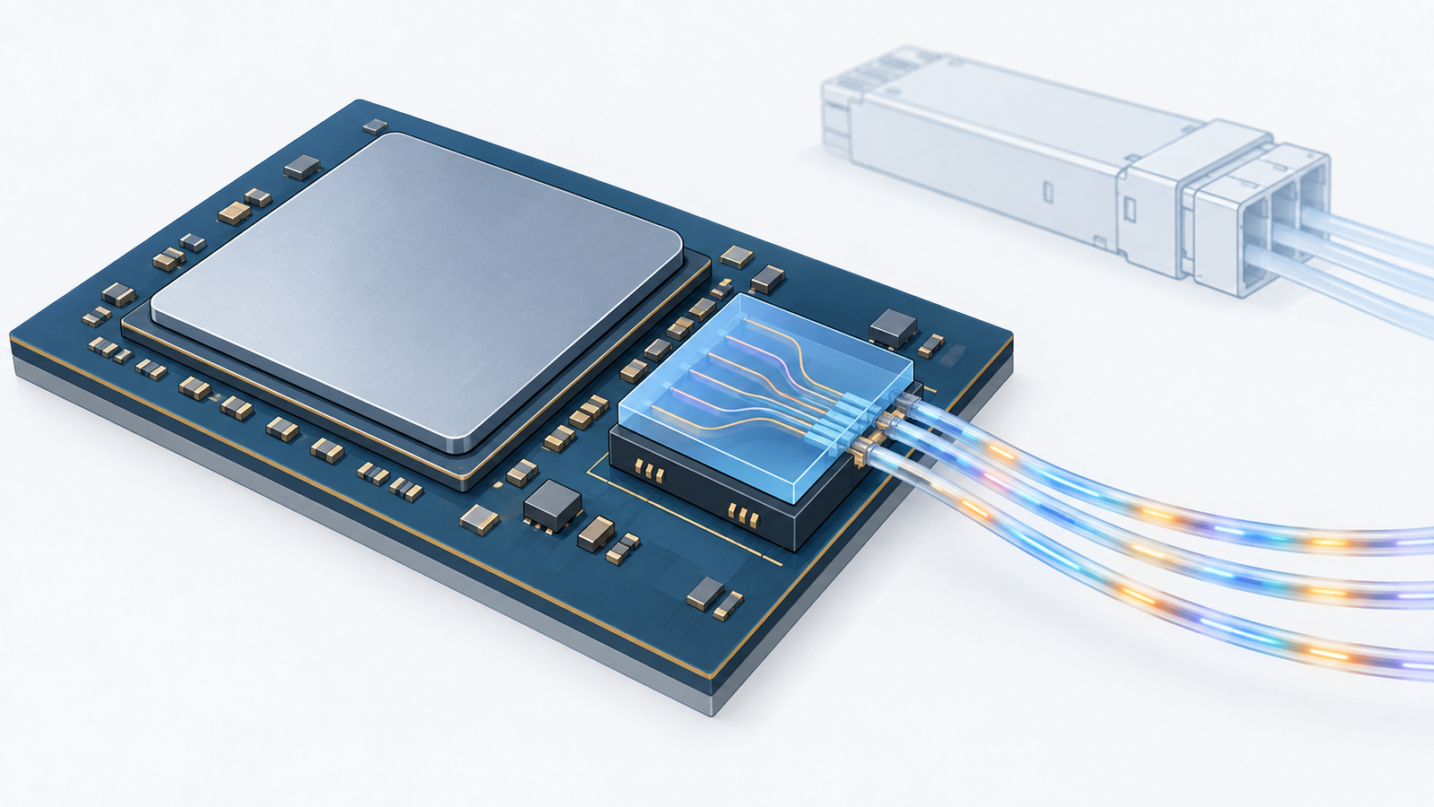
| OCI chiplet (first generation) | A silicon photonics PIC (with on-chip DWDM lasers and optical amplifiers) stacked with an electrical IC (EIC). 64 channels of 32 Gb/s in each direction, up to 4 Tb/s bidirectional. Eight fibre pairs, each carrying eight wavelengths (200 GHz spacing). Up to 100 m (tens of metres in practice). PCIe Gen5 compatible. 5 pJ/bit (the company compares this with about 15 pJ/bit for pluggables). No external light source needed; runs on standard single-mode fibre | Prototype (June 2024). Working with select customers on co-packaging |
| Silicon photonics PICs (for pluggables) | More than 8 million shipped, with more than 32 million on-chip lasers and a laser failure rate below 0.1 FIT. For 100, 200 and 400 Gb/s | Proven in volume. Product line transferred to Jabil in 2023 |
| 200G-per-lane PIC | For 800G and 1.6T | In development (as of June 2024) |
| Multi-wavelength DFB laser array | Eight wavelengths; output power uniformity ±0.25 dB; wavelength spacing uniformity ±6.5%. Made on a 300 mm hybrid silicon photonics platform | Research result (2022) |
| CPO packaging technology (Intel Foundry) | Glass fan-out couplers with expanded-beam detachable edge connectors, glass optical couplers fixed in V-grooves, and die attach by low-heat-input thermocompression bonding | Research presentation (ECTC 2026) |
"5 pJ/bit", "4 Tb/s" and "first fully integrated" are figures the company published for a prototype demonstration in 2024 Sourced. They are not specifications of a volume product. The comparison figure, "about 15 pJ/bit for pluggables", does not say which product it refers to. OCI is described as PCIe Gen5 compatible, but we could not find a clear statement in the company's primary sources about which standards (IEEE 802.3, OIF specifications and so on) the optical link itself complies with Not yet confirmed.
In its CPO research, the June 2026 Intel Foundry blog describes the conventional method of laying optical fibres directly into silicon V-grooves as a difficult and fragile process, and presents instead a method of mounting rigid glass optical couplers in the V-grooves Sourced. The same blog also cites detachable edge optical connectors using glass fan-out couplers as an approach suited to volume manufacturing.
From the materials side, glass combines properties that suit optical packaging: it resists warping with heat, is dimensionally stable and transmits light. Intel Foundry is also developing glass core substrates, and the same blog says future developments in glass substrates will allow electrical and optical integration on a single platform. The idea of holding the sub-micrometre alignment accuracy that fibre attach demands with glass rather than polymer can be read as an attempt to solve the hardest problem in CPO, the long-term stability of optical connections, through materials Not yet confirmed.
11. The risks this company carries
| Risk | Details | Category |
|---|---|---|
| The business position is not visible | The 10-K for FY2025 appears to say nothing about silicon photonics, and revenue, investment and headcount are undisclosed. We also found no OCI progress announcement after June 2024 | Sourced |
| OCI is at the prototype stage | A "prototype" as of June 2024. Timing and customers for a product are not disclosed | Sourced |
| Company-wide restructuring | Restructuring and other charges of US$6.970 billion in FY2024 and US$2.191 billion in FY2025. R&D spending is also falling | Sourced |
| It has given up its optical module outlet | The pluggable optical transceivers that built its volume track record have been transferred to Jabil. The outlets that keep its own optical production lines busy may narrow | Inference |
| Competitors reaching volume first | NVIDIA and Broadcom have announced that their CPO switches are in volume production (both companies' official announcements). Intel's optical I/O is at the prototype and research stage | Inference |
12. Glossary
- Silicon photonics
- Making optical waveguides and modulators with the process technology of silicon chip fabs.
- PIC
- Photonic integrated circuit: optical components integrated on a single chip.
- OCI
- Optical Compute Interconnect: the chiplet Intel proposes for optical input and output on CPUs and GPUs.
- DWDM
- Dense wavelength division multiplexing: sending many wavelengths (colours) of light down one fibre to increase capacity.
- DFB laser
- A semiconductor laser whose internal grating fixes it to a single wavelength. The standard light source for communications.
- SOA
- Semiconductor optical amplifier: a device that amplifies a signal while it is still light.
- FIT
- A unit of failure rate: failures per billion device hours.
- pJ/bit
- The energy used to send one bit. The smaller, the more power-efficient.
- V-groove
- A V-shaped groove used to hold optical fibres in precise positions.
- Pluggable optical transceiver
- An optical module inserted into the front panel of equipment.
13. References
- Intel Corporation Form 10-K for the fiscal year ended December 27, 2025 (filed with the U.S. SEC on 23 January 2026). Headquarters, revenue, R&D expense, restructuring and other charges, headcount, reporting segments and the folding-in of NEX, and the agreement with the government under the CHIPS Act. https://www.sec.gov/Archives/edgar/data/50863/000005086326000011/intc-20251227.htm
- Intel Corporation Form 10-K for the fiscal year ended December 30, 2023 (filed with the U.S. SEC on 26 January 2024). The passage listing silicon photonics among product offerings expanded in recent years. https://www.sec.gov/Archives/edgar/data/50863/000005086324000010/intc-20231230.htm
- Intel Corporation Press release, "Intel Labs Announces Integrated Photonics Research Advancement" (28 June 2022). The eight-wavelength DFB laser array, output power and wavelength spacing uniformity, and fabrication on a 300 mm hybrid silicon photonics platform. https://www.intc.com/news-events/press-releases/detail/1555/intel-labs-announces-integrated-photonics-research
- Intel Corporation Press release, "Intel Demonstrates First Fully Integrated Optical I/O Chiplet" (26 June 2024). OCI chiplet configuration and performance, its prototype status, PIC and laser shipment records and FIT, the next-generation PIC, the new fabrication process, more than 25 years of Intel Labs research, and the IPS Group. https://www.intc.com/news-events/press-releases/detail/1699/intel-demonstrates-first-fully-integrated-optical-io
- Intel Corporation Product page, "Intel Silicon Photonics" (accessed September 2026). OCI features (no external light source, single-mode fibre, roadmap to tens of Tb/s, evaluation platform coming), PIC and laser shipment records, and the first product in 2016. https://www.intel.com/content/www/us/en/products/details/network-io/silicon-photonics.html
- Intel Corporation (Intel Foundry) Official blog, "How Intel Foundry Packaging Technologies Redefine AI and HPC Scalability Limits at ECTC 2026" (2 June 2026). CPO research (detachable edge optical connectors, glass optical couplers in V-grooves, low-heat-input thermocompression bonding), glass substrates and electrical-optical integration, and the 20 papers. https://community.intel.com/t5/Blogs/Intel-Foundry/Systems-Foundry-for-the-AI-Era/How-Intel-Foundry-Packaging-Technologies-Redefine-AI-and-HPC/post/1749493
- Jabil Inc. Press release, "Jabil Invests in the Future of AI with Intel Silicon Photonics Transceiver Deal" (30 October 2023). Takeover of manufacturing and sales of Intel's pluggable optical transceivers and development of future generations, and a comment from Intel's chief strategy officer. https://investors.jabil.com/news/news-details/2023/Jabil-Invests-in-the-Future-of-AI-with-Intel-Silicon-Photonics-Transceiver-Deal/default.aspx
- Intel Corporation Official website (source of the company name style and the logo image). https://www.intel.com/content/www/us/en/homepage.html
14. Claim-to-source audit
| Claim in the article | Category | Source |
|---|---|---|
| Legal name, headquarters address, listing venue, 85,100 employees, reporting segments and the folding-in of NEX | Sourced | Reference 1 https://www.sec.gov/Archives/edgar/data/50863/000005086326000011/intc-20251227.htm |
| Revenue, R&D expense, restructuring and other charges (FY2023 to FY2025) | Sourced | Reference 1 https://www.sec.gov/Archives/edgar/data/50863/000005086326000011/intc-20251227.htm |
| No mention of silicon photonics found in the 10-K for FY2025 | Sourced | Result of this article's full-text search of reference 1 for "photonic", "optical", "co-packaged" and "laser" https://www.sec.gov/Archives/edgar/data/50863/000005086326000011/intc-20251227.htm |
| The 10-K for the year ended December 2023 listed silicon photonics among expanded product offerings | Sourced | Reference 2 https://www.sec.gov/Archives/edgar/data/50863/000005086324000010/intc-20231230.htm |
| The eight-wavelength DFB laser array and its fabrication method (2022) | Sourced | Reference 3 https://www.intc.com/news-events/press-releases/detail/1555/intel-labs-announces-integrated-photonics-research |
| OCI chiplet configuration and performance, its prototype status, and co-packaging work with customers | Sourced | Reference 4 https://www.intc.com/news-events/press-releases/detail/1699/intel-demonstrates-first-fully-integrated-optical-io |
| More than 8 million PICs, more than 32 million lasers, FIT below 0.1, the next-generation PIC, targets for the new process | Sourced | References 4 and 5 https://www.intc.com/news-events/press-releases/detail/1699/intel-demonstrates-first-fully-integrated-optical-io |
| First product in 2016, the OCI roadmap and the planned evaluation platform | Sourced | Reference 5 https://www.intel.com/content/www/us/en/products/details/network-io/silicon-photonics.html |
| Intel Foundry's CPO research and the positioning of glass substrates (ECTC 2026) | Sourced | Reference 6 https://community.intel.com/t5/Blogs/Intel-Foundry/Systems-Foundry-for-the-AI-Era/How-Intel-Foundry-Packaging-Technologies-Redefine-AI-and-HPC/post/1749493 |
| Transfer of the pluggable optical transceiver business to Jabil and the Intel executive's comment | Sourced | Reference 7 https://investors.jabil.com/news/news-details/2023/Jabil-Invests-in-the-Future-of-AI-with-Intel-Silicon-Photonics-Transceiver-Deal/default.aspx |
| The three types of optical communications company (optical components & modules / chips & foundries / network systems & carriers) | Our calculation | Our own classification. Example companies drawn from those covered in this series |
| R&D expense fell by about US$2.8 billion year on year | Our calculation | Calculated by this article as 16,546 minus 13,774 from reference 1 |
| Optics-related revenue, R&D spending and headcount; the IPS Group's current position; the value of the transfer to Jabil | Not yet confirmed | None of these is disclosed. This article does not estimate them either https://www.sec.gov/Archives/edgar/data/50863/000005086326000011/intc-20251227.htm |
| Timing and customers for a commercial OCI, shipments of the 200G-per-lane PIC, operating status of the new process | Not yet confirmed | Not stated in references 3 to 6. Press-based information is not used https://www.intel.com/content/www/us/en/products/details/network-io/silicon-photonics.html |
| Optics-related investments and acquisitions; optics research with universities or public funding | Not yet confirmed | Not stated in references 1 to 7. This article does not conclude that they do not exist either https://www.sec.gov/Archives/edgar/data/50863/000005086326000011/intc-20251227.htm |
| A research firm's silicon photonics market forecast | Not yet confirmed | Quoted in reference 3, but not the company's own figure, so this article does not use it https://www.intc.com/news-events/press-releases/detail/1555/intel-labs-announces-integrated-photonics-research |
| The reading that it wants to use optics both to differentiate its CPUs and GPUs and as a foundry service | Inference | This article's interpretation of references 4 and 6 |
| The reading that optics is in a period of low priority for the company as a whole | Inference | This article's interpretation of what reference 1 does and does not say, and of the trend in expenses |
| The reading that it is repositioning optics from "a product to sell" to "a packaging technology to offer" | Inference | This article's interpretation of the change in who issues announcements across references 4 to 7. The company has not explained this |
| Materials commentary on bonded lasers and glass optical couplers | Inference | This article's commentary based on the statements in references 3, 4 and 6 |
| The risks of giving up the optical module outlet and of competitors reaching volume first | Inference | This article's interpretation of reference 7 and of the two companies' official announcements covered in our NVIDIA and Broadcom profiles |
Last updated 26 September 2026 / Troy Technical
Every figure in this article comes from the statutory filings Intel Corporation has made with the U.S. Securities and Exchange Commission (SEC), from the company's official press releases, product pages and blog, and from Jabil Inc.'s official release. No research-firm estimates or press-based figures have been used. Performance figures are the company's claims and have not been independently verified. Passages marked "Inference" are this article's interpretation of the primary sources, not statements made by the company.