TECHNOLOGY EXPLAINER
Semiconductor Package Molding
Why the “black resin” is a structural material
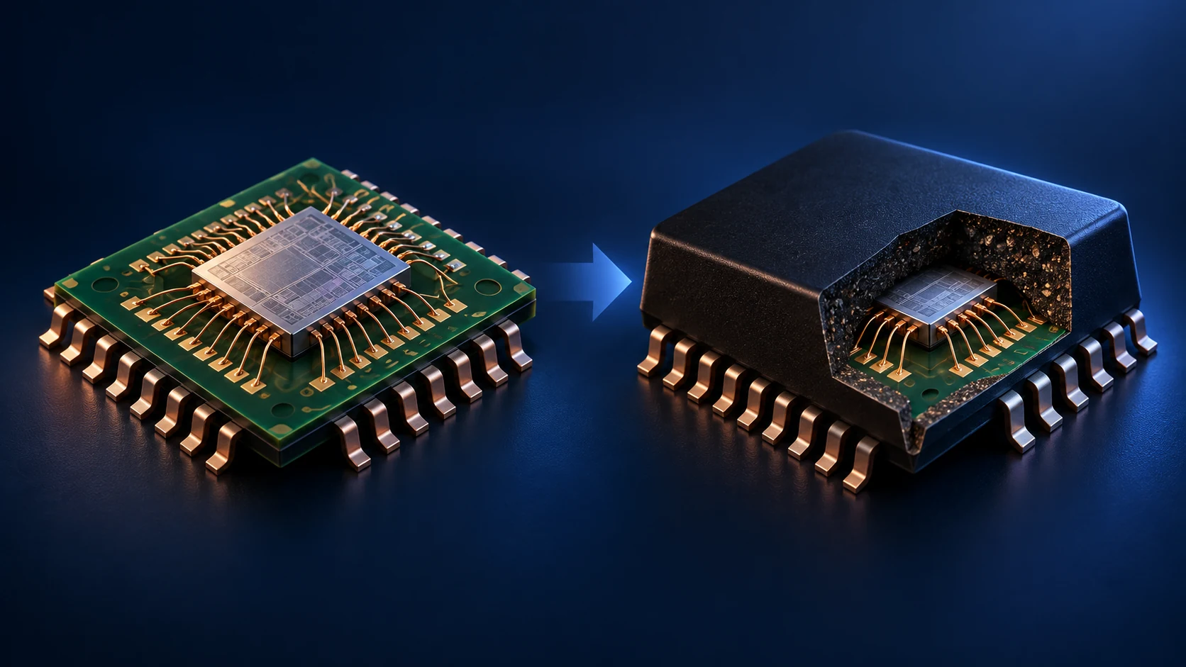
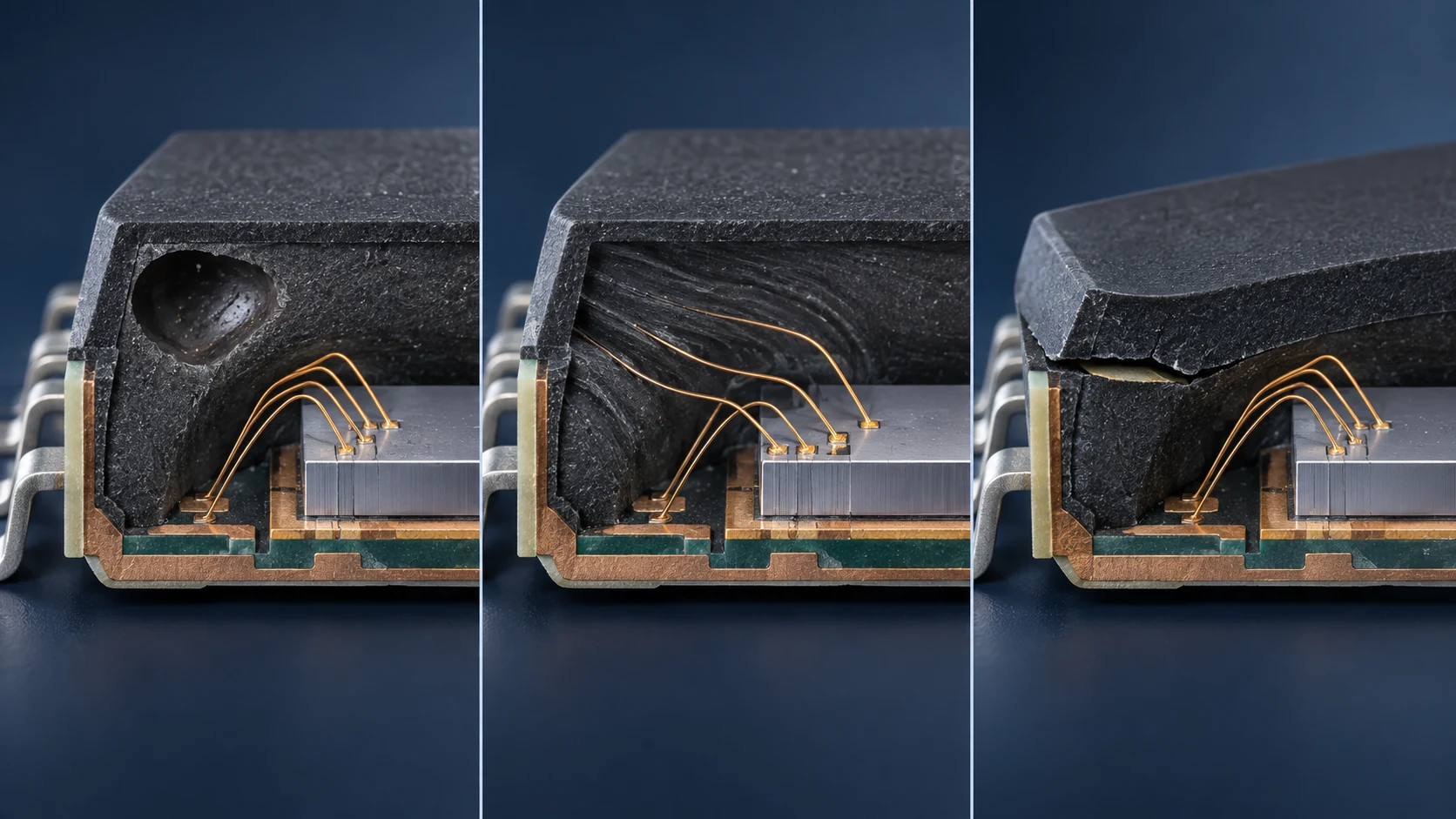
Molding surrounds dies and interconnects with a thermosetting composite that protects them from moisture, impact and thermomechanical stress. The same flow-and-cure event governs voids, wire sweep, warpage and delamination.
Sourced identifies statements or values in a primary company source. Engineering interpretation connects those facts into a practical model. Development-stage marks a stated plan rather than demonstrated mass production. All illustrations are conceptual, not equipment drawings or simulation results.
1. Molding in three sentences
Semiconductor package molding encloses a die, wires and a leadframe or substrate in a thermosetting encapsulant.
The most common material family is epoxy molding compound (EMC): epoxy resin, curing agents and inorganic fillers such as silica. Sumitomo Bakelite describes four functions for its semiconductor encapsulants—chip protection, electrical insulation from the environment, heat dissipation and package handling integrity Sourced [1].
This is not simply “pour and harden.” A useful compound must flow while the cavity is being filled and then become dimensionally and interfacially stable after cure—two opposing requirements carried by one formulation Engineering interpretation.
2. What the compound protects—and what it changes
After cure, EMC is both a skin and a load-bearing body. It immobilizes wires and the die, redirects heat, and changes how package stress is distributed. Designers therefore balance CTE, modulus, glass-transition temperature (Tg), thermal conductivity, moisture uptake and adhesion alongside dielectric and flame-retardant performance Engineering interpretation.
3. Transfer molding: driving compound through a gate
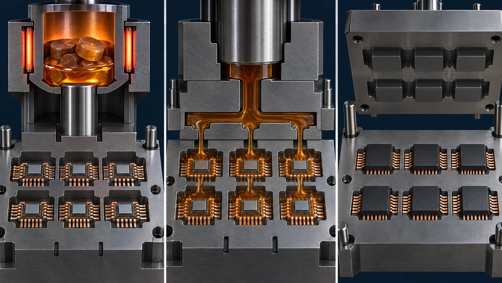
TOWA describes transfer molding as a process in which a plunger fills cavities with resin in a heated mold Sourced [2]. It is a mature way to mold many units in one shot, but it also fills runners and gates. Long lateral flow paths increase the hydrodynamic load on fine wires.
Lower viscosity helps a compound enter small features, yet velocity and pressure can still increase wire sweep, filler segregation or flash. If gelation is too early, the flow stops; if it is too late, cycle time and post-cure demands increase. The useful specification is the time-dependent viscosity window under the actual thermal history, not one viscosity value Engineering interpretation.
4. Compression molding: short flow over a large area
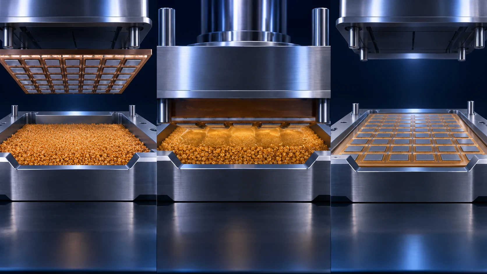
TOWA states that placing resin directly in the cavity can deliver nearly 100% material efficiency and minimize lateral resin flow, reducing its effect on dies and wires Sourced [2]. This suits thin wafer- and panel-level structures, but it moves the challenge to dispense uniformity, in-plane temperature, vacuum control, release and post-mold warpage.
| Design axis | Transfer molding | Compression molding |
|---|---|---|
| Material entry | Pot, runners and gates | Directly into the cavity |
| Dominant flow | Longer in-plane flow | More through-thickness displacement, shorter lateral flow |
| Strength | Mature, high-throughput multi-cavity production | Large area, thin structures, lower flow load on wires |
| Watchpoints | Wire sweep, gate/runner loss, end-of-fill | Compound distribution, thermal uniformity, release, warpage |
5. Designing an EMC: a highly filled composite
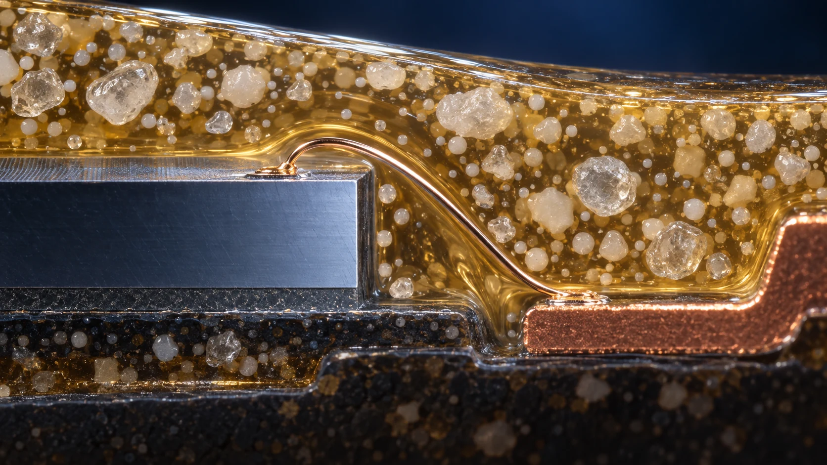
Sumitomo Bakelite describes EMC as epoxy resin combined with a curing system and inorganic fillers such as silica Sourced [3]. More filler can reduce CTE and increase stiffness or thermal conductivity, but it also affects viscosity, tool wear, narrow-gap filling and adhesion Engineering interpretation.
| Formulation lever | What it can improve | What it can compromise |
|---|---|---|
| Silica content and size distribution | Low CTE, stiffness, dimensional stability | Viscosity, gate passage, wire/tool loading |
| Alumina or other conductive filler | Thermal conductivity | Viscosity, density, wear and cost |
| Resin and curing system | Tg, adhesion, heat resistance, cure speed | Cure shrinkage, moisture uptake, storage stability |
| Interfacial treatment | Resin-to-filler and resin-to-substrate stability | Process sensitivity and humidity-aging behavior |
6. Designing the useful flow-and-cure window
A Sumitomo Bakelite FAQ gives about 60 seconds at 175°C as a typical molding condition, while noting that conditions are customized Sourced [3]. It should not be read as a universal recipe.
On heating, viscosity first falls and then rises sharply as crosslinking proceeds. Filling must finish in that valley. Tool temperature, preheat, transfer rate, pressure, vacuum and gate placement should therefore be managed around one question: how much margin separates end-of-fill from gelation? Engineering interpretation
Combine spiral flow with temperature-dependent viscosity, gel time, degree of cure, cavity-pressure traces, void content, cure shrinkage and release force under the same process history. A single material-property ranking rarely predicts the final package ranking.
7. Warpage and interface stress: CTE, Tg and modulus together
Sumitomo Bakelite publishes representative values for compression-molding grades. For example, G730 GR is listed at Tg 175°C, CTE 8/24 ppm/°C and flexural modulus 24.5 GPa; G380 GR is listed at Tg 205°C, CTE 6/25 ppm/°C and modulus 12.0 GPa Sourced [1]. These are product-specific results under stated test methods—not universal EMC targets.
Lower CTE reduces free thermal mismatch, but higher modulus can convert the remaining mismatch strain into greater stress. Both modulus and CTE change across Tg, so a package that is flat at room temperature can warp near reflow. Evaluate the full temperature path: stress is mismatch strain multiplied by the degree of constraint Engineering interpretation.
8. Common failure modes: trace the causal chain
| Observed symptom | Material-side hypotheses | Process / geometry hypotheses | Useful checks |
|---|---|---|---|
| Void / incomplete fill | Fast viscosity rise, volatiles, particle distribution | Poor venting, cold end-of-fill, gate position | CT, cross-section, pressure trace, volatile analysis |
| Wire sweep | Flow resistance, filler segregation | Velocity, gate direction, loop geometry | X-ray/CT, flow model, process DOE |
| Delamination / crack | Adhesion, moisture, cure shrinkage, modulus | Contamination, plasma treatment, corner geometry | Scanning acoustic microscopy, fractography, pretreatment split |
| Warpage | CTE, Tg, modulus, shrinkage | Thickness asymmetry, temperature gradient, cooling | Temperature-dependent warpage, DMA/TMA, FEM |
9. Advanced packaging: from protecting units to building a plane
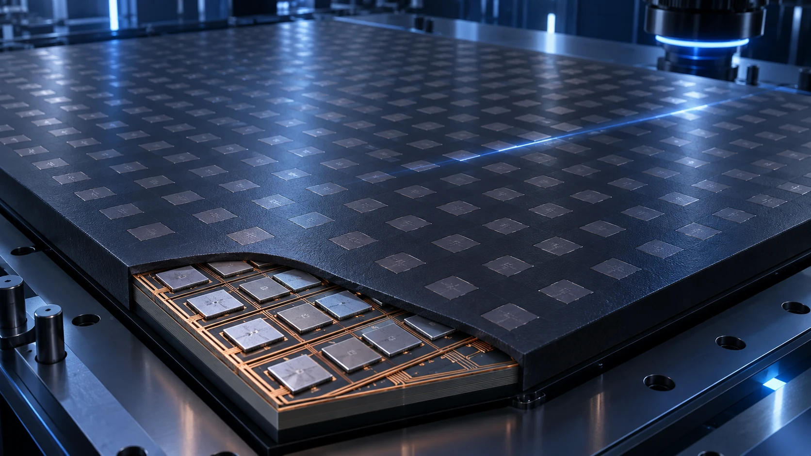
In fan-out WLP and PLP, the mold compound is not just a cover. It becomes the reconstituted wafer or panel on which redistribution layers are built. Thickness variation, die shift, warpage and flatness now affect lithography and bonding yield as directly as local voids do Engineering interpretation.
In 2026, Sumitomo Bakelite announced a low-warpage, high-reliability liquid encapsulant intended to combine under-molding and over-molding in one step. The company stated that sampling would begin in April 2026 and targeted adoption from 2027 onward Development-stage [4]. Those statements are a plan at the publication date, not evidence of mass-production adoption.
10. Selection and qualification: translate a data sheet into failure modes
- Freeze geometry: die thickness, wires or bumps, substrate, molded thickness and gate scheme.
- Define the thermal history: molding, post-cure, moisture conditioning, reflow and use temperature.
- Couple flow and cure: measure filling margin and cure state under the same conditions.
- Control interfaces independently: separate compound effects from cleaning, plasma and storage effects.
- Measure across temperature: track warpage, modulus and adhesion below and above Tg.
Material A may have lower CTE and material B lower modulus, yet either can produce the flatter package depending on stack asymmetry and mold temperature. The final decision should connect material properties → in-process state → package deformation → failure mode in one causal chain Engineering interpretation.
11. Glossary
- EMC
- Epoxy molding compound used to encapsulate semiconductor packages.
- Transfer molding
- Moving softened compound through runners and gates into heated cavities with a plunger.
- Compression molding
- Pressing a wafer or panel into compound dispensed directly in the cavity.
- Tg
- Glass-transition temperature, around which modulus and CTE can change markedly.
- CTE
- Coefficient of thermal expansion: dimensional change per unit temperature.
- Wire sweep
- Lateral deformation of bonding wires caused by mold-compound flow.
- Void
- A gas-filled or unfilled cavity remaining in the cured compound.
- Die shift
- Movement of a die during molding due to flow and pressure.
12. Primary sources and claim map
- Sumitomo Bakelite, SUMIKON® EME Epoxy Resin Molding Compounds—functions and published property values.https://www.sumibe.co.jp/english/product/it-materials/epoxy/sumikon-eme/
- TOWA, Molding Technology / Molding Equipment—transfer- and compression-molding principles and features.https://www.towajapan.co.jp/en/technology/molding/https://www.towajapan.co.jp/en/products/molding/
- Sumitomo Bakelite, FAQ for Semiconductor Materials—EMC constituents, representative mold conditions and thermal-conductivity approach.https://www.sumibe.co.jp/english/question/product/it-materials/
- Sumitomo Bakelite, “New Liquid Semiconductor Encapsulant Delivering Low Warpage and High Reliability”—2026 sample and adoption targets.https://www.sumibe.co.jp/english/topics/2026/it-materials/0514_01/index.html
- Resonac R&D Report: Granular Encapsulating Compound for Compression Molding—material design for granular compression-molding compounds.https://www.resonac.com/sites/default/files/2022-12/en_pdf-rd-report-061-61_tr03.pdf
| Claim | Basis | Status |
|---|---|---|
| Four encapsulant functions and product property examples | Source 1 | Company-published |
| Transfer/compression principles and features | Source 2 | Equipment-maker published |
| EMC constituents and typical 175°C / ~60 s condition | Source 3 | Company FAQ |
| 2026 sampling and 2027-onward adoption target | Source 4 | Forward-looking plan |
| Trade-offs, diagnostic map and selection workflow | Synthesis of the sources above | Engineering interpretation |
13. Claim-to-source audit
| Claim in the text | Type | Source |
|---|---|---|
| The four roles of the encapsulant and published property values | Sourced | Reference 1 https://www.sumibe.co.jp/english/product/it-materials/epoxy/sumikon-eme/ |
| Principles and characteristics of transfer and compression molding | Sourced | Reference 2 https://www.towajapan.co.jp/en/technology/molding/ |
| EMC composition and the typical condition of about 60 seconds at 175°C | Sourced | Reference 3 https://www.sumibe.co.jp/english/question/product/it-materials/ |
| Planned 2026 sampling and adoption targets from 2027 for a liquid encapsulant | Not yet confirmed | Reference 4 https://www.sumibe.co.jp/english/topics/2026/it-materials/0514_01/index.html |
| Granular material design for compression molding | Sourced | Reference 5 https://www.resonac.com/sites/default/files/2022-12/en_pdf-rd-report-061-61_tr03.pdf |
| Trade-offs among properties; diagnosis and selection steps | Engineering interpretation | Commentary: this article’s synthesis of the sources above |
This educational article is not a product specification or design recommendation. All illustrations are conceptual. Updated September 2026.