INSTITUTION PROFILE / ADHESIVES & ENCAPSULANTS
CHIPS Acts (EU and US)
How European and US semiconductor industrial policy indirectly touches advanced packaging materials
This profile is about a policy framework rather than a single institution. It covers the EU Chips Act (Regulation (EU) 2023/1781) and the US CHIPS and Science Act (2022). Both provide money and frameworks for semiconductor research, pilot lines and production facilities. Neither the legal texts nor the official pages we checked name adhesives or encapsulants. Even so, through advanced packaging pilot lines and materials metrology research, they touch how encapsulants, underfills and adhesives are used. We set out what was decided, who implements it, and which parts are in force or awarded and which are still proposed or open for applications.
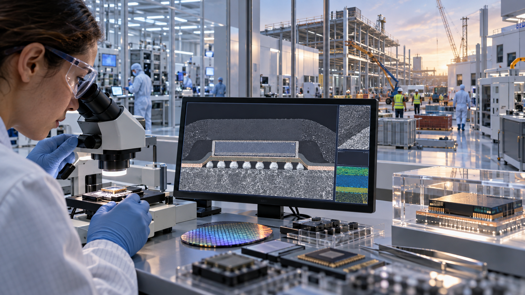
- The CHIPS Acts (EU and US) in 30 seconds
- What kind of framework it is: the four types of influence
- What was decided (and how it relates to adhesives and encapsulants)
- How far its influence reaches (powers and geography)
- Who implements it, and who is involved
- Outlook (separating in force, awarded, proposed and open)
- Glossary, references and claim-to-source audit
1. The CHIPS Acts (EU and US) in 30 seconds
US: CHIPS and Science Act of 2022The US law is Public Law 117-167 (Division A is the CHIPS Act of 2022)
US: signed 9 August 2022The EU "Chips Act 2.0" was proposed on 3 June 2026 and has not been enacted
US: $50 billion administered by CommerceThe EU figure is the text's indicative maximum. The US figure is the FY2022-FY2026 appropriation (our calculation)
US: Department of Commerce (CHIPS Program Office; R&D programmes)US R&D programmes are published on NIST's website
The CHIPS Acts are semiconductor industrial policy, not adhesive or encapsulant rules. In what we checked, adhesive and encapsulant makers are not direct recipients of funding. But money flowing into advanced packaging (assembling chips at high density) pilot lines and research can change where encapsulants, underfills and adhesives are tried out, and how they are measured. For example, NIST, within the CHIPS R&D programme, publishes a project to develop measurement methods and data for polymer packaging materials such as underfills and molding epoxies Sourced.
2. What kind of framework it is: the four types of influence
The institutions that appear in adhesives and encapsulants coverage fall into four types, according to the route by which they influence the industry. The CHIPS Acts span the two on the left, "Funding" and "Policy & regulation". But what they decide concerns the semiconductor industry as a whole, not adhesive test standards or chemical regulation.
3. What was decided (and how it relates to adhesives and encapsulants)
EU: the Chips Act (Regulation (EU) 2023/1781)
| Item | What was decided | Stage | Relevance to adhesives and encapsulants |
|---|---|---|---|
| Adoption of the regulation | Adopted by the European Parliament and the Council on 13 September 2023; published in the Official Journal (OJ L 229) on 18 September 2023 and in force on the third day after publication (21 September). Binding in its entirety and directly applicable in all member states | In force | We found no provision naming adhesives or encapsulants in the text of the regulation (our check) |
| Three pillars | (1) The Chips for Europe Initiative (capacity building and innovation); (2) security of supply and resilience (a framework for supporting first-of-a-kind production facilities); (3) monitoring and crisis response (the European Semiconductor Board) | In force | n/a |
| Funding for the Chips for Europe Initiative | For the 2021-2027 multiannual financial framework. Up to EUR 1.725 billion from Horizon Europe and up to EUR 1.575 billion from the Digital Europe Programme (both are "maximum indicative amounts" in the text), together EUR 3.3 billion (our calculation) | In force (indicative ceilings) | n/a |
| Pilot lines | According to the Commission, the Chips JU supports five pilot lines. The Chips JU lists pilot lines for 3D heterogeneous systems integration, advanced packaging and integrated photonics among its focus areas. The text names "heterogeneous systems integration and advanced module assembly and packaging" as content (Article 5) | Under way | A place where encapsulants and adhesives for advanced packaging get tried out. APECS, the EU's advanced packaging pilot line, has a total of EUR 730 million shared between the Chips JU and eight countries (as stated by Fraunhofer) |
| Support for production facilities | Sets criteria for first-of-a-kind integrated production facilities and open EU foundries. National State aid is reviewed by the Commission; its page (updated 3 June 2026) lists 18 approvals with over EUR 32 billion of public and private investment | Approved (approved cases) | The advanced packaging cases are Silicon Box (Novara, Italy, EUR 3.2 billion) and X-Fab (Erfurt, Germany, no amount given). An approval does not mean the facility is built |
| Review | The Commission must submit a report evaluating and reviewing the regulation by 20 September 2026 (Article 40) | In force (an obligation; we did not check whether it has been submitted) | n/a |
| Chips Act 2.0 | Proposed by the Commission on 3 June 2026. Among other aims, it would extend State aid for first-of-a-kind projects to "the whole semiconductor value chain, from raw materials to packaging" and set a maximum of 12 months for permitting | Proposed (not enacted) | The words "to packaging" appear, but we found nothing on adhesives or encapsulants |
US: the CHIPS and Science Act (2022)
| Item | What was decided | Stage | Relevance to adhesives and encapsulants |
|---|---|---|---|
| Enactment | Signed on 9 August 2022. In Public Law 117-167, Division A is the CHIPS Act of 2022 and Division B covers research and innovation | In force | We found no mention of adhesives or encapsulants in the text (our check) |
| Funding | Section 102 appropriates a total of $50 billion for FY2022-FY2026 to the CHIPS for America Fund: $39 billion for industry incentives (section 9902) and $11 billion for R&D (section 9906) (our addition). Commerce says the CHIPS Program Office administers $39 billion and the R&D programmes $11 billion | In force (appropriation) | n/a |
| Broader scope | Section 103 added "materials used to manufacture semiconductors" and "semiconductor manufacturing equipment" to the activities eligible for support | In force | The basis on which materials makers could qualify. From the text we could not confirm whether adhesives or encapsulants fall within it |
| Materials and equipment facilities call | The CHIPS Program Office re-opened and amended its funding opportunity for facilities for semiconductor materials and manufacturing equipment in October 2025. Concept plans are accepted until 1 November 2026 | Open | No awards have been published. We did not check the funding opportunity PDF for the range of materials covered |
| NAPMP (National Advanced Packaging Manufacturing Program) | Part of the CHIPS R&D programme. The first funding opportunity (28 February 2024), on substrates and materials R&D, finalised three awards of $100 million each, $300 million in total: Absolics (glass-core substrates), Applied Materials (silicon-core substrates) and Arizona State University (fan-out wafer- and panel-level packaging) | Awarded (first funding opportunity) | Research on substrates and materials. No adhesive or encapsulant maker is among the awardees |
| NIST measurement of packaging materials | A CHIPS R&D project, "Accurate Cure Kinetics, Stress, Mechanical Properties and Warpage". It develops measurement methods and open data on cure behaviour, thermal expansion, warpage and stress for materials including underfills and molding and potting epoxies | Under way | Bears directly on how encapsulants, underfills and adhesives are evaluated. NIST states that most of these materials are bought from overseas |
CHIPS funding goes not to encapsulant makers directly, but to those who prototype packages, make substrates and do the measuring. What decides whether an encapsulant is adopted is the evaluation result: warpage, thermal expansion, how cure progresses, degradation in humid conditions. NIST's project says it will give materials suppliers the feedback they need and create uniform test methods for assessing incoming materials. This can be read as an effort to build a common yardstick that does not rest on manufacturers' stated values. Whether it becomes an industry standard (JEDEC or otherwise) cannot be confirmed at present Not yet confirmed.
4. How far its influence reaches (powers and geography)
| Aspect | What the CHIPS Acts (EU and US) have | What they do not have |
|---|---|---|
| Powers | EU: the binding force of a regulation, research funding through the Chips JU, review of State aid (the Commission), a framework for supply crises. US: allocation of funds to facilities and R&D (Commerce), NIST's measurement research | Power to set test standards for adhesives and encapsulants. Power over chemical regulation (EU REACH, US TSCA and so on). Power to certify products |
| Geography | EU: facilities and research in the EU (competence centres have been set up in all member states and Norway). US: facilities and R&D in the US (NAPMP states the aim of establishing a domestic advanced packaging industry) | Direct power over companies or policy elsewhere. We did not check whether companies from other countries (for example Japanese firms) can take part |
| Relationship with adhesive and encapsulant makers | Customers (package and substrate makers, pilot lines) receive funding. Materials evaluation methods and data are developed | Direct subsidies to makers, or the specification of particular adhesives or encapsulants |
| Scale | EU: an indicative ceiling of EUR 3.3 billion for Chips for Europe, and over EUR 32 billion of investment covered by approved State aid. US: $50 billion administered by Commerce (NIST says about $52 billion for the whole law, and $52.7 billion on another page) | No figure is published for money spent on adhesives and encapsulants alone |
The EU's "over EUR 32 billion" is the total public and private investment in the 18 cases where State aid was approved, not EU spending. The EU's own ceiling is about EUR 3.3 billion for the Chips for Europe Initiative. The US "$50 billion" is what CHIPS for America administers; it is counted differently from the roughly $52 billion for the whole law (and $52.7 billion on another NIST page). Also, an approval or an award does not mean that the facility or research is complete. No figure for adhesives and encapsulants alone has been published, in either the EU or the US Not yet confirmed.
5. Who implements it, and who is involved
| Body or organisation | Role | Source |
|---|---|---|
| European Commission | Proposes the regulation, reviews State aid and leads the European Semiconductor Board. It also proposed the Chips Act 2.0 | Commission's Chips Act page |
| Chips Joint Undertaking (Chips JU) | A public-private partnership of the EU, participating states and private members (AENEAS, EPoSS, INSIDE Industry Association). Implements operational objectives 1 to 4 of Chips for Europe (design, pilot lines, quantum, competence centres). Its Electronic Components and Systems R&I programme also supports development of materials and equipment | Chips JU website; Article 12 of the regulation |
| Fraunhofer (IZM and others) | IZM takes part in APECS, the advanced packaging and heterogeneous integration pilot line, through high-precision integration, substrate prototyping and chiplet research | Fraunhofer IZM's APECS page (see also our Fraunhofer profile) |
| US Department of Commerce, CHIPS Program Office | Administers the $39 billion of industry incentives. Runs the call for materials and equipment facilities | NIST's CHIPS for America page |
| CHIPS R&D programmes (NIST website) | NAPMP, the metrology programme and others. NIST runs the packaging-materials measurement project | NIST's R&D programmes page |
| Absolics, Applied Materials, Arizona State University | Awardees of the first NAPMP funding opportunity ($100 million each) | NIST's NAPMP funding opportunity page |
* We could not confirm, from primary sources, a direct relationship with the companies profiled in this series (Henkel, Resonac, Sumitomo Bakelite and others).
6. Outlook (separating in force, awarded, proposed and open)
| What can be read from the sources | Primary evidence | Type |
|---|---|---|
| If the EU Chips Act 2.0 is enacted, support for first-of-a-kind projects would extend "from raw materials to packaging" | Proposed by the Commission on 3 June 2026. It needs to go through the European Parliament and the Council, and the content may change | Not yet confirmed (proposal) |
| Whether the US materials and equipment facilities call will produce awards is unknown | Concept plans are accepted until 1 November 2026. No awards have been published | Not yet confirmed (open call) |
| The effect on adhesive and encapsulant makers is likely to remain indirect, through advanced packaging pilot lines and materials measurement and data, rather than through direct subsidies | The words do not appear in the regulation, the US law or the official pages; NIST's measurement project; the content of APECS and NAPMP | Inference |
| If NIST's measurement methods and data become a common evaluation method in the industry, the basis for comparing manufacturers' stated values could change | NIST lists "uniform test methods" and "open data" among its outputs. Whether it becomes an industry standard is not confirmed | Inference |
7. Glossary
- Regulation (EU)
- A type of EU legal act. The text of the Chips Act states that it is binding in its entirety and directly applicable in all member states.
- Chips JU
- The Chips Joint Undertaking: a public-private partnership of the EU, participating states and industry, responsible for implementing the Chips for Europe Initiative.
- Pilot line
- Experimental and validation facilities between the laboratory and mass production. The regulation defines them as experimental projects at technology readiness levels 3 to 8.
- Advanced packaging
- Assembling many chips tightly together on a substrate in two or three dimensions.
- NAPMP
- The National Advanced Packaging Manufacturing Program, one of the US CHIPS R&D programmes.
- State aid
- Aid that a member state gives to companies. In the EU, the European Commission reviews its effect on the internal market and approves it.
8. References
- EUR-Lex Regulation (EU) 2023/1781 of 13 September 2023 (Chips Act), full text (OJ L 229, 18 September 2023; Articles 1, 3, 5, 11-14, 40 and 41, and the definitions). https://eur-lex.europa.eu/legal-content/EN/TXT/?uri=CELEX%3A32023R1781
- European Commission European Chips Act (three pillars, entry into force on 21 September 2023, five pilot lines, the list of 18 State aid decisions and over EUR 32 billion in investment, the European Semiconductor Board). https://digital-strategy.ec.europa.eu/en/policies/european-chips-act
- European Commission Chips Act 2.0 (main objectives; results of the original Chips Act). https://digital-strategy.ec.europa.eu/en/policies/chips-act-2
- European Commission Proposal for the Chips Act 2.0 (published 3 June 2026; confirms it is at the proposal stage). https://digital-strategy.ec.europa.eu/en/library/proposal-chips-act-20
- Chips Joint Undertaking Chips for Europe Initiative (focus areas of the pilot lines, design platform, competence centres). https://www.chips-ju.europa.eu/Chips-for-Europe
- Chips Joint Undertaking Home page (composition of the public-private partnership; ECS R&I supports materials and equipment development). https://www.chips-ju.europa.eu/
- Fraunhofer-Gesellschaft Finances (APECS total of EUR 730 million, funded by the Chips JU and eight countries). https://www.fraunhofer.de/en/about-fraunhofer/profile-structure/facts-and-figures/finances.html
- Fraunhofer IZM APECS pilot line (part of the EU Chips Act; IZM's role). https://www.izm.fraunhofer.de/en/institut/ausstattung/apecs-pilot-line.html
- US Government Publishing Office Public Law 117-167 (CHIPS and Science Act; 9 August 2022; the appropriations in section 102 and the amended definition in section 103). https://www.govinfo.gov/content/pkg/PLAW-117publ167/html/PLAW-117publ167.htm
- US Department of Commerce (NIST) CHIPS for America ($50 billion to Commerce, $39 billion for the CHIPS Program Office, $11 billion for R&D). https://www.nist.gov/chips
- US Department of Commerce (NIST) CHIPS for America Funding Updates (signed 9 August 2022, about $52 billion, Commerce administers $50 billion). https://www.nist.gov/chips/funding-updates
- US Department of Commerce (NIST) CHIPS Incentives Funding Opportunities ($52.7 billion, $39 billion, history of the funding opportunities). https://www.nist.gov/chips/chips-incentives-funding-opportunities
- US Department of Commerce (NIST) Notice of Funding Opportunity: Facilities for Semiconductor Materials and Manufacturing Equipment (re-opened and amended October 2025; concept plans accepted until 1 November 2026). https://www.nist.gov/chips/incentives-funding-opportunities/notice-funding-opportunity-semiconductor-materials-equipment
- US Department of Commerce (NIST) CHIPS Research & Development Programs (aims of R&D, $11 billion, NAPMP and metrology programmes). https://www.nist.gov/chips/research-development-programs
- US Department of Commerce (NIST) National Advanced Packaging Manufacturing Program (description of advanced packaging; the $300 million of the first funding opportunity). https://www.nist.gov/chips/research-development-programs/national-advanced-packaging-manufacturing-program
- US Department of Commerce (NIST) NAPMP Materials and Substrates R&D funding opportunity (28 February 2024; three awardees at $100 million each). https://www.nist.gov/chips/r%2526d-funding-opportunities/notice-funding-opportunity-chips-national-advanced-packaging
- US Department of Commerce (NIST) Accurate Cure Kinetics, Stress, Mechanical Properties and Warpage (metrology project on polymer packaging materials). https://www.nist.gov/programs-projects/accurate-cure-kinetics-stress-mechanical-properties-and-warpage
9. Claim-to-source audit
| Claim in the text | Type | Source |
|---|---|---|
| Adoption date, Official Journal date and entry into force of Regulation (EU) 2023/1781 (Article 41); binding force and direct applicability | Sourced | Reference 1 https://eur-lex.europa.eu/legal-content/EN/TXT/?uri=CELEX%3A32023R1781 Reference 2 https://digital-strategy.ec.europa.eu/en/policies/european-chips-act |
| The three pillars, five pilot lines, 18 State aid decisions with over EUR 32 billion of investment, the advanced packaging cases (Silicon Box, X-Fab), the European Semiconductor Board | Sourced | Reference 2 https://digital-strategy.ec.europa.eu/en/policies/european-chips-act |
| Funding ceilings of the Chips for Europe Initiative (EUR 1.725 billion and EUR 1.575 billion), its period, the five operational objectives, the content in Article 5, the implementation arrangements in Article 12, the review in Article 40 | Sourced | Reference 1 https://eur-lex.europa.eu/legal-content/EN/TXT/?uri=CELEX%3A32023R1781 |
| Composition of the Chips JU, focus areas of the pilot lines, the ECS R&I support for materials and equipment | Sourced | Reference 5 https://www.chips-ju.europa.eu/Chips-for-Europe Reference 6 https://www.chips-ju.europa.eu/ |
| The APECS total of EUR 730 million and its split between the Chips JU and eight countries; IZM's role | Sourced | Reference 7 https://www.fraunhofer.de/en/about-fraunhofer/profile-structure/facts-and-figures/finances.html Reference 8 https://www.izm.fraunhofer.de/en/institut/ausstattung/apecs-pilot-line.html |
| Chips Act 2.0 (proposed 3 June 2026; main objectives; "from raw materials to packaging") | Sourced | Reference 3 https://digital-strategy.ec.europa.eu/en/policies/chips-act-2 Reference 4 https://digital-strategy.ec.europa.eu/en/library/proposal-chips-act-20 |
| Signing date of the CHIPS and Science Act, the structure of Divisions A and B, the section 102 appropriations, the broadened scope in section 103 | Sourced | Reference 9 https://www.govinfo.gov/content/pkg/PLAW-117publ167/html/PLAW-117publ167.htm |
| Commerce's $50 billion, $39 billion and $11 billion; the statements of about $52 billion ($52.7 billion) | Sourced | Reference 10 https://www.nist.gov/chips Reference 11 https://www.nist.gov/chips/funding-updates Reference 12 https://www.nist.gov/chips/chips-incentives-funding-opportunities |
| The materials and equipment facilities funding opportunity (re-opened and amended; concept-plan deadline) | Sourced | Reference 13 https://www.nist.gov/chips/incentives-funding-opportunities/notice-funding-opportunity-semiconductor-materials-equipment |
| Structure of the CHIPS R&D programmes (NAPMP, metrology and others) | Sourced | Reference 14 https://www.nist.gov/chips/research-development-programs |
| NAPMP description; the $300 million of the first funding opportunity and its awardees (Absolics, Applied Materials, Arizona State University) | Sourced | Reference 15 https://www.nist.gov/chips/research-development-programs/national-advanced-packaging-manufacturing-program Reference 16 https://www.nist.gov/chips/r%2526d-funding-opportunities/notice-funding-opportunity-chips-national-advanced-packaging |
| NIST's packaging-materials metrology project (underfills, molding and potting epoxies, adhesives: measurement methods and data) | Sourced | Reference 17 https://www.nist.gov/programs-projects/accurate-cure-kinetics-stress-mechanical-properties-and-warpage |
| The words "adhesive", "encapsulant" and "underfill" do not appear in the EU Regulation or in the US law and official pages checked | Our calculation | Our own text search of References 1 to 3 and 9 to 16 (Reference 17 does mention underfills and adhesives) |
| The Chips for Europe total of EUR 3.3 billion and the totals of the US appropriations ($50 billion, $39 billion, $11 billion) | Our calculation | Our own addition of the amounts in References 1 and 9 |
| The four-type classification, and placing the CHIPS Acts across "Funding" and "Policy & regulation" | Our calculation | Our own classification (this article) |
| The CHIPS Acts have no power over test standards, chemical regulation or certification for adhesives and encapsulants | Our calculation | Our own reading of References 1 and 9, and of REACH and TSCA being separate laws |
| Funding does not reach encapsulant makers directly | Our calculation | Our own reading of References 14 to 17: no manufacturer of encapsulants or adhesives is among the awardees |
| Amounts or awards limited to adhesives and encapsulants | Not yet confirmed | Not stated in References 1 to 17; we do not estimate them (this article) |
| Adoption and final content of the Chips Act 2.0 | Not yet confirmed | References 3 and 4 describe a proposal; we do not estimate the outcome (this article) |
| Awards under the materials and equipment facilities call, and the range of materials it covers | Not yet confirmed | Reference 13 shows the call open and no awards; the funding opportunity PDF was not checked (this article) |
| Whether NIST's measurement methods become an industry standard | Not yet confirmed | Not stated in Reference 17; we do not estimate it (this article) |
| The third and fourth outlook items in Chapter 6 | Inference | Our own interpretation of References 1, 9 and 15 to 17 |
Last updated: 3 October 2026 / Troy Technical
Amounts and dates in this article come from EUR-Lex, the European Commission, the Chips JU, US federal law, the US Department of Commerce (NIST website) and Fraunhofer. Items marked "Inference" are our own reading of the primary sources.