COMPANY PROFILE / ADHESIVES & ENCAPSULANTS
Resonac
Created by the merger of the former Showa Denko and Hitachi Chemical, and now earning its keep in semiconductor back-end materials
Resonac comes up in any talk of adhesives and encapsulants because it is one of the few companies that holds, in one portfolio, semiconductor-package encapsulants (epoxy molding compounds and liquid encapsulants), die bonding films and thermal sheets. According to its securities report for the year to December 2025, sales revenue in the Semiconductor and Electronic Materials segment was ¥506.3 billion (up 13.7% year on year), with core operating profit of ¥108.4 billion. In the first half of 2026, sales of semiconductor back-end materials reached ¥160.0 billion, up 46% on the same period a year earlier. This profile sets out, from primary sources only, what the company puts into adhesives and encapsulants, who it works with, and how much it discloses.
- Resonac in 30 seconds, and where it stands in adhesives and encapsulants
- The logo and how the name is written (and the link to Showa Denko and Hitachi Chemical)
- Where the company sits in the field
- Scale
- Resources committed to adhesives and encapsulants
- What it has done so far
- What comes next
- What the company is aiming for in adhesives and encapsulants
- Map of partnerships in adhesives and encapsulants
- Technologies, products and services
- The risks this company carries
- Glossary, references and claim-to-source audit
1. Resonac in 30 seconds, and where it stands in adhesives and encapsulants
(secondary: functional chemicals)Petrochemicals are being separated out
photosensitive dry films, TIMACF (anisotropic conductive film) is also in the product list
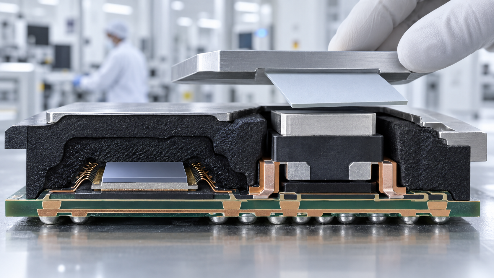
Resonac's adhesives and encapsulants are a family of materials matched to the steps of making a semiconductor package. The securities report lists, as back-end materials, epoxy molding compounds, die bonding materials (DAF and NCF), copper-clad laminates, photosensitive dry films, photosensitive solder resists and high-thermal-conductivity materials (TIM) Sourced. In other words, the steps of a package are all there: fixing the chip (die bonding), enclosing it (encapsulation), carrying heat away (TIM) and making the foundation for wiring (copper-clad laminates and photosensitive materials). This is not a company that sells a general adhesive that "bonds anything"; it is better understood as a company that co-develops materials with semiconductor customers around their processes Our calculation.
2. The logo and how the name is written (and the link to Showa Denko and Hitachi Chemical)
A note on names: the legal entity is Resonac Holdings Corporation, a holding company. The operating business is run by its subsidiary Resonac Corporation (formerly Showa Denko Materials Co., Ltd., and before that Hitachi Chemical Co., Ltd.), a separate legal entity. According to the history in the securities report, Showa Denko acquired Hitachi Chemical in April 2020 and moved to a holding-company structure in January 2023, renaming itself Resonac. Businesses once known under the "Hitachi Chemical" name, such as semiconductor encapsulants and die bonding films, are therefore now run under the Resonac name. Which individual products came from which predecessor, however, could not be confirmed from primary sources. The logo image was taken from the header of the company's official website.
Official site: https://www.resonac.com/jp3. Where the company sits in the field
4. Scale
Resonac has five segments. Its adhesives and encapsulants sit mainly in the semiconductor back-end materials business of the Semiconductor and Electronic Materials segment, so the company as a whole is covered briefly Sourced.
| Indicator (¥ million, IFRS) | Year to Dec 2024 | Year to Dec 2025 | Change |
|---|---|---|---|
| Consolidated sales revenue | 1,391,480 | 1,347,125 | -3.2% |
| Consolidated core operating profit | 92,145 | 109,145 | +18.4% |
| Semiconductor & Electronic Materials sales revenue | 445,139 | 506,336 | +13.7% |
| Semiconductor & Electronic Materials core operating profit | 73,718 | 108,365 | +47.0% |
| Consolidated employees (year end) | 23,936 | 21,525 | n/a |
The Semiconductor and Electronic Materials segment had 8,439 employees at the end of 2025 (about 39% of the consolidated total; our calculation). In the first half of 2026 (January to June), the segment's sales revenue was ¥299.0 billion (up 30% year on year) and core operating profit was ¥81.5 billion (up 92%). The breakdown is as follows Sourced.
| Semiconductor & Electronic Materials breakdown (¥ 100 million) | Jan to Jun 2025 | Jan to Jun 2026 | Change |
|---|---|---|---|
| Semiconductor back-end materials | 1,096 | 1,600 | +46% |
| Semiconductor front-end materials | 406 | 456 | +12% |
| Device solutions (HD media, SiC epitaxial wafers) | 560 | 634 | +13% |
| Other | 245 | 300 | +23% |
| Total | 2,307 | 2,990 | +30% |
The ¥160.0 billion of back-end materials includes encapsulants, die bonding materials, copper-clad laminates, photosensitive dry films, TIM and more. Sales for encapsulants and bonding products alone are not disclosed. This article does not estimate them Not yet confirmed. The back-end figure also comes from the half-year results briefing; the securities report does not give a full-year 2025 figure for back-end materials alone.
5. Resources committed to adhesives and encapsulants
Amounts and headcounts can be read at the level of "Semiconductor and Electronic Materials" or "back-end materials". There are no figures for encapsulants and bonding products alone.
| Resource | What primary sources confirm | Category |
|---|---|---|
| People | The Semiconductor and Electronic Materials segment had 8,439 employees (end of 2025). Consolidated R&D spending was ¥46,458 million, of which the segment accounted for ¥22,747 million (about 49% of the total; our calculation). R&D headcount is not disclosed | Sourced / partly undisclosed |
| Money (capital expenditure) | Capital expenditure in the year to December 2025 was ¥112.8 billion consolidated, of which the segment accounted for ¥64.1 billion. The full-year 2026 forecast for the segment is ¥78.4 billion. In 2025 the company added capacity for its integrated dicing and die bonding film, copper-clad laminates for package substrates and CMP slurry. The securities report also describes added capacity for NCF and thermal sheets (TIM), without amounts or capacities | Sourced / outlook |
| Acquisitions, investments, joint ventures | Hitachi Chemical was acquired in 2020. An affiliate is HD MicroSystems (U.S., semiconductor polyimide, 50% stake). In April 2025 the company agreed a strategic alliance with PulseForge of the U.S. on a photonic debonding process. No new acquisition in adhesives and encapsulants could be confirmed | Sourced |
| Universities, institutes, public funding | A project on 3D integration was selected under the Japan Science and Technology Agency (JST) "Next-Generation Edge AI Semiconductor R&D Program", with Yokohama National University as the lead institution. The partner institutions are Resonac, Keio University, Institute of Science Tokyo and Waseda University (announced December 2025). The amount could not be confirmed | Sourced / amount not confirmed |
| R&D and evaluation sites | The research laboratory in Tsukuba, the Packaging Solution Center in Kawasaki, the Advanced Panel Level Interposer Center (APLIC) inside the Shimodate site (Minami-Yuki), and the US-JOINT site in Silicon Valley | Sourced |
The securities report describes the company's R&D strengths as three kinds of chemistry: "making chemistry" (mid-stream materials), "mixing chemistry" (formulation matched to downstream applications) and "thinking chemistry" (evaluation, simulation and computational science) Sourced. For encapsulants and bonding films, the formulation itself (resin, filler and additives) sets performance. In the company's liquid-encapsulant patent, for example, the resin and additives are improved so that thermal expansion and elastic modulus fall within set ranges, which is said to suppress cracking in reflow and temperature-cycling tests Sourced. The R&D section also says that AI-based image analysis improved the accuracy of materials inspection by about 40%, and that computational science is applied to materials development. Where the formulation space is large, as with encapsulants, this kind of computation and data use may help shorten development time Not yet confirmed (see our explainers on semiconductor encapsulants, underfill and die attach).
6. What it has done so far
| When | What happened | Why it matters |
|---|---|---|
| April 2020 | Showa Denko acquired Hitachi Chemical (later Showa Denko Materials) | Greatly enlarged semiconductor and electronic materials |
| January 2023 | Moved to a holding-company structure and renamed itself Resonac Holdings. Showa Denko Materials became Resonac Corporation | Launch of the merged company |
| January 2025 | The petrochemicals business was taken over by the subsidiary Crasus Chemical (founded August 2024) | A reorganisation that moves resources towards semiconductor and electronic materials |
| April 2025 | Agreed a strategic alliance with PulseForge on a photonic debonding process for semiconductor packages (announced 27 June). Resonac's temporary bonding film is paired with PulseForge's light-irradiation system | The "peel-off" side of bonding. Resonac holds the basic method patent for the process and granted PulseForge an exclusive licence for the light source and debonding equipment |
| May 2025 to March 2026 | Obtained a patent for a liquid encapsulant for AI semiconductors (May 2025). After a third party filed an opposition (November 2025), the Japan Patent Office issued a decision on 11 March 2026 maintaining the patent (announced 17 June 2026) | The company says all 8 oppositions filed against its patents for AI-semiconductor liquid encapsulants have ended in maintenance |
| 3 September 2025 | Set up JOINT3, a joint evaluation platform for panel-level organic interposers, with 27 companies from Japan, the U.S., Singapore and elsewhere. A 515 x 510 mm prototype line was built inside the Shimodate site | A place to refine materials together with customers and equipment makers |
| December 2025 | Won TSMC's "2025 TSMC Excellent Performance Award" (for technical results and stable supply of advanced-packaging materials, among others). Selected for the JST project (3D integration) | Customer recognition, and a part in publicly funded research |
| April 2026 | US-JOINT, a next-generation semiconductor-packaging consortium in Silicon Valley (12 companies), began full operation | A set-up for evaluation close to U.S. customers |
7. What comes next
core operating profit ¥195.0 billionRevised up on 6 August 2026. The company's forecast
The primary sources also describe the following plans Not yet confirmed.
- In back-end processes, securing supply of laminate materials for package substrates and adding capacity for NCF (insulating adhesive film) and thermal sheets (TIM) for AI semiconductors (timing and capacity not disclosed)
- Crasus Chemical (petrochemicals) is treated as a discontinued operation in the 2026 forecast, on the premise that a partial spin-off goes ahead
- Long-term numerical targets are sales revenue above ¥1 trillion, an EBITDA margin of 20%, ROIC of 10% and a net D/E ratio of 1.0 or below (the 2025 results were ¥1.35 trillion, 15.1%, 6.2% and 0.83)
Sales and production capacity by product (encapsulants, die bonding, TIM and so on); the timing and amount of the NCF and TIM expansion; individual customer names and transaction values (other than the TSMC award); and R&D headcount. None of these appears in the securities report, the half-year report or the results briefing. Phrases such as "co-creating with each company" and "world top class" are best read as the company's own assessment.
8. What the company is aiming for in adhesives and encapsulants
This section separates what the company writes from what we read into it. Inference marks our interpretation of primary sources.
| What can be read | Primary evidence | Category |
|---|---|---|
| It aims to change from a general chemicals company to a functional chemicals company | The management policy in the securities report states a shift "from a traditional general chemicals manufacturer centred on petrochemicals" to a functional chemicals manufacturer delivering functions to customers' needs. Petrochemicals have been moved into a subsidiary, and the forecast assumes a partial spin-off | Sourced |
| It will keep investing in semiconductor and electronic materials as a core growth business | The report says it will continue "aggressive capital expenditure" in the semiconductor and electronic materials business, which it calls a core growth business. The 2026 capital-expenditure forecast is ¥78.4 billion | Sourced |
| The main battlefield is materials for advanced packages such as those for AI | The rise in back-end materials sales is attributed to "higher sales volume for advanced semiconductors such as AI". The liquid-encapsulant patent concerns 2.5D packages, and JOINT3 and US-JOINT also take next-generation AI packages as their subject | Inference |
| It wins adoption through co-creation with customers and equipment makers rather than selling materials alone | It has set up one co-creation venue after another: JOINT, JOINT2, JOINT3 and US-JOINT. The president has said US-JOINT aims to cut the proof-of-concept period from about six months to as little as one month | Sourced (activity and goal) / Inference (intent) |
| It wants a full set of package materials, not just encapsulants and bonding | It holds encapsulants, DAF and NCF, copper-clad laminates, photosensitive dry films and TIM side by side, and describes consistent materials technology "from front-end to back-end" and a co-creation network as its strengths | Sourced (products) / Inference (purpose) |
The reading that the company wins adoption through co-creation with customers and equipment makers rests on how it builds its co-creation venues. JOINT3 has 27 participating companies across materials, equipment and design, and Resonac is responsible for coordinating the technical development themes and operating the prototype-line equipment Sourced. For US-JOINT, the company states that Resonac takes "a central role" in advancing co-creation across the whole consortium. A materials maker that gathers customers and equipment makers around an evaluation line of its own looks like a mechanism for validating new encapsulants and films quickly against customers' processes. But how much this co-creation has actually translated into adoption or sales is not quantified in any primary source Not yet confirmed.
9. Map of partnerships in adhesives and encapsulants
Most of the links in the figure are consortia (joint evaluation by several companies). The securities report and press releases name almost no partner for individual product development. Participants in JOINT3 include AGC, Applied Materials, ASMPT, Canon, Ebara and Tokyo Electron. US-JOINT has 12 participants, including 3M, KLA, Tokyo Ohka Kogyo and TOPPAN Sourced. Which customer companies, such as chipmakers, actually adopt the materials is something we could not confirm Not yet confirmed.
10. Technologies, products and services
The items below are drawn from the official product page "Semi Backend Process" and the securities report, organised around adhesives and encapsulants. No performance figures are given, because values on a manufacturer's technical data sheet must be read with the grade and test conditions matched Sourced.
| Area | Items listed in official materials | Note |
|---|---|---|
| Encapsulants (molding) | Epoxy molding compounds (for organic substrates and for lead frames; CEL series), molding film (EB series, for batch molding of large panels and thin packages), magnetic molding compound for inductors, white epoxy molding compound for LED reflectors | See our explainers on semiconductor encapsulants and molding |
| Liquid encapsulants | Liquid encapsulant for flip-chip packages (CEL-C series), which fills the gap around the bumps and protects them | See our explainer on underfill |
| Die bonding | Dicing die bonding film (DAF; FH / HR series), NCF (insulating adhesive film), die bonding paste (made by a subsidiary in Suzhou) | See our explainer on die attach |
| Thermal management | Thermal conductive sheets for semiconductor packages (TC series), a TIM placed between the IC chip and the heat spreader and similar parts | See our explainer on thermal interface materials (TIM) |
| Connection films | ACF (anisotropic conductive film) for IC-chip connections, film-substrate connections and solderless connections (MF series), plus isotropic conductive film. The product page describes it as a film that combines a thermosetting resin with conductive particles, which the company says it developed ahead of the world | See our explainer on ACF bonding. The product page lists display-peripheral connections as the main use |
| Temporary bonding and process materials | Temporary bonding film for photonic debonding (handles ultra-thin wafers of 20 µm), dicing tape, mold release film, tape for QFN map molding, heat-resistant insulating coating (HIMAL series) | Covers both "sticking" and "peeling" in bonding |
| Wiring and substrate materials | Copper-clad laminates, photosensitive dry films, photosensitive solder resists. A newly developed high-resolution photosensitive film is said to form copper wiring with a line width and spacing of 1.5 µm on an organic interposer | Not adhesives, but the base materials of the package |
A semiconductor-package encapsulant is a material whose formulation of resin (epoxy and hardener), inorganic filler and additives balances flow, cured elastic modulus, thermal expansion and adhesion. In the company's liquid-encapsulant patent, the core idea is described as improving the resin and additives so that thermal expansion and elastic modulus lie within set ranges Sourced. As chips, interposers and substrates grow larger and more complex, the stress from differences in expansion between each member and the encapsulant grows during reflow (heating to melt the solder) and temperature-cycling tests, and leads to cracks. On the encapsulant side, whether to lower the modulus to absorb stress or bring the thermal expansion closer to the other members is a design trade-off Not yet confirmed. For film forms such as DAF, NCF and molding film, thickness uniformity and a low void (bubble) count are central to quality, compared with liquids (general remarks; we have not checked the performance of any individual product).
A temporary bonding film for photonic debonding has to reconcile opposing properties: withstand the heat and chemicals of processing while bonded, release easily with light when needed, and leave no residue. The company says it keeps the cleaning step to a minimum.
11. The risks this company carries
| Risk | Detail | Category |
|---|---|---|
| Semiconductor demand and price competition | The securities report states that demand for semiconductor and electronic materials is strongly affected by demand for end products, and that this is an internationally competitive business exposed to price falls from rapid technological change and product obsolescence | Sourced |
| Concentration on AI | The growth in back-end materials and the upward revision are attributed mainly to advanced semiconductors such as those for AI. A change in AI demand could have a large effect | Sourced (driver) / Inference (effect) |
| Goodwill impairment | The report says goodwill and intangible assets rose with the Hitachi Chemical acquisition and that impairment losses could arise if results worsen. Goodwill at the end of June 2026 was ¥275.7 billion | Sourced |
| Geopolitics and supply chain | It cites higher raw material, energy and logistics costs, supply-chain disruption and shifts in the economic-security landscape | Sourced |
| Currency | The report says large currency swings could affect results (in the section on semiconductor and electronic materials) | Sourced |
| Patent disputes | The patent for AI-semiconductor liquid encapsulants has drawn 8 oppositions from third parties (all upheld). Disputes over the rights may continue | Sourced (count) / Inference (outlook) |
| Executing the restructuring | Carrying out the partial spin-off of petrochemicals and business transfers (European lead-acid batteries, automotive moulded parts and others), and securing earnings in the remaining businesses | Sourced / Inference |
| Hard to verify from outside | Sales of encapsulants and bonding products, transactions by customer and the amounts of capacity expansion are all undisclosed, so the substance of growth is hard to check | Not yet confirmed |
12. Glossary
- Core operating profit
- A measure Resonac uses: operating profit excluding non-recurring gains and losses (other income and expenses, and impairment losses).
- Semiconductor back-end process
- The steps after the wafer is cut into chips: fixing the chip, wiring it and encapsulating it into a package.
- DAF (die attach film)
- A film-type adhesive that fixes a chip to a substrate. The "integrated" type is combined with dicing tape.
- NCF
- Insulating adhesive film (as described in the securities report): a non-conductive adhesive film for semiconductor packages.
- ACF (anisotropic conductive film)
- A film that, when thermocompression-bonded, conducts electricity only vertically and stays insulating sideways. Used to connect displays and similar parts.
- TIM (thermal interface material)
- A material that fills the gap between a heat-generating chip and a heat-dissipating part and carries heat across it.
- 2.5D package
- A package structure in which several chips sit side by side on an intermediate substrate called an interposer.
- Interposer
- An intermediate substrate between the chips and the package substrate that links the chips with fine wiring.
13. References
- Resonac Holdings Securities report (Annual Securities Report) for the 117th fiscal period, the year to December 2025, filed 25 March 2026 (in Japanese). History, business description, employee numbers, management policy, business risks, R&D spending, capital expenditure and segment results. https://www.resonac.com/sites/default/files/2026-03/%E6%9C%89%E4%BE%A1%E8%A8%BC%E5%88%B8%E5%A0%B1%E5%91%8A%E6%9B%B8_20260325.pdf
- Resonac Holdings Half-year report for the six months to June 2026, dated 7 August 2026 (in Japanese). First-half 2026 results and the main products of each segment. https://www.resonac.com/sites/default/files/2026-08/%E5%8D%8A%E6%9C%9F%E5%A0%B1%E5%91%8A%E6%9B%B8_20260807.pdf
- Resonac Holdings Results briefing for the first half of the year to December 2026 (6 August 2026; English version). Sales by sub-segment, capital expenditure and the 2026 full-year forecast. https://www.resonac.com/sites/default/files/2026-08/e_shiryo2026q2.pdf
- Resonac Product List of Semi Backend Process (official product page). Encapsulants, DAF, TIM, ACF and other items. https://www.resonac.com/products/semi-backend-process
- Resonac Press release, "Resonac Launches 27-Member 'JOINT3' Consortium to Develop Next-Generation Semiconductor Packaging" (3 September 2025). https://www.resonac.com/news/2025/09/03/3599.html
- Resonac Press release, "Resonac Launches R&D Center for Next-Gen Semiconductor Package Technology under U.S.-Japanese Consortium US-JOINT" (20 April 2026). https://www.resonac.com/news/2026/04/20/3803.html
- Resonac Press release, "Resonac and PulseForge Unite to Advance Photonic Debonding for Next-Gen Semiconductor Packaging" (27 June 2025). https://www.resonac.com/news/2025/06/27/3538.html
- Resonac Press release, "Resonac's Patent on Liquid Encapsulant for AI Semiconductor Packages Upheld" (17 June 2026). Market-growth forecasts quoted in the release come from a research firm and are not used. https://www.resonac.com/news/2026/06/17/3865.html
- Resonac Press release, "Resonac Receives '2025 TSMC Excellent Performance Award'" (1 December 2025). https://www.resonac.com/news/2025/12/01/3669.html
- Resonac Press release on selection for the JST "Next-Generation Edge AI Semiconductor R&D Program" (16 December 2025; in Japanese). https://www.resonac.com/jp/news/2025/12/16/3677.html
- Resonac Official website (source of the logo image). https://www.resonac.com/jp
14. Claim-to-source audit
| Claim in the article | Category | Source |
|---|---|---|
| Legal name, head office, listing, securities code, holding-company structure | Sourced | Reference 1 https://www.resonac.com/sites/default/files/2026-03/%E6%9C%89%E4%BE%A1%E8%A8%BC%E5%88%B8%E5%A0%B1%E5%91%8A%E6%9B%B8_20260325.pdf Reference 2 https://www.resonac.com/sites/default/files/2026-08/%E5%8D%8A%E6%9C%9F%E5%A0%B1%E5%91%8A%E6%9B%B8_20260807.pdf |
| History: acquisition of Hitachi Chemical in April 2020, move to a holding-company structure and renaming in January 2023, takeover of petrochemicals in January 2025 | Sourced | Reference 1 https://www.resonac.com/sites/default/files/2026-03/%E6%9C%89%E4%BE%A1%E8%A8%BC%E5%88%B8%E5%A0%B1%E5%91%8A%E6%9B%B8_20260325.pdf |
| Consolidated sales revenue and core operating profit; Semiconductor & Electronic Materials sales of ¥506.3 billion and core operating profit of ¥108.4 billion (years to December 2024 and 2025); employees | Sourced | Reference 1 https://www.resonac.com/sites/default/files/2026-03/%E6%9C%89%E4%BE%A1%E8%A8%BC%E5%88%B8%E5%A0%B1%E5%91%8A%E6%9B%B8_20260325.pdf |
| Shares of the segment (about 38% of sales, about 39% of employees, about 49% of R&D) and the 21.4% core operating margin | Our calculation | Our own division of figures in Reference 1 |
| First-half 2026 segment sales of ¥299.0 billion, core operating profit of ¥81.5 billion, and the breakdown including back-end materials of ¥160.0 billion (+46%) | Sourced | Reference 2 https://www.resonac.com/sites/default/files/2026-08/%E5%8D%8A%E6%9C%9F%E5%A0%B1%E5%91%8A%E6%9B%B8_20260807.pdf Reference 3 https://www.resonac.com/sites/default/files/2026-08/e_shiryo2026q2.pdf |
| Main back-end products (epoxy molding compounds, DAF and NCF, copper-clad laminates, photosensitive dry films, photosensitive solder resists, TIM) | Sourced | Reference 1 https://www.resonac.com/sites/default/files/2026-03/%E6%9C%89%E4%BE%A1%E8%A8%BC%E5%88%B8%E5%A0%B1%E5%91%8A%E6%9B%B8_20260325.pdf Reference 2 https://www.resonac.com/sites/default/files/2026-08/%E5%8D%8A%E6%9C%9F%E5%A0%B1%E5%91%8A%E6%9B%B8_20260807.pdf Reference 3 https://www.resonac.com/sites/default/files/2026-08/e_shiryo2026q2.pdf |
| R&D spending of ¥46,458 million (segment ¥22,747 million), capital expenditure (¥112.8 billion consolidated, ¥64.1 billion segment) and the added capacity for NCF and TIM | Sourced | Reference 1 https://www.resonac.com/sites/default/files/2026-03/%E6%9C%89%E4%BE%A1%E8%A8%BC%E5%88%B8%E5%A0%B1%E5%91%8A%E6%9B%B8_20260325.pdf |
| Segment capital-expenditure forecast of ¥78.4 billion for 2026 (¥64.1 billion in 2025) and the 2026 full-year forecast (sales ¥668.0 billion, core operating profit ¥195.0 billion) | Not yet confirmed | Reference 3 https://www.resonac.com/sites/default/files/2026-08/e_shiryo2026q2.pdf |
| HD MicroSystems (semiconductor polyimide, 50% stake), the die bonding paste made in Suzhou, and the display circuit-connection film made in Dongguan | Sourced | Reference 1 https://www.resonac.com/sites/default/files/2026-03/%E6%9C%89%E4%BE%A1%E8%A8%BC%E5%88%B8%E5%A0%B1%E5%91%8A%E6%9B%B8_20260325.pdf |
| Alliance with PulseForge on photonic debonding (agreed April 2025), exclusive licence granted, and the target of volume production within 2026 | Sourced | Reference 7 https://www.resonac.com/news/2025/06/27/3538.html |
| Liquid-encapsulant patent (obtained May 2025, maintained on 11 March 2026) and the 8 oppositions all upheld | Sourced | Reference 8 https://www.resonac.com/news/2026/06/17/3865.html |
| Establishment of JOINT3 (27 companies, 3 September 2025), APLIC, the 515 x 510 mm prototype line and example participants | Sourced | Reference 5 https://www.resonac.com/news/2025/09/03/3599.html |
| Full operation of US-JOINT (12 companies, April 2026), Resonac's central role and the goal of cutting the proof-of-concept period from about six months to as little as one month | Sourced | Reference 6 https://www.resonac.com/news/2026/04/20/3803.html |
| TSMC "2025 TSMC Excellent Performance Award" (for technical results and stable supply of advanced-packaging materials, among others) | Sourced | Reference 9 https://www.resonac.com/news/2025/12/01/3669.html |
| Selection for the JST "Next-Generation Edge AI Semiconductor R&D Program" (lead: Yokohama National University; partners: Resonac, Keio University, Institute of Science Tokyo, Waseda University) | Sourced | Reference 10 https://www.resonac.com/jp/news/2025/12/16/3677.html |
| Items listed on the official product page: encapsulants, liquid encapsulants, DAF, TIM, ACF, temporary bonding and mold release | Sourced | Reference 4 https://www.resonac.com/products/semi-backend-process |
| Shift to a functional chemicals company, aggressive capital expenditure in semiconductor and electronic materials, and risks such as goodwill, currency and geopolitics | Sourced | Reference 1 https://www.resonac.com/sites/default/files/2026-03/%E6%9C%89%E4%BE%A1%E8%A8%BC%E5%88%B8%E5%A0%B1%E5%91%8A%E6%9B%B8_20260325.pdf |
| Goodwill of ¥275.7 billion (end of June 2026) | Sourced | Reference 3 https://www.resonac.com/sites/default/files/2026-08/e_shiryo2026q2.pdf |
| Treatment of Crasus Chemical (petrochemicals) as a discontinued operation on the premise of a partial spin-off | Not yet confirmed | Reference 3 https://www.resonac.com/sites/default/files/2026-08/e_shiryo2026q2.pdf |
| Sales of encapsulants and bonding products alone, capacity by product, the timing and amount of expansion, and R&D headcount | Not yet confirmed | Not stated in References 1 to 3. Not confirmed; this article does not estimate them Reference 1 https://www.resonac.com/sites/default/files/2026-03/%E6%9C%89%E4%BE%A1%E8%A8%BC%E5%88%B8%E5%A0%B1%E5%91%8A%E6%9B%B8_20260325.pdf Reference 2 https://www.resonac.com/sites/default/files/2026-08/%E5%8D%8A%E6%9C%9F%E5%A0%B1%E5%91%8A%E6%9B%B8_20260807.pdf Reference 3 https://www.resonac.com/sites/default/files/2026-08/e_shiryo2026q2.pdf |
| Named customers and transaction values (other than the TSMC award), and any new acquisition or investment | Not yet confirmed | Not stated in References 1 to 3. Not confirmed Reference 1 https://www.resonac.com/sites/default/files/2026-03/%E6%9C%89%E4%BE%A1%E8%A8%BC%E5%88%B8%E5%A0%B1%E5%91%8A%E6%9B%B8_20260325.pdf Reference 2 https://www.resonac.com/sites/default/files/2026-08/%E5%8D%8A%E6%9C%9F%E5%A0%B1%E5%91%8A%E6%9B%B8_20260807.pdf Reference 3 https://www.resonac.com/sites/default/files/2026-08/e_shiryo2026q2.pdf |
| Which individual products came from the former Hitachi Chemical and which from the former Showa Denko | Not yet confirmed | Not stated in References 1 or 4. Not confirmed Reference 1 https://www.resonac.com/sites/default/files/2026-03/%E6%9C%89%E4%BE%A1%E8%A8%BC%E5%88%B8%E5%A0%B1%E5%91%8A%E6%9B%B8_20260325.pdf Reference 4 https://www.resonac.com/products/semi-backend-process |
| The three-type classification (general adhesives & chemicals; semiconductor & electronic materials; UV-curing & specialty) and the framing as a company that co-develops around customers' processes | Our calculation | Our own classification. Company names are examples from those covered in this series |
| The reading that the main battlefield is advanced packages such as those for AI | Inference | Our own interpretation of the drivers of back-end growth (References 2 and 3) and of the subjects of the patent and consortia (References 5, 6 and 8) |
| The reading that it wins adoption through co-creation with customers and equipment makers | Inference | Our own interpretation of its role in JOINT3 and US-JOINT (References 5 and 6). Effects on adoption and sales are not disclosed |
| The reading that it wants a full set of package materials, not just encapsulants and bonding | Inference | Our own interpretation of the product line-up (References 1 and 4) |
| The reading of concentration on AI, patent disputes and executing the restructuring as risks | Inference | Our own interpretation of References 2, 3 and 8 |
Last updated 3 October 2026 / Troy Technical
Every figure in this article comes from Resonac's securities report, half-year report, results briefing and official press releases. No research-firm estimates or press-based figures have been used. Passages marked "Inference" are this article's interpretation of primary sources, not statements made by the company.