TECHNOLOGY EXPLAINER
Lab-on-a-Chip
— reading the channel as a problem of materials and process
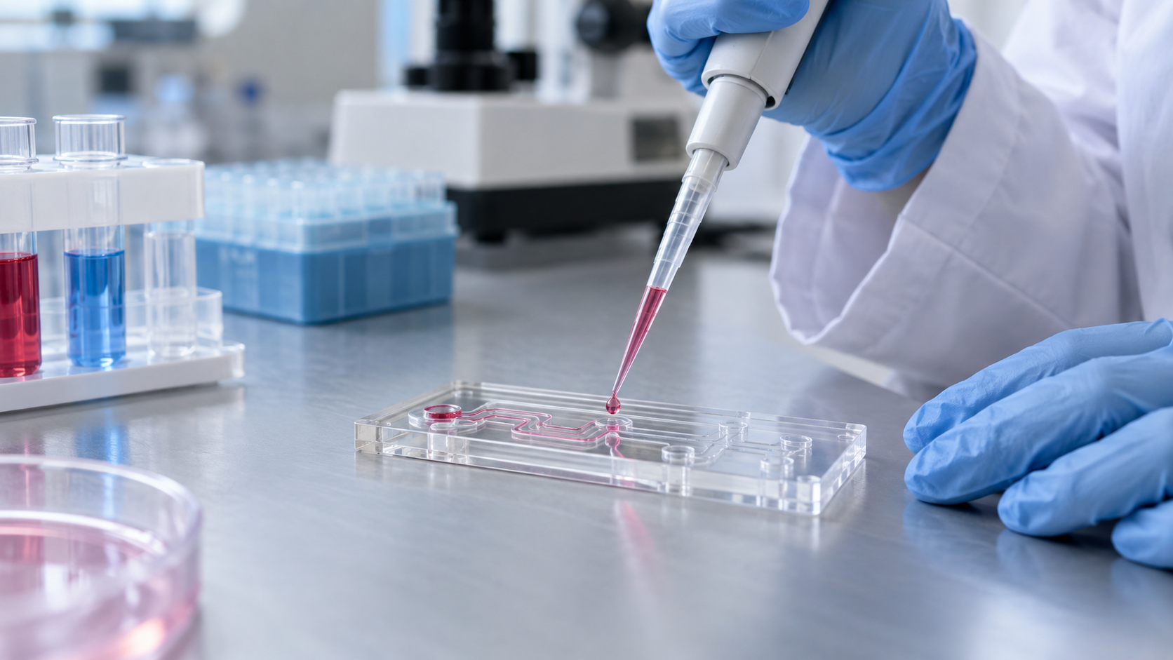
A lab-on-a-chip (LOC) puts the steps of a test onto a small chip with channels tens of micrometers across. A sample goes in, flows by capillary force or by instrument force, reacts and is detected. In the laboratory such chips are often prototyped in PDMS, yet few have reached the market as products. Much of the obstacle is a matter of materials: the material, the molding, the surface, the bonding and the storage of reagents. This article walks through PDMS, COC/COP, PMMA, paper, glass and silicon, manufacturing methods such as injection molding, hot embossing and photolithography, surface treatment, chip bonding, reagent storage and the difficulties of volume manufacture, drawing on peer-reviewed papers and on FDA decision summaries for cartridges that were actually reviewed.
- What a lab-on-a-chip is (the short version)
- What is inside real cartridges: two FDA-reviewed examples
- Materials: PDMS, COC/COP, PMMA, paper, glass and silicon
- A materials engineer's view 1: PDMS is a universal prototyping material, not a material for volume manufacture
- Manufacturing: soft lithography, injection molding, hot embossing and 3D printing
- Surface treatment: making channels wet and making them non-adsorbing
- Bonding and sealing: how firmly a chip is closed
- A materials engineer's view 2: sealing a chip is an adhesion-testing problem
- Storing and releasing reagents
- Challenges of volume manufacture: why commercialization is hard
- Our calculation: bond-strength conversions, flow time and volume ratio
- A materials engineer's view 3: storage stability is the aging of materials and surfaces
- Open issues and what could not be confirmed / Glossary / References / Claim-to-source audit
Sourced = a statement in published material (link given)
Our calculation = a figure this article derived, with the assumptions spelled out
Not yet confirmed = a plan or target with no confirmed record
Structural readings and materials-design interpretations are marked separately as Commentary.
It explains the materials, manufacture and evaluation of chips. It does not recommend any test or cartridge and does not say how to read a test result. Performance and strength values are given with what was tested, on what material and under what conditions (material, conditions, source), and figures from different papers are never lined up to rank products.
1. What a lab-on-a-chip is (the short version)
Microfluidics is the field that handles fluids in channels with dimensions of tens of micrometers. Whitesides's paper (Nature, 2006) describes it as a new field with the potential to influence subjects from chemical synthesis and biological analysis to optics and information technology, but as still at an early stage, with problems to address such as choosing and focusing on initial applications and developing strategies to complete the cycle of development, including commercialization Sourced. A lab-on-a-chip is a chip with such channels that integrates the steps of a test (our own working definition).
- The gap between promise and reality: the review by Chin, Linder and Sia (2012) says that a large part of the excitement behind microfluidics is in its potential for practical devices, yet surprisingly few lab-on-a-chip technologies have been successfully introduced into the market. It reviews commercialization work and its challenges, and says a balance must be struck between achieving real-world impact with integrated devices and designing novel single microfluidic components Sourced
- The search for a "killer application": Becker's commentary "Hype, hope and hubris: the quest for the killer application in microfluidics" (Lab on a Chip, 2009) discusses, as its title says, the search for the field's first decisive application (we checked the title only) Sourced
- This article's viewpoint: a chip is not finished by channel design alone. What it is made of, how it is molded, what its surfaces are, how it is closed, how reagents are loaded and how many months it is stored decide whether it becomes a product (Commentary)
Most of the difficulty of lab-on-a-chip lies not in fluid mechanics but in materials, surfaces, bonding and storage. PDMS, widely used in research, has problems of volume manufacture, molecular absorption and swelling in solvents, and products use thermoplastics, silicon and paper. And a product must be loaded with reagents and still work after months or years in storage.
2. What is inside real cartridges: two FDA-reviewed examples
FDA 510(k) decision summaries record how chip-type cartridges are actually built and what they carry. Here are two Sourced.
- A. i-STAT CHEM8+ (K183688): according to the decision summary, the single-use cartridge has sensors, a fluid pouch, a sample entry well and closure, fluid channels, a waste chamber, and mechanical features for controlled fluid movement. The sensors are microfabricated thin-film electrodes on a silicon chip, with lead lines inside the cartridge and only contact pads exposed to touch the analyzer's contact pins. The analyzer moves fluid across the sensors and finds concentration from the potential difference of ion-selective electrodes. It takes two to three drops of whole blood and is a prescription device used by trained professionals at the point of care or in the laboratory
- B. Xpert MTB/RIF (K143302): according to the decision summary, the single-use cartridge holds reagents including a lyophilized processing control, filters and washes cells, lyses them with glass beads and an ultrasonic horn, mixes the DNA with dry PCR reagents and moves it to an integrated PCR tube. Once the cartridge is placed in the instrument, sample processing and PCR proceed hands-off, with a result in about two hours. The shelf life is 24 months (reagents and cartridges stored at 2-28 °C), and real-time stability was evaluated at four temperatures at time points up to 36 months
What these two show is that a chip-type cartridge is not "a plate with channels carved in it" but a combination of sensors, liquid reagent pouches, dry reagents, a molded flow path, and the instrument that drives them (Commentary).
3. Materials: PDMS, COC/COP, PMMA, paper, glass and silicon
| Material | What is documented (source) |
|---|---|
| PDMS (polydimethylsiloxane) | Review by Bhattacharjee et al.: the vast majority of microfluidic systems of the last two decades were built in PDMS by soft lithography. PDMS is biocompatible, elastomeric, transparent, gas-permeable, water-impermeable, fairly inexpensive, copyright-free, and rapidly prototyped with high precision using simple procedures. But fabrication takes substantial human labor, devices are hard to disseminate outside research labs, and layered molding limits 3D complexity |
| Weaknesses of PDMS | It absorbs small hydrophobic molecules, which can change solution concentrations (Toepke and Beebe). It swells in organic solvents: water, nitromethane, DMSO and ethylene glycol swell it least, while diisopropylamine, triethylamine, pentane and xylenes swell it most (Lee et al.). Hydrophobic recovery after hydrophilization by oxygen plasma and chemical treatment has been studied (Bodas and Khan-Malek; title only checked) |
| Thermoplastic polymers | Review by Becker and Gärtner: in recent years polymers have assumed the leading role as substrate materials for microfluidic devices, with a broad range of material parameters and surface chemistry. Fabrication methods are hot embossing, injection molding, microthermoforming, casting, photolithography and laser ablation |
| COP (cyclic olefin polymer) | Rivera-De Jesus et al.: COP stands out for its exceptional optical clarity, suiting fluorescence-based biosensing, but bonding without compromising mechanical strength or imaging quality remains a challenge. For COC/COP in general, the review by Nunes et al., "Cyclic olefin polymers: emerging materials for lab-on-a-chip applications" (title only checked) |
| PMMA and COC | Tsao et al.: UV/ozone surface treatment enables low-temperature bonding of PMMA and COC microfluidic substrates, with bond strengths approaching those of native polymer substrates bonded above their glass transition temperatures |
| Paper | Title of Martinez et al. (2007): patterned paper as a platform for inexpensive, low-volume, portable bioassays. Review by Yetisen et al.: dipstick and lateral-flow formats have dominated rapid diagnostics for three decades but lack quantitation, and paper-based microfluidics has emerged as a multiplexable point-of-care platform. It covers fabrication, functionalisation, detection, quantification with phones, and scaling up, commercialisation and regulatory issues |
| Glass and silicon | Iliescu et al.: methods of micropatterning glass and silicon and their limitations, bonding methods and electrical connections are surveyed. The capillary-driven chip of Gervais et al. is a silicon channel sealed with PDMS |
All Sourced (abstracts and titles of each reference). Entries marked "title only checked" are based on the title alone; the full text was not checked.
4. A materials engineer's view 1: PDMS is a universal prototyping material, not a material for volume manufacture
Duffy and colleagues (1998) showed how to make channels in PDMS. A channel network designed in CAD is printed at high resolution on a transparency, used as a mask in photolithography to make a master in positive-relief photoresist, and PDMS is cast against it to make a replica. The replica and a flat PDMS slab are oxidized in an oxygen plasma and, brought into conformal contact, seal tightly and irreversibly. Oxidized PDMS also seals irreversibly to glass, silicon, silicon oxide and oxidized polystyrene, and its channel walls become negatively charged in neutral and basic aqueous solutions so that the channels fill easily with water. The whole procedure takes less than 24 hours Sourced. This speed and simplicity made PDMS the research standard. From a materials standpoint, however, these points become walls for manufacture and measurement (Commentary).
- Much manual work: Bhattacharjee et al. say PDMS devices take substantial human labor and are hard to disseminate outside research labs. Replication and plasma bonding are close to piece-by-piece operations
- Molecular absorption: because it absorbs small hydrophobic molecules, the effective concentration of a solution may change in drug screening or cell culture (Toepke and Beebe). In diagnostics, a target or reagent taken up by the wall could change the measurement
- Swelling in solvents: dimensions change in steps or cleaning that use organic solvents. Swelling in water is small (Lee et al.)
- Aging of the surface: the return of a plasma-hydrophilized surface to hydrophobicity over time has been studied (Bodas and Khan-Malek). The period over which a surface stays "wettable" can limit shelf life
McDonald and Whitesides's review (2002) says channels in PDMS are simple to fabricate and that it can incorporate other materials and structures through encapsulation or sealing (reversible and irreversible) Sourced. This flexibility is ideal for research and a disadvantage for standardized volume production (Commentary). For the chemistry and properties of PDMS itself, see this series' article on silicones.
5. Manufacturing: soft lithography, injection molding, hot embossing and 3D printing
The review by Becker and Gärtner (2008) lists, for polymer microfluidic devices, replication methods (hot embossing, injection molding, microthermoforming, casting) and pattern-defining methods (lithography, laser ablation), discusses academic and industrial considerations for their use, and ends with back-end processing Sourced.
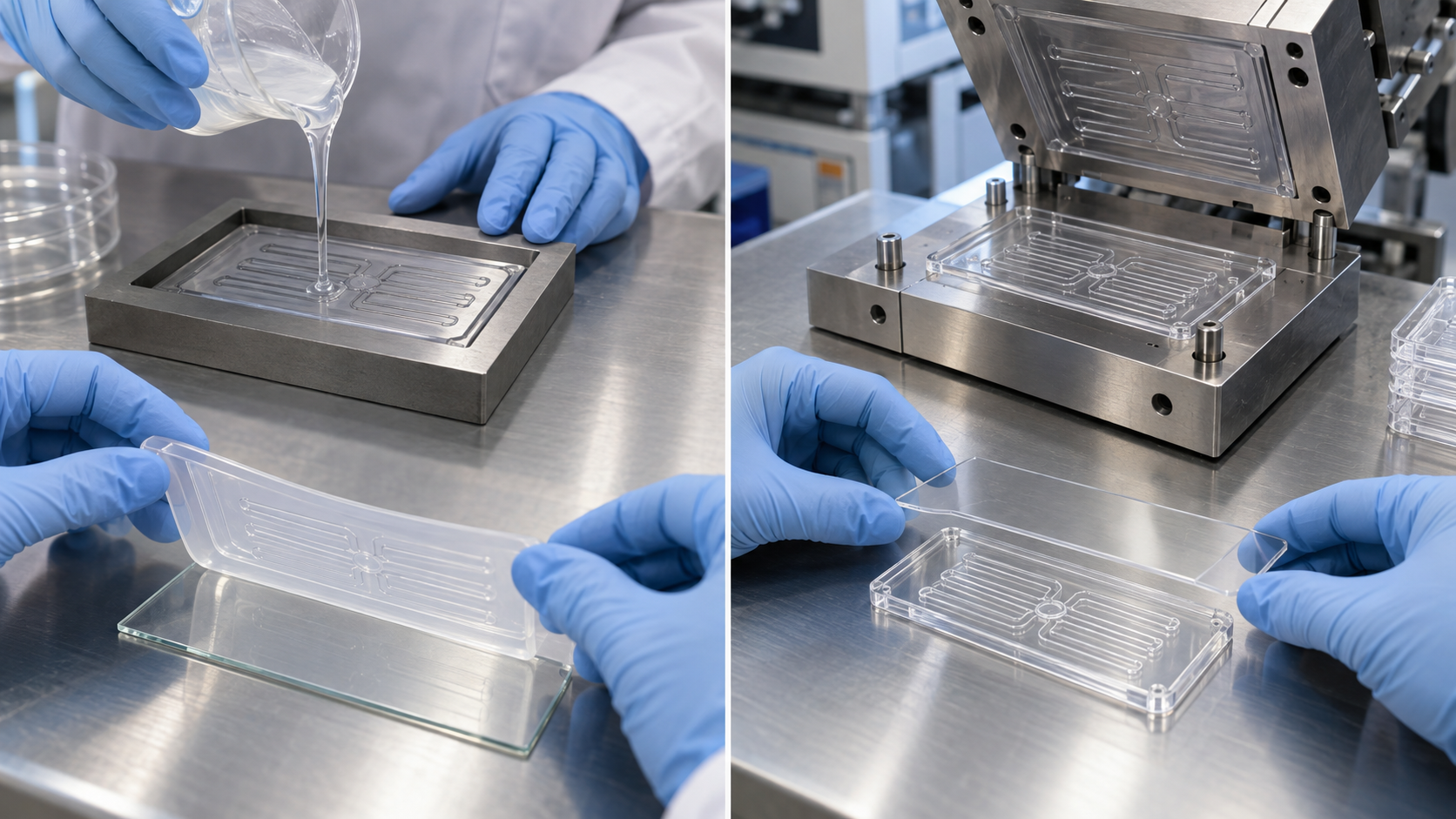
View the original SVG schematic, source notes and numerical details
- PDMS prototyping (soft lithography): as in the previous chapter. The review "Soft lithography" by Xia and Whitesides (1998) is known as the origin of this approach (we checked the title only)
- Injection molding: the review "Micro-injection moulding of polymer microfluidic devices" by Attia et al. (2009) deals with injection molding of polymer devices (title only checked). Injection molding is positioned as a method that can replicate the same shape in large numbers from a mold, hence for volume production (Commentary; we did not confirm the details in primary sources)
- Glass and silicon: Iliescu et al. survey patterning methods for glass and silicon and their limitations, bonding methods and key process parameters, and propose a framework for a complete device fabrication flow Sourced
- 3D printing: the review by Bhattacharjee et al. (2016) says 3D printing has attracted attention for its automated, assembly-free 3D fabrication, rapidly decreasing costs and fast-improving resolution and throughput, but names resolution, throughput and resin biocompatibility as the barriers to adoption, and says resins with properties approaching PDMS are being developed Sourced (a 2016 review; later progress was not checked)
6. Surface treatment: making channels wet and making them non-adsorbing
In microchannels both the force that moves liquid (capillary force) and the loss of sample molecules to the wall (adsorption) are governed by the surface. Surface treatment is at the center of a chip's function. Here are the examples we could confirm Sourced.
| Treatment | Purpose and effect | Source |
|---|---|---|
| Oxygen plasma (PDMS) | Oxidizes PDMS surfaces so they seal tightly and irreversibly. The oxidized walls become negatively charged in neutral and basic aqueous solution, so liquids of high surface energy such as water fill the channels easily | Duffy et al. 1998 |
| Hydrophobic recovery (PDMS) | A study used scanning electron microscopy to investigate the hydrophobic recovery of PDMS after hydrophilization by oxygen plasma and chemical treatment | Bodas and Khan-Malek 2007 (title only checked) |
| Modification of PDMS surfaces | Reviews plasma, graft-polymer coating, dynamic surfactant treatment, hydrosilylation and modification with nanomaterials such as carbon nanotubes and metal nanoparticles. Aims: higher wettability, less non-specific adsorption of hydrophobic species, and display of functional groups for separations and immunoassays | Zhou et al. 2012 (reports from April 2009 to May 2011) |
| UV/ozone (PMMA, COC) | Enables low-temperature bonding. The relationship between UV/ozone exposure and polymer hydrophilicity and surface chemistry (XPS), the stability of treated surfaces after solvent exposure, and the effect on electroosmotic flow in microchannels were evaluated | Tsao et al. 2007 |
| Plasma treatment (COP) | In bonding COP layers, plasma treatment improved bond strength and uniformity across most methods | Rivera-De Jesus et al. 2026 |
All Sourced (abstracts and titles of each reference). Treatment conditions (power, time, atmosphere) and how long the effect lasts could not be confirmed from the abstracts.
Surface treatment affects a chip's performance and shelf life as much as the material does. The next chapters show that surface state matters again in bonding and in reagent storage.
7. Bonding and sealing: how firmly a chip is closed
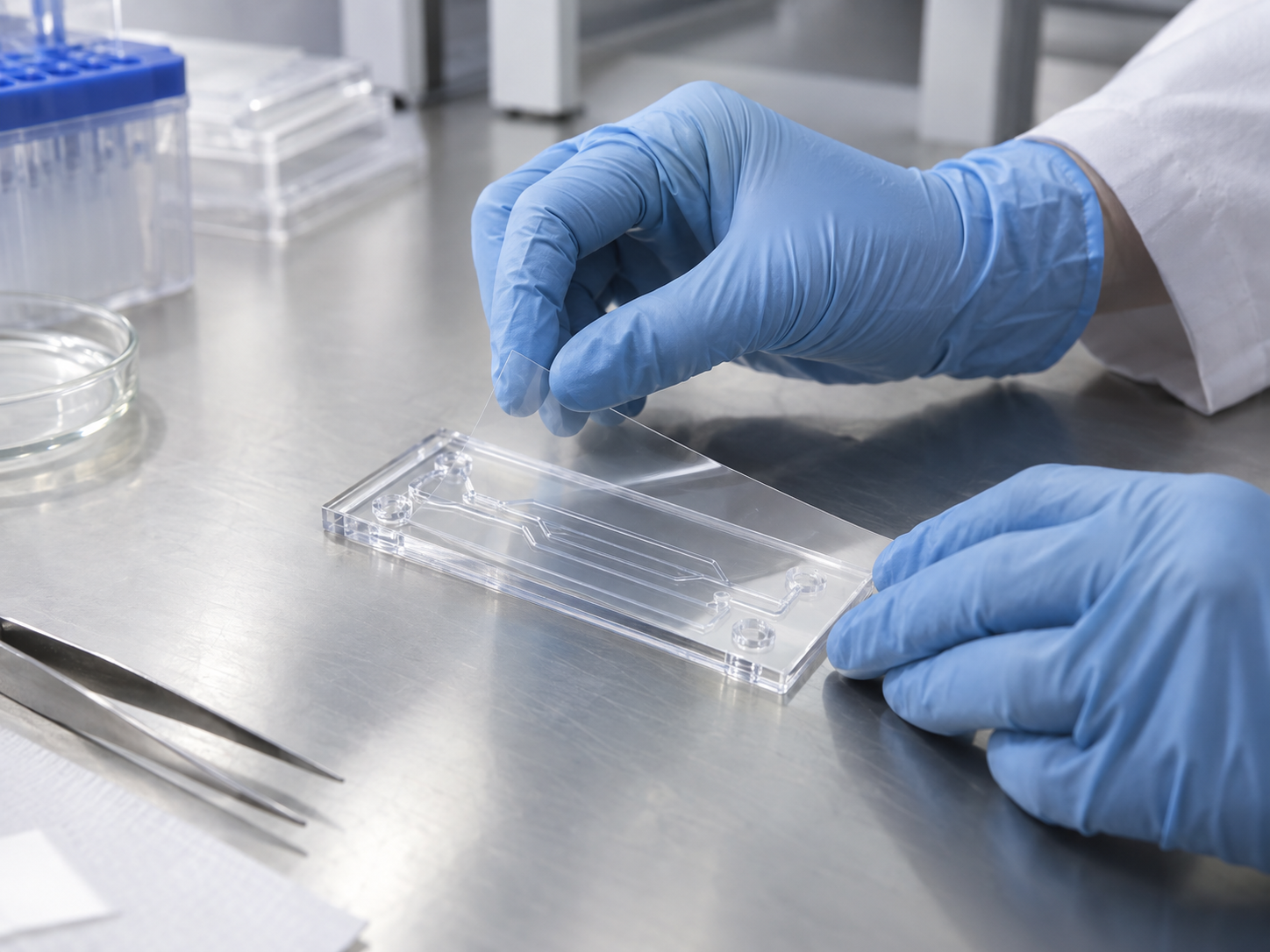
A carved channel becomes a channel only when closed by a lid. If the seal is too weak, liquid leaks, channels collapse and measurements drift. Rivera-De Jesus and colleagues (Biomedical Microdevices, 2026) compared four ways to bond the layers of a COP microfluidic chip using standardized 180-degree peel tests Sourced.
- The four methods: thermal bonding, solvent bonding, UV-curable adhesives and pressure-sensitive adhesives (PSA)
- Results: PSA bonding showed the highest adhesion (0.2-0.8 N/mm), while thermal and solvent bonds were notably weaker (below 0.05 N/mm). The abstract gives no number for UV-curable adhesives. Plasma treatment improved bond strength and uniformity across most methods
- Application: multilayer microfluidic chips were fabricated and assessed for use with particle diffusometry (an optical method that detects Vibrio cholerae DNA through changes in nanoparticle motion), for both mechanical robustness and image intensity suitable for smartphone-based measurement
Other examples include the irreversible bonding of oxidized PDMS (chapter 4), the low-temperature bonding of PMMA and COC by UV/ozone (chapter 6), and the capillary-driven chip of Gervais and colleagues, in which a silicon channel is sealed with a PDMS lid carrying immobilized antibodies Sourced. The last is a design in which the lid is at once the part that closes the chip and the surface where detection happens (Commentary).
8. A materials engineer's view 2: sealing a chip is an adhesion-testing problem
The 180° peel test and "N/mm" (force per width) that Rivera-De Jesus et al. used to evaluate chip bonding are the very tools of adhesion evaluation covered in this series' articles on adhesive strength testing and tapes. Here is the door through which a materials engineer can walk into microfluidic chips (Commentary).
- The pressure-sensitive adhesive layer can become part of the channel wall: PSA bonding was strongest, but the adhesive layer may face the channel. Then questions arise such as whether adhesive components contact the sample or reagents, and whether proteins adsorb (Commentary; we could not confirm from the abstract whether the paper evaluated these)
- Why thermal and solvent bonds are weak: the abstract does not say. A chemically inert surface such as COP may be hard to fuse by melting the interface with solvent or heat (Inference)
- Surface treatment raises strength and uniformity: plasma treatment improved bond strength and uniformity in most methods. This is the same picture as "wetting first, strength later" in the article on adhesives
- Not just strength but optics: as the study assessed image intensity (suitability for smartphone optical measurement), a chip is also an optical component. The thickness, transparency and bubbles of the bonding layer affect the detection signal
- Peel numbers depend on adherend and rate: as the adhesive-strength-testing article showed, peel force depends on specimen, speed and pretreatment, and numbers from different papers cannot be compared directly. The values of Rivera-De Jesus et al. are for that study's conditions
9. Storing and releasing reagents
A diagnostic chip needs its reagents already inside before the sample goes in. The review by Hitzbleck and Delamarche (2013) says microfluidic devices are more complex than test tubes or microtiter plates and that integrating reagents into them is a real challenge, and surveys the many methods of integration and release. Reagents can be in dry or liquid form, integrated directly or linked to carriers, and released by active, passive and hybrid methods Sourced.
- Dried in place: the Xpert MTB/RIF cartridge, after filtering, washing and lysing cells, mixes the DNA with dry PCR reagents and moves it to an integrated PCR tube. In LFAs the labeled antibody is dried together with sugar (such as sucrose), the sugar protecting the structure around the dried particles and dissolving quickly when sample arrives to carry them into the stream (see this series' POCT article) Sourced
- Lyophilized: the Xpert cartridge uses a lyophilized sample processing control (SPC), a control that monitors adequate processing and the presence of PCR inhibitors
- Liquid in a pouch: the i-STAT cartridge has sensors, a fluid pouch, channels and a waste chamber, and the analyzer drives the fluid. The summary says concentration is found from the difference between the electrical signals of the sample and the calibrant solution (the contents of the pouch could not be confirmed from the decision summary)
- Spotted in tiny volume: Gervais and colleagues deposited 10.6 nL of detection antibody solution with an inkjet spotter in a structure beside the flow path of a capillary-driven silicon chip, for release into a flow of 20 µL of serum. Because release is asymmetric, they corrected it with a Dean-flow mixer (nine loops)
Dried and lyophilized reagents have two challenges: stability in storage (enzymes and proteins must not be damaged) and uniform redissolution at use. The "probe check control" in the Xpert decision summary verifies reagent rehydration, PCR tube filling, probe integrity and dye stability Sourced. Confirmation of redissolution is built into the product (Commentary).
10. Challenges of volume manufacture: why commercialization is hard
Why, with so much research, are there so few products on the market? Here are the leads in the primary sources.
| Challenge | Lead in primary sources |
|---|---|
| Few commercial successes | Review by Chin et al.: surprisingly few lab-on-a-chip technologies have reached the market. It organizes the challenges of commercialization, including lessons from experience at Claros Diagnostics. A balance is needed between integrated devices and novel single microfluidic components |
| Choosing applications, completing the cycle | Whitesides: the challenge is to choose and focus on initial applications and to develop strategies to complete the cycle of development, including commercialization |
| Fabrication does not spread beyond the lab | Review by Bhattacharjee et al.: PDMS devices take substantial labor and are hard to disseminate outside research labs. The barriers to 3D printing are resolution, throughput and resin biocompatibility |
| Scale-up and regulation | Review by Yetisen et al. (paper-based): covers challenges to scaling up, commercialisation and regulatory issues, and the factors that limit adoption as real-world products |
| Works together with an instrument | The i-STAT analyzer moves the cartridge's fluid. In Xpert the instrument performs sample processing and PCR. They were reviewed as products that include an instrument, not as chips alone |
| Guaranteeing shelf life | Xpert: 24 months (2-28 °C), with real-time stability evaluated at four temperatures at time points up to 36 months |
All Sourced (abstracts and decision summaries of each reference). The arrangement above is this article's.
The two examples in FDA decision summaries (i-STAT and Xpert) are cases of chip-type cartridges that exist as products under regulation. But both are sold together with a dedicated instrument and are for professional users, and the decision summaries say nothing about manufacturing difficulty, yield or cost (Commentary).
11. Our calculation: bond-strength conversions, flow time and volume ratio
These conversions, from published numbers, are meant to give a sense of scale Our calculation.
- Unit conversion of peel strength: 0.2-0.8 N/mm = 200-800 N/m. Expressed in N/25 mm (× 25) that is 5-20 N/25 mm. The thermal and solvent bonds' "below 0.05 N/mm" is below 1.25 N/25 mm (0.05 × 25).
- Ratio of PSA to thermal/solvent bonding: lower bounds, 0.2 ÷ 0.05 = at least 4 times; upper bounds, 0.8 ÷ 0.05 = at least 16 times ("at least" because the thermal and solvent figures are upper bounds).
- Flow time in a capillary-driven chip: the chip of Gervais et al. analyzes 20 µL of serum over 6 flow paths at 3.3 to 0.46 nL/s. Assuming the sample splits equally among the 6, each path gets 20 ÷ 6 = 3.33 µL = 3,333 nL. At 3.3 nL/s that is 3,333 ÷ 3.3 = about 1,010 s (about 17 minutes); at 0.46 nL/s it is 3,333 ÷ 0.46 = about 7,250 s (about 2 hours). The range of flow rates is 3.3 ÷ 0.46 = about 7.2 times.
- Volume ratio of sample to reagent: against 10.6 nL of detection antibody solution the sample is 20 µL = 20,000 nL. 20,000 ÷ 10.6 = about 1,890 times.
Assumptions and limits: the peel strength is from one paper (COP, 180° peel, under that study's conditions) and cannot be compared directly with values for other materials, adhesives or speeds. The flow-time calculation rests on the simplifying assumptions that the sample splits equally among 6 paths and each path keeps its flow rate; it is not a time reported in the paper. The volume ratio is the ratio of two volumes stated in the paper and does not show reaction stoichiometry.
12. A materials engineer's view 3: storage stability is the aging of materials and surfaces
The Xpert MTB/RIF decision summary derives its 24-month shelf life from real-time stability data at four temperatures (5, 25, 35 and 45 °C) evaluated at time points up to 36 months, using linear regression (from the 24-month point onward the 25 °C condition was changed to 30 °C) Sourced. According to the standards body's page, ISO 23640:2011 covers stability evaluation of in vitro diagnostic reagents, applies to reagents, calibrators, control materials, diluents, buffers and kits, and sets requirements for both real-time and accelerated evaluation Sourced. For a chip, a materials engineer can see that many things can change in storage (Commentary).
- Surface state: a surface made hydrophilic by plasma or UV/ozone can revert over time (hydrophobic recovery of PDMS has been studied). In a chip whose flow depends on wetting, that leads to a change in flow rate, that is, time
- Dry reagents: antibodies protected with sugar and dry PCR reagents deteriorate with moisture and temperature. The barrier properties of the packaging (this series' article on barrier properties and coatings) matter
- Bonded joints: adhesives flow slowly over time (the "slowly flowing solid" of the tape article). Aging of the bonding layer may need to be considered (Inference; not confirmed in the paper's abstract)
- Absorption and leaching: absorption of molecules by PDMS and leaching of additives from plastics matter more the longer the contact time with reagents and sample
A chip's shelf life is thus set not by the shape of the channel but by the combined aging of material, surface, bond, reagent and packaging. A stability-evaluation framework such as ISO 23640 is, for a materials engineer, a tool that bundles these into the single number "shelf life" (Commentary).
13. Open issues and what could not be confirmed
(1) Property values for COC/COP and PMMA could not be confirmed
Values such as water uptake, heat resistance, autofluorescence and solvent resistance could not be confirmed from the abstracts and titles consulted. We limited ourselves to the optical clarity and the bonding challenge of COP (Rivera-De Jesus et al.) and the low-temperature bonding of PMMA and COC (Tsao et al.).
(2) No quantitative figure for PDMS hydrophobic recovery was confirmed
We checked only the title of the paper by Bodas and Khan-Malek. We give no numbers for the rate of recovery or its effect on shelf life.
(3) Yield, cost and mold life in volume manufacture could not be confirmed
We checked only the titles of the injection-molding review by Attia et al. and the COC/COP review by Nunes et al., and did not confirm molding conditions, mold dimensional accuracy or yield. For the review by Chin et al. we do not quote beyond the abstract.
(4) Regulatory classes were confirmed only for two FDA examples
We checked the 510(k) decision summaries for i-STAT and Xpert. We did not check the regulatory treatment of chip-type cartridges in general (EU, Japan) or of research-use-only (RUO) chips.
(5) 3D printing is covered only up to a 2016 review
The review by Bhattacharjee et al. dates from 2016. Later progress in resins and equipment was not checked.
(6) Specific glass and silicon processes were not checked
We kept to the abstract of Iliescu et al. (the survey of patterning, bonding and electrical connections). Specific conditions such as etchants and bonding temperatures were not checked.
- Most of the difficulty of lab-on-a-chip lies in materials, surfaces, bonding and storage. The reviews say surprisingly few technologies have reached the market Sourced
- PDMS is excellent for prototyping but labor-intensive and absorbs molecules. Products use thermoplastics, silicon and the like Sourced
- The strength of a seal can be measured by a 180° peel test. For COP, PSA gave 0.2-0.8 N/mm and thermal and solvent bonds gave below 0.05 N/mm Sourced
- Reagents are loaded on a chip dried, lyophilized, in pouches or spotted. The Xpert cartridge has a 24-month shelf life, with real-time stability data up to 36 months Sourced
- The cartridges that were actually reviewed are sold with dedicated instruments and are for professional users Sourced
14. Glossary
- Microfluidics
- The handling of fluids in channels a few tens of micrometers across.
- Lab-on-a-chip (LOC)
- A small chip with channels that integrates the steps of a test.
- PDMS
- Polydimethylsiloxane. A transparent, gas-permeable elastomer, the standard material for research chips.
- COC / COP
- Cyclic olefin copolymer / polymer. Optically clear thermoplastic polymers.
- Soft lithography
- Replicating by casting PDMS against a mold made by photolithography.
- Hot embossing
- Pressing a mold into heated polymer to transfer the channel shape.
- Injection molding
- Injecting molten polymer into a mold to form a part.
- Hydrophobic recovery
- The tendency of a surface made hydrophilic by plasma or similar treatment to revert to hydrophobic over time.
- Peel test (180°)
- A test that folds back and peels bonded layers at 180°, expressing strength as force per width.
- Pressure-sensitive adhesive (PSA)
- An adhesive that sticks under light finger pressure.
- Lyophilization
- Freeze-drying: freezing and sublimating the water. It keeps proteins and the like stable in storage.
- Capillary-driven
- Moving liquid through channels by capillary force alone, with no pump.
- RUO
- Research Use Only: a category of products not for diagnostic use.
15. References
- Whitesides GM The origins and the future of microfluidics. Nature 442(7101): 368-373 (2006). DOI 10.1038/nature05058 (abstract checked on PubMed, PMID 16871203) — doi.org
- Chin CD, Linder V, Sia SK Commercialization of microfluidic point-of-care diagnostic devices. Lab Chip 12(12): 2118-2134 (2012). DOI 10.1039/c2lc21204h (abstract checked on PubMed, PMID 22344520) — doi.org
- Becker H Hype, hope and hubris: the quest for the killer application in microfluidics. Lab Chip 9(15): 2119-2122 (2009). DOI 10.1039/b911553f (title only checked, PMID 19606286) — doi.org
- Duffy DC, McDonald JC, Schueller OJA, Whitesides GM Rapid prototyping of microfluidic systems in poly(dimethylsiloxane). Anal Chem 70(23): 4974-4984 (1998). DOI 10.1021/ac980656z (abstract checked on PubMed) — doi.org
- McDonald JC, Whitesides GM Poly(dimethylsiloxane) as a material for fabricating microfluidic devices. Acc Chem Res 35(7): 491-499 (2002). DOI 10.1021/ar010110q (abstract checked on PubMed, PMID 12118988) — doi.org
- Toepke MW, Beebe DJ PDMS absorption of small molecules and consequences in microfluidic applications. Lab Chip 6(12): 1484-1486 (2006). DOI 10.1039/b612140c (abstract checked on PubMed, PMID 17203151) — doi.org
- Lee JN, Park C, Whitesides GM Solvent compatibility of poly(dimethylsiloxane)-based microfluidic devices. Anal Chem 75(23): 6544-6554 (2003). DOI 10.1021/ac0346712 (abstract checked on PubMed, PMID 14640726) — doi.org
- Bhattacharjee N et al. The upcoming 3D-printing revolution in microfluidics. Lab Chip 16(10): 1720-1742 (2016). DOI 10.1039/c6lc00163g (abstract checked on PubMed, PMID 27101171) — doi.org
- Becker H, Gärtner C Polymer microfabrication technologies for microfluidic systems. Anal Bioanal Chem 390(1): 89-111 (2008). DOI 10.1007/s00216-007-1692-2 (abstract checked on PubMed, PMID 17989961) — doi.org
- Nunes PS et al. Cyclic olefin polymers: emerging materials for lab-on-a-chip applications. Microfluid Nanofluid 9(2-3): 145-161 (2010). DOI 10.1007/s10404-010-0605-4 (title only checked) — doi.org
- Attia UM, Marson S, Alcock JR Micro-injection moulding of polymer microfluidic devices. Microfluid Nanofluid 7(1): 1-28 (2009). DOI 10.1007/s10404-009-0421-x (title only checked) — doi.org
- Tsao CW et al. Low temperature bonding of PMMA and COC microfluidic substrates using UV/ozone surface treatment. Lab Chip 7(4): 499-505 (2007). DOI 10.1039/b618901f (abstract checked on PubMed, PMID 17389967) — doi.org
- Rivera-De Jesus JA et al. Optical biosensing using particle diffusometry on thermoplastic microfluidic chips bonded using direct and indirect chip bonding methods. Biomed Microdevices 28(2): 29 (2026). DOI 10.1007/s10544-026-00810-4 (CC BY; abstract checked on Europe PMC, PMID 42008229) — doi.org
- Zhou J, Ellis AV, Voelcker NH Surface modification for PDMS-based microfluidic devices. Electrophoresis 33(1): 89-104 (2012). DOI 10.1002/elps.201100482 (abstract checked on PubMed, PMID 22128067) — doi.org
- Bodas D, Khan-Malek C Hydrophilization and hydrophobic recovery of PDMS by oxygen plasma and chemical treatment — An SEM investigation. Sens Actuators B Chem 123(1): 368-373 (2007). DOI 10.1016/j.snb.2006.08.037 (title only checked) — doi.org
- Iliescu C et al. A practical guide for the fabrication of microfluidic devices using glass and silicon. Biomicrofluidics 6(1): 016505 (2012). DOI 10.1063/1.3689939 (abstract checked on PubMed, PMID 22662101) — doi.org
- Gervais L, de Rooij N, Delamarche E Microfluidic chips for point-of-care immunodiagnostics. Adv Mater 23(24): H151-H176 (2011). DOI 10.1002/adma.201100464 (abstract checked on PubMed, PMID 21567479) — doi.org
- Gervais L, Hitzbleck M, Delamarche E Capillary-driven multiparametric microfluidic chips for one-step immunoassays. Biosens Bioelectron 27(1): 64-70 (2011). DOI 10.1016/j.bios.2011.06.016 (abstract checked on PubMed, PMID 21752632) — doi.org
- Hitzbleck M, Delamarche E Reagents in microfluidics: an 'in' and 'out' challenge. Chem Soc Rev 42(21): 8494-8516 (2013). DOI 10.1039/c3cs60118h (abstract checked on PubMed, PMID 23925517) — doi.org
- Yetisen AK, Akram MS, Lowe CR Paper-based microfluidic point-of-care diagnostic devices. Lab Chip 13(12): 2210-2251 (2013). DOI 10.1039/c3lc50169h (abstract checked on PubMed, PMID 23652632) — doi.org
- Martinez AW et al. Patterned paper as a platform for inexpensive, low-volume, portable bioassays. Angew Chem Int Ed 46(8): 1318-1320 (2007). DOI 10.1002/anie.200603817 (title only checked, PMID 17211899) — doi.org
- U.S. Food and Drug Administration (FDA) 510(k) decision summary K183688, i-STAT CHEM8+ cartridge with the i-STAT 1 System (Abbott Point of Care) — accessdata.fda.gov
- FDA 510(k) decision summary K143302, Xpert MTB/RIF (Cepheid) — accessdata.fda.gov
- Koczula KM, Gallotta A Lateral flow assays. Essays Biochem 60(1): 111-120 (2016). DOI 10.1042/EBC20150012 (open access, PMC4986465) — doi.org
- EVS (Estonian Centre for Standardisation and Accreditation) ISO 23640:2011 In vitro diagnostic medical devices — Evaluation of stability of in vitro diagnostic reagents — evs.ee
- Xia Y, Whitesides GM Soft lithography. Annu Rev Mater Sci 28: 153-184 (1998). DOI 10.1146/annurev.matsci.28.1.153 (title only checked) — doi.org
16. Claim-to-source audit
| Claim in the text | Basis | Type |
|---|---|---|
| The definition of microfluidics (fluids in channels tens of micrometers across), the field at an early stage, and the challenges of choosing initial applications and completing the cycle through commercialization | Abstract of Whitesides (2006) Reference 1 https://doi.org/10.1038/nature05058 | Sourced |
| Surprisingly few lab-on-a-chip technologies have reached the market. The review of commercialization challenges. The balance between integrated devices and single components | Abstract of Chin et al. (2012) Reference 2 https://doi.org/10.1039/c2lc21204h | Sourced |
| The title of Becker's commentary | Title of Becker (2009) Reference 3 https://doi.org/10.1039/b911553f | Sourced |
| The rapid-prototyping procedure for PDMS channels (CAD, transparency mask, photolithographic master, PDMS replica, oxygen plasma, irreversible sealing, sealing to glass and silicon, negatively charged walls, filling with water, within 24 hours) | Abstract of Duffy et al. (1998) Reference 4 https://doi.org/10.1021/ac980656z | Sourced |
| Channels in PDMS are simple to fabricate and can incorporate other materials and structures by encapsulation or sealing | Abstract of McDonald and Whitesides (2002) Reference 5 https://doi.org/10.1021/ar010110q | Sourced |
| PDMS absorbs small hydrophobic molecules and can change solution concentrations | Abstract of Toepke and Beebe (2006) Reference 6 https://doi.org/10.1039/b612140c | Sourced |
| Swelling of PDMS in solvents (water, nitromethane, DMSO, ethylene glycol least; diisopropylamine, triethylamine, pentane, xylenes most) | Abstract of Lee et al. (2003) Reference 7 https://doi.org/10.1021/ac0346712 | Sourced |
| The advantages of PDMS (biocompatible, elastomeric, transparent, gas-permeable, water-impermeable, inexpensive, copyright-free, rapid prototyping) and its drawbacks (labor, hard to disseminate, 3D limits). The barriers to 3D printing (resolution, throughput, resin biocompatibility) | Abstract of Bhattacharjee et al. (2016) Reference 8 https://doi.org/10.1039/c6lc00163g | Sourced |
| Polymers as the leading substrate materials; replication methods (hot embossing, injection molding, microthermoforming, casting) and pattern-defining methods (lithography, laser ablation); back-end processing | Abstract of Becker and Gärtner (2008) Reference 9 https://doi.org/10.1007/s00216-007-1692-2 | Sourced |
| The titles of the COC/COP review, the injection molding review, "Soft lithography" and the study of PDMS hydrophobic recovery | Titles of each paper (checked on Crossref) Reference 10 https://doi.org/10.1007/s10404-010-0605-4, Reference 11 https://doi.org/10.1007/s10404-009-0421-x, Reference 15 https://doi.org/10.1016/j.snb.2006.08.037, Reference 26 https://doi.org/10.1146/annurev.matsci.28.1.153 | Sourced |
| Low-temperature bonding of PMMA and COC by UV/ozone; the relation of UV/ozone exposure to hydrophilicity and surface chemistry; stability after solvent exposure; electroosmotic flow | Abstract of Tsao et al. (2007) Reference 12 https://doi.org/10.1039/b618901f | Sourced |
| The optical clarity of COP and its bonding challenge. The 180° peel results for four bonding methods (PSA 0.2-0.8 N/mm; thermal and solvent below 0.05 N/mm), the effect of plasma treatment, the application to particle diffusometry | Abstract of Rivera-De Jesus et al. (2026) Reference 13 https://doi.org/10.1007/s10544-026-00810-4 | Sourced |
| Methods of PDMS surface modification (plasma, graft polymer, dynamic surfactant, hydrosilylation, nanomaterials) and their aims (wettability, suppression of non-specific adsorption, functional groups) | Abstract of Zhou et al. (2012) Reference 14 https://doi.org/10.1002/elps.201100482 | Sourced |
| Patterning methods, bonding methods and electrical connections for glass and silicon | Abstract of Iliescu et al. (2012) Reference 16 https://doi.org/10.1063/1.3689939 | Sourced |
| An overview of microfluidic chips for point-of-care immunodiagnostics (materials, surface treatment, sample processing, elements) | Abstract of Gervais et al. (2011, Adv Mater) Reference 17 https://doi.org/10.1002/adma.201100464 | Sourced |
| A capillary-driven chip: silicon channel sealed with a PDMS lid, 20 µL of serum, six flow paths, flow rates 3.3 to 0.46 nL/s, 10.6 nL of antibody solution inkjet-spotted, a Dean-flow mixer | Abstract of Gervais et al. (2011, Biosens Bioelectron) Reference 18 https://doi.org/10.1016/j.bios.2011.06.016 | Sourced |
| Methods of integrating and releasing reagents (dry and liquid, direct and carrier-linked, active, passive and hybrid) | Abstract of Hitzbleck and Delamarche (2013) Reference 19 https://doi.org/10.1039/c3cs60118h | Sourced |
| Paper-based microfluidics (limits of dipstick and lateral flow, fabrication, functionalisation, detection, quantification, scale-up, commercialisation, regulation) | Abstract of Yetisen et al. (2013) Reference 20 https://doi.org/10.1039/c3lc50169h | Sourced |
| The title of the patterned-paper bioassay paper | Title of Martinez et al. (2007) Reference 21 https://doi.org/10.1002/anie.200603817 | Sourced |
| The make-up of the i-STAT CHEM8+ cartridge (sensors, fluid pouch, sample entry, channels, waste chamber, mechanical features), thin-film electrodes, the analyzer moving the fluid, potentiometric measurement, 2-3 drops of whole blood, a prescription device for trained users | FDA 510(k) decision summary K183688 Reference 22 https://www.accessdata.fda.gov/cdrh_docs/reviews/K183688.pdf | Sourced |
| The make-up of the Xpert MTB/RIF cartridge (lyophilized processing control, filtering, washing and lysis, glass beads and ultrasonic horn, dry PCR reagents, integrated PCR tube, probe check control), a result in about 2 hours, 24-month shelf life (2-28 °C), real-time stability at four temperatures up to 36 months | FDA 510(k) decision summary K143302 Reference 23 https://www.accessdata.fda.gov/cdrh_docs/reviews/K143302.pdf | Sourced |
| In an LFA's conjugate pad the labeled antibody is dried with sugar; the sugar protects the structure and dissolves quickly with sample | Koczula and Gallotta (2016, open access) Reference 24 https://doi.org/10.1042/EBC20150012 | Sourced |
| Title and scope of ISO 23640:2011 (stability of reagents, calibrators, control materials, buffers and kits; real-time and accelerated) | EVS standard page Reference 25 https://www.evs.ee/en/iso-23640-2011 | Sourced |
| Unit conversion of peel strength (0.2-0.8 N/mm = 5-20 N/25 mm; below 0.05 N/mm = below 1.25 N/25 mm), the PSA to thermal/solvent ratio (at least 4 to 16 times), flow time in a capillary-driven chip (about 17 minutes to about 2 hours; about 7.2 times), the sample-to-reagent volume ratio (about 1,890 times) | Our calculation. Assumptions: peel strengths are the values in the abstract of Rivera-De Jesus et al.; the flow time assumes the sample splits equally among six paths, each at a constant rate; the volumes are those in the abstract of Gervais et al. | Our calculation |
| The reading that a chip-type cartridge is a combination of sensors, pouches, dry reagents, flow path and instrument. The reading that PDMS's advantages become walls for manufacture and measurement. Injection molding as suited to volume production. The point that a PSA layer can face the channel. Why thermal and solvent bonds are weak (inference). Aging of the bonding layer (inference). The link to the adhesive-strength-testing article. Shelf life as the sum of aging of material, surface, bond, reagent and packaging | Commentary by this article, built on the sourced facts above (inferences are marked in the text) | Commentary |
| Property values of COC/COP and PMMA, a quantitative figure for PDMS hydrophobic recovery, yield, cost and mold life in volume manufacture, regulation in the EU and Japan and the handling of RUO chips, progress in 3D printing after 2016, specific process conditions for glass and silicon | Could not be confirmed in the public sources consulted for this article, and so are not stated | Commentary |
| That Figs. 1 to 3 and 5 to 7 are explanatory drawings, and that the hero image and Fig. 4 are AI-generated images that do not show real products, chips or production equipment | Note by this article | Commentary |
Last updated 4 October 2026. Sources are limited to primary material (peer-reviewed papers, FDA 510(k) decision summaries and the official page of a standards body). Because the article includes structural readings and materials-design interpretations, those are marked as Commentary and kept separate from sourced fact. Property values of COC/COP and PMMA, a quantitative figure for PDMS hydrophobic recovery, yield, cost and mold life in volume manufacture, regulation in the EU and Japan, and progress in 3D printing after 2016 are not stated, because no published primary source could be confirmed. All figures are explanatory concept graphics. Figs. 1 to 3 and 5 to 7 are vector drawings; the hero image and Fig. 4 are AI-generated images, and none of them shows a real product, chip or production equipment. This article explains materials, manufacture and evaluation and is not medical advice.