TECHNOLOGY EXPLAINER
Nanocoatings and Thin Films
— not “how thin is it?” but “where is it missing?”
Anti-reflection, water repellency, barrier and hard coatings: films a few nanometers to a few hundred nanometers thick do real work on glass, lenses, films and tools. Yet the word “nanocoating” means different things depending on whether the thickness is nanoscale or the internal structure is. This explainer draws on ISO terminology standards, test standards, manufacturers' technical data and public documents from the EU, Japan and the US to lay out a map of deposition methods, what the films do, how they are evaluated (thickness, adhesion, pinholes), and the environmental rules around PFAS-type water repellents. It does not rank products or companies, and it is not legal advice.
- What a nanocoating is: the short version
- A map of deposition methods: physical and chemical, dry and wet
- Our calculation: how dip coating gets to a nanometer-scale thickness
- A materials engineer's view (1): films carry stress
- Anti-reflection: erasing light with thin-film interference
- Water and oil repellency: how to read manufacturers' stated values
- Barrier and hard coatings: defects and thickness
- Evaluation: thickness, adhesion, pinholes
- A materials engineer's view (2): the same film gives different numbers with different methods
- Environmental rules, centered on PFAS-type water repellents
- What is still hard, and what could not be confirmed
- Glossary / References / Claim-to-source audit
Sourced = stated in published material (link given)
Our calculation = a figure this article derived, with the assumptions spelled out
Not yet confirmed = a plan, target or matter under deliberation with no confirmed outcome
Structural readings and materials-design interpretations are marked separately as Commentary, and weakly supported ideas as Inference.
Company figures are manufacturers' stated (typical) values, and numbers measured under different conditions are not ranked. Regulations are described by stage (proposed, adopted, applying) and were checked on 9 October 2026.
This is an explainer of technology and rules. It is not advice on choosing a product, on legal compliance, or on safety and health. It also does not say that nano-sized things are inherently safe or hazardous. Rules change, so check the original text and the current position before relying on it.
1. What a nanocoating is: the short version
In the standards, “nanocoating” has two senses. The introduction to ISO/TS 80004-11:2017 sorts films into two groups Sourced.
- Films whose thickness is nanoscale: nanolayer, nanocoating and nanofilm. In ISO's scheme these are classed as nano-objects
- Films whose internal or surface structure is nanoscale: nanostructured layers, coatings and films (nanocomposites, films with dispersed nano-objects and so on), classed as nanostructured materials
- Loose usage: the same introduction says the words film, coating and layer are often used synonymously, and that nearly all PVD and CVD coatings are nanostructured
ISO/TS 80004-11 was withdrawn in 2023, and the same grouping now sits in ISO 80004-1:2023, the core vocabulary standard for nanotechnology, in clause 3.7 on terms for nanocoatings, nanolayers, nanofilms and related terms Sourced. The introduction to ISO 80004-1 says the lower limit of the nanoscale is approximately 1 nm, that the definition of “nanoscale” in the ISO 80004 series is a general descriptor to aid communication, and that articles made to contain nanomaterials are not necessarily nanomaterials themselves Sourced. (The definitions are paywalled; we checked the public contents and introduction. The nanoscale is generally taken as roughly 1 to 100 nm.)
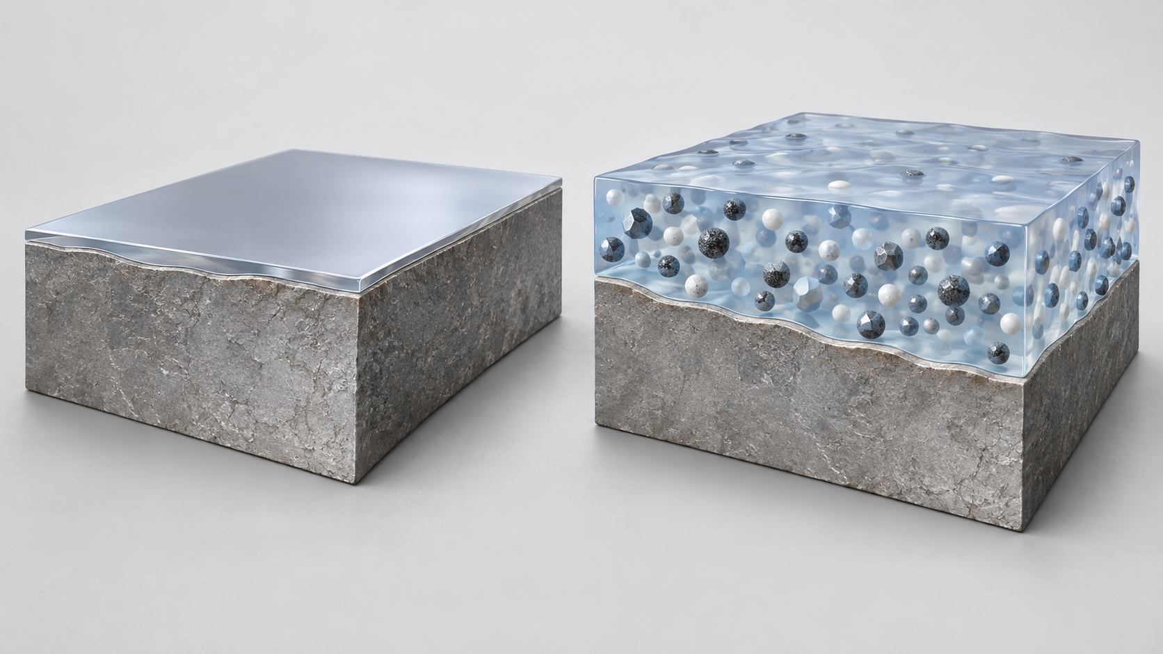
Shapes, colors and dimensions are illustrative. Consult the original schematic below for exact values and label correspondence.
View the original SVG schematic and exact annotations
Reading guide and original schematic labels: Two senses of "nanocoating" (conceptual diagram based on ISO's grouping) / Schematic film cross-sections; not real micrographs or dimensions. / 1. The thickness is nanoscale / 2. The internal structure is nanoscale / Film thickness (an external dimension) of about 1 to 100 nm / Examples: anti-reflection films, very thin repellent films / Terms: nanolayer / nanocoating / nanofilm / The film may be thick, but has nanoscale structure inside / Examples: nanoparticle dispersions, nanocomposites, multilayers / Terms: nanostructured coating and so on / The grouping follows the introductions to ISO/TS 80004-11:2017 [Ref. 2] and ISO 80004-1:2023 [Ref. 1].
The standard itself accepts that “nanocoating” in a catalogue or datasheet may refer to thickness or to structure. Its introduction gives the example of multilayer coatings that protect surfaces from wear, in which individual layers are only a few nanometers thick Sourced. That is sense 2: micrometers overall, nano inside. An anti-reflection film about a hundred nanometers thick overall is sense 1. When reading a specification, first find out whether it refers to total thickness, layer structure and individual layer thicknesses, or internal structure (grains, particles, voids) (our commentary).
2. A map of deposition methods: physical and chemical, dry and wet
There are many ways to make a nanometer-scale film. The introduction to ISO/TS 80004-11 lists as deposition techniques whose terms are in use coating, electrochemical deposition (ECD), spin coating, PVD (physical vapour deposition), CVD (chemical vapour deposition), sol-gel deposition, ALD (atomic layer deposition), LBL (layer-by-layer deposition) and Langmuir-Blodgett deposition Sourced. ISO/TS 80004-8:2020, the vocabulary for nanomanufacturing processes, likewise gives deposition processes, etching processes, and printing and coating their own clauses Sourced. In his historical review of sputter deposition (2017), Greene writes that sputtering was first reported in the early 1800s and already dominated the optical-coating market by 1880, and that roll-to-roll coating dates from the mid-1930s Sourced.
| Method | How the film forms | What it is good at | Watch out for |
|---|---|---|---|
| Evaporation (vacuum evaporation) | Material evaporated by heating condenses on the substrate | Optical and metal films; deposition can be stopped while monitoring thickness | Travels in straight lines, so sidewalls of steps coat poorly. Arriving species have low energy, so films can be loose |
| Sputtering | Ions in a plasma knock atoms off a target and they land on the substrate | Keeps alloy and compound composition well; adhesion is relatively good; large-area use is established | The substrate is exposed to plasma and energetic particles. Film stress changes strongly with conditions |
| CVD | A precursor gas reacts on the substrate to form a solid film | Can coat complex shapes (depending on conditions). Insulating films, DLC and so on | Reaction temperature and by-products. Handling of precursor gases |
| Sol-gel / dip / spin | A precursor solution is applied, then dried and fired to an oxide film | No vacuum tool needed and low cost. Can coat large or curved substrates | Shrinks on drying and firing, so cracks are likely. Thickness is set by withdrawal speed, viscosity and solids content |
This table is our commentary on the general character of each method, not performance figures for particular tools, materials or conditions. For the history of sputtering see Greene's review [Reference 4]; for CVD see Choy (2003) [Reference 5].
3. Our calculation: how dip coating gets to a nanometer-scale thickness
Sol-gel dip coating simply dips a substrate in a solution and withdraws it at a constant speed. As covered in Brinker et al., “Fundamentals of sol-gel dip coating” (1991), the wet film left just after withdrawal is set by withdrawal speed and the liquid's viscosity, surface tension and density. A standard approximation when the capillary number (the ratio of viscous to surface-tension forces) is small is the Landau-Levich relation (our commentary; we did not check the equation in the paper itself).
We assume the following conditions ourselves Our calculation.
- Equation: h = 0.94 (ηU)2/3 / (γ1/6 (ρg)1/2) (h: wet film thickness; η: viscosity; U: withdrawal speed; γ: surface tension; ρ: density; g: gravitational acceleration)
- Assumptions: η = 2 mPa·s, γ = 22 mN/m, ρ = 800 kg/m³ (an ethanol-based liquid), U = 1 mm/s
- Calculation: (0.002 × 0.001)2/3 = 1.58×10⁻⁴, γ1/6 = 0.529 and (800 × 9.81)1/2 = 88.6, so h = 0.94 × 1.58×10−4 / (0.529 × 88.6) = about 3.2 µm
- After drying: if the solids (the part that becomes oxide) are 1 vol% of the liquid, 3.2 µm × 0.01 = about 32 nm (volume change from shrinkage and firing ignored)
- Capillary number: ηU/γ = 0.002 × 0.001 / 0.022 = 9×10⁻⁵, within the “small” range where the relation holds
Assumptions and limits: viscosity, surface tension and solids content are all assumptions of this article and not values for a real sol. In practice solvent evaporates during withdrawal and the liquid's composition changes, so this equation does not fix the real thickness. The point is the order of magnitude: a wet film of a few micrometers becomes a nanometer-scale film after drying if solids are 1%.
Because wet thickness changes only gently with speed (power 2/3), the calculation suggests it is more effective to tune thickness by solids content (dilution) than by withdrawal speed (our commentary). Halve the solids and the dry thickness halves; halve the speed and the wet film only drops to about 0.63 times. On the other hand, the lower the solids, the more likely the film is to fail to spread evenly and break into islands during drying and firing. That is an inference; the official material used here does not confirm it.
4. A materials engineer's view (1): films carry stress
A deposited film holds internal stress, from thermal-expansion mismatch with the substrate, bombardment by depositing particles, volume change on crystallisation and so on. Stress bends the substrate. In 1909 Stoney wrote down the bending of a substrate caused by the tension of a deposited metal film Sourced (Stoney, Proc. R. Soc. A 82, 172).
Using Stoney's relation (R = Ms hs² / (6 σ hf)) and conditions we assume, we estimate the size of the bow Our calculation.
- Assumptions: film thickness hf = 100 nm; film stress σ = 1 GPa; a silicon wafer 100 mm in diameter and hs = 0.5 mm thick; biaxial modulus of the substrate Ms = 180 GPa (a value we set)
- Radius of curvature: R = 180×109 × (0.5×10−3)² / (6 × 109 × 100×10−9) = 45,000 / 600 = 75 m
- Bow over a 100 mm diameter (height difference between center and edge): d²/(8R) = (0.1)² / (8 × 75) = about 17 µm
- Force the film exerts per unit width: σ × hf = 109 × 100×10−9 = 100 N/m
Assumptions and limits: 1 GPa is a film stress we assumed; real sign and size change with conditions and materials. Stoney's relation is an approximation for films much thinner than the substrate and small bows.
Even a 100 nm film, if it carries 1 GPa, puts 100 N/m of force per unit width on the substrate. Thin does not mean mechanically negligible (our commentary). The bow is inversely proportional to the square of substrate thickness, so thinner substrates (films, thinned wafers, thin glass) bow more under the same film. Optical coatings are sometimes designed to balance the stress of a multilayer by combining compressive and tensile layers, but the official material used here did not confirm specific methods.
5. Anti-reflection: erasing light with thin-film interference
An uncoated glass surface reflects about 4% of light at each interface, so two surfaces pass only about 92%, as an Edmund Optics technical article explains Sourced. An anti-reflection film sets its optical thickness to an odd number of quarter wavelengths so that the light reflected from the film surface and from the film-glass interface cancel by a half-wavelength shift Sourced. The company gives a λ/4 layer of MgF2 centered at 550 nm (refractive index 1.38 at 550 nm) as the simplest anti-reflection coating, and says results vary with the type of glass Sourced (the manufacturer's own statement).
We calculate under idealised conditions that ignore the wavelength dependence of refractive index Our calculation.
- Assumptions: glass index ns = 1.52 (our assumption); MgF2 n = 1.38 (as stated by Edmund Optics); air n0 = 1; normal incidence; no absorption or scattering; design wavelength 550 nm
- Thickness: d = λ / (4n) = 550 / (4 × 1.38) = about 99.6 nm
- Uncoated glass: R = ((ns − 1) / (ns + 1))² = (0.52 / 2.52)² = about 4.26%
- Single MgF2 layer (λ/4): R = ((n² − ns) / (n² + ns))² = (0.3844 / 3.4244)² = about 1.26%
- Why it does not reach zero: the ideal index for a single layer is √(n0 ns) = √1.52 = about 1.23, and MgF2 (1.38) is higher
- Tolerance: if thickness is off by 10%, reflectance at 550 nm goes from about 1.26% to about 1.34%. At 400 nm it is about 2.2% and at 700 nm about 1.6% (in this idealised model)
Assumptions and limits: this ignores dispersion of the refractive index, the type of substrate, angle of incidence and film porosity. It will not match the measured spectra manufacturers publish. It is meant to show the trend.
| What was published | Source and conditions |
|---|---|
| Single-layer MgF2 anti-reflection: R < 1.5% (540 nm), R < 2% (400 to 700 nm). The same page also lists rows of R < 2.0% (540 nm) and R < 3.0% (400 to 700 nm); the difference between the two rows could not be confirmed on the page | CASTECH coating specification page. Manufacturer's stated values [Reference 9] |
| Multilayer visible-range coating (VIS 0°): average reflectance 0.4% over 425 to 675 nm (0° incidence) | Edmund Optics technical article, in its description of coating options [Reference 8] |
| Nanostructure can also suppress reflection: a paper on reducing lens reflection by the “moth eye” principle | Clapham and Hutley, Nature 244, 281 (1973). Only title and bibliographic details checked [Reference 11] |
All Sourced (manufacturers' statements; a paper's title). Wavelength range, substrate, angle and the way of averaging differ, so the values cannot be ranked against each other. For a review of anti-reflective coatings see Raut et al. (2011) [Reference 10].
There is generally no dense material with the ideal index (about 1.23). Three routes follow: multilayers (Edmund Optics' VIS 0° averages 0.4%), lower-index porous films, and texturing the surface itself (the moth eye) (our commentary). Porous films lower the index, but mechanical strength, soiling and moisture uptake are likely weak points. That is an inference; we did not confirm it in the official material used here. An anti-reflection film sits at the outermost surface, so resistance to fingerprints and scuffing becomes part of its performance. Our inference is that this is why the repellent films of the next section are layered on top.
6. Water and oil repellency: how to read manufacturers' stated values
The performance of a repellent film is not settled by the water contact angle alone. The sliding angle, the values for oil, and the values after rubbing all matter. The technical datasheet for Daikin's OPTOOL DSX-F (August 2026 edition) describes a fluorine-based anti-smudge coating and gives the values below Sourced. The datasheet notes that these are representative values for an example deposited on glass by PVD, and are not guaranteed (manufacturer's stated values).
| Item | DSX-F | DSX-E | Conditions and notes |
|---|---|---|---|
| Water contact angle | 115° | 114° | Representative value for an example deposited on glass by PVD |
| Water sliding angle | 16° | 17° | Same |
| n-Hexadecane contact angle / sliding angle | 66° / 4° | 67° / 3° | Values for an oil |
| Water contact angle after abrasion | 109° | 108° | 2000 SW abrasions (as written; SW is not defined in the datasheet), contact area 1 cm², load 1 kgf |
| Coefficient of friction | 0.07 | 0.07 | OA paper as the friction element, speed 200 mm/min, load 200 gf |
| Haze | < 0.20 | < 0.20 | Unit and method not stated in the datasheet |
All Sourced (Daikin OPTOOL DSX-F datasheet [Reference 13]; manufacturer's stated, typical values). The datasheet says the coating forms a nanometer-scale thin film and does not affect optical properties, but gives no film-thickness figure and no detailed composition. The solvent is hydrofluoroether and the active-ingredient concentration is 19.0 to 21.0 mass%.
The datasheet table sets side by side the initial contact angle (115°), the angle after abrasion (109°), the sliding angle (16°), the oil contact angle (66°) and the friction coefficient. Going from 115° to 109° is a drop of 6° (about 5%) Our calculation ((115 − 109) / 115 = 0.052). The datasheet does not say how its abrasion test (SW, 1 cm², 1 kgf, 2000 cycles) maps onto rubbing in real use. In judging a repellent film, first confirm under what condition, and after how many rubs, a value was obtained (our commentary).
Contact-angle measurement has a standard too. ASTM D7334 is a practice for measuring surface wettability by advancing contact angle, and warns that the contact angle cannot give a surface-tension value directly Sourced. The introduction to ISO 80004-1:2023 says that surfaces intentionally modified or textured to have nanoscale heterogeneity qualify a material as nanostructured, while ordinary surfaces do not Sourced. Quéré's review (2008) treats the relation between surface roughness and wetting [Reference 12].
7. Barrier and hard coatings: defects and thickness
(1) Barrier: a nanometer-thick film is governed by its defect area
For thin inorganic films that block gases and water vapour, performance can be set by the number and size of defects (pinholes) rather than by the density of the film itself. The series explainers on barrier properties and coatings (polymers and resins) and on encapsulation and barrier layers (perovskite solar cells) cover this in detail, based on work by da Silva Sobrinho et al. and Carcia et al. We do not repeat it here, and add only the evaluation side.
- ASTM F1249-25 (water vapor transmission rate by a modulated infrared sensor) applies to films including coated materials, and its demonstrated measuring range is 0.052 to 26 g/(m²·day) Sourced [Reference 23]
- The transmission rates required of nanometer-thick inorganic barriers can be far below the bottom of this range, and then another measurement method (such as the calcium corrosion test) is needed (our commentary; see the two explainers above for values and methods)
(2) Hard coatings: “nanostructure” tends to matter more than “nano thickness”
Hard coatings for tools and parts are made by PVD or CVD. Oerlikon Balzers says typical coating thicknesses reproducible in mass production are 0.5 to 4 µm Sourced [Reference 15]. In the company's 2010 catalogue, BALINIT C (WC/C, a-C:H:W) has a typical thickness of 1 to 4 µm and a dry friction coefficient against steel of 0.1 to 0.2, and hardness is given as Knoop microhardness (HK 0.01). The catalogue notes that values depend on the application and test conditions Sourced [Reference 16]. These are the manufacturer's stated typical values, and the edition is an old one.
The thickness of hard coatings is in the micrometer range, not nanometers (the stated values above). Even so, the introduction to ISO/TS 80004-11 cites multilayer wear-protective coatings whose individual layers are only a few nanometers thick Sourced. That is, micrometers in total, nano in structure: the “nanocoating” of sense 2 in Fig. 1 appears to be the mainstream for hard films (our commentary). Measuring hardness requires an indentation shallow enough to avoid the substrate's influence. ISO 14577-4:2016 is the instrumented indentation method for thin coatings; it says that if the indentation depth is a small enough fraction of the thickness, substrate influence can be neglected and the coating treated as bulk, and it gives the limits Sourced [Reference 17].
8. Evaluation: thickness, adhesion, pinholes
A nanometer-thick film reveals different information to different measurements. The table below arranges the standards we could confirm, with what they can read and where they stop.
| What is assessed | Method and standard | What is published | Limits and cautions (the standard, or our commentary) |
|---|---|---|---|
| Thickness and optical constants | Spectroscopic ellipsometry ISO 23131:2021 [Reference 19] | A method for determining optical and dielectric constants and layer thickness in the UV-VIS-NIR range, for production control, quality assurance and materials development | It works from the change in polarisation of reflected light, so thickness is obtained by fitting an optical model (our commentary). The choice of model can change the result |
| Thickness, density and interface width | X-ray reflectometry (XRR) ISO 16413:2020 [Reference 18] | Thickness, density and interface width of single- and multi-layer films about 1 nm to 1 µm thick, on flat substrates | At a single wavelength it gives no chemical information. The standard cautions that contamination or reaction at the surface, or layer instability during measurement, can reduce accuracy |
| Adhesion (coarse rating) | Tape test ASTM D3359-23 [Reference 21] | A grid is cut, tape is pulled off, and adhesion is rated 0 to 5 | The standard itself says it is limited to lower levels of adhesion and insensitive to all but large differences |
| Adhesion (pull-off strength) | Pull-off test ASTM D4541-22 [Reference 22] | A portable tester measures the strength needed to pull a coating off | The standard cautions that changing the glue, fixture size, cure time, pull rate or environment can change the result |
| Adhesion (scratching) | Scratch test ISO 20502:2005 [Reference 20] | A diamond stylus is drawn under a constant or increasing load to promote adhesive or cohesive failure. Applies to ceramic coatings up to 20 µm thick | A standard for ceramic coatings; its suitability for other coatings is described only as possible. The 2005 edition is at the stage where revision is due |
| Hardness | Instrumented indentation ISO 14577-4:2016 [Reference 17] | Thin coatings, metallic and non-metallic. Suited to the nano to micro range | Used when the indentation is not shallow enough to ignore the substrate. Single layers are assumed; multilayer or graded coatings may be measured in cross-section |
| Water vapor transmission (including pinhole effects) | Modulated infrared sensor ASTM F1249-25 [Reference 23] | 0.052 to 26 g/(m²·day) | Highly barrier films need another method (previous section) |
| Wettability | Advancing contact angle ASTM D7334 [Reference 14] | Judges hydrophilic or hydrophobic from the contact angle of water or organic liquids | The standard cautions that surface tension cannot be obtained directly from the contact angle |
All Sourced (public parts of the standards bodies' pages; the standards' texts are paywalled, so only scope statements and cautions were checked). Many of these standards were written mainly with micrometer-scale coatings in mind, and their application to nanometer-scale films has to be checked standard by standard (our commentary).

9. A materials engineer's view (2): the same film gives different numbers with different methods
- “Average thickness” does not reveal pinholes: XRR and ellipsometry read the average thickness and density of a film (as the standards describe them). Whether defects exist has to be checked another way (microscopy, electrical methods, a permeation measurement) (our commentary)
- An adhesion number goes with the name of its test: the tape test responds only to large differences (ASTM D3359), pull-off changes with glue and pull rate (ASTM D4541), and scratching changes the form of failure with how the load is applied (ISO 20502). Which method can tell nanometer-thick films apart could not be confirmed in the official material used here
- Split a repellent number into initial, after rubbing and sliding angle: as in Daikin's datasheet, an initial 115° and a post-abrasion 109° are different numbers. A high contact angle alone does not tell you how it performs in continued use
- Reflectance depends on wavelength range and on how it is averaged: CASTECH gives 540 nm and 400 to 700 nm separately, and Edmund Optics gives an average over 425 to 675 nm. Under different conditions, even “reflectance” cannot be compared
- The substrate can set the number: MgF2 gives different results on different glasses (Edmund Optics), and hardness means something different depending on whether the indentation is shallow enough to avoid the substrate (ISO 14577-4)
When judging a deposition tool, thickness reproducibility (lot to lot, within the wafer) matters too, but the official material used here gave no figures for typical within-wafer uniformity.
10. Environmental rules, centered on PFAS-type water repellents
Water- and oil-repellent films often use fluorine-containing materials and are therefore affected by PFAS (per- and polyfluoroalkyl substances) rules. Whether a product counts as a PFAS depends on each regime's definition and on the product's composition. Daikin's OPTOOL DSX-F, seen above, is stated to be fluorine-based, but the datasheet gives no detailed composition, and this article does not judge whether it is a PFAS. The definition of PFAS and the overall regulatory picture are covered in the series explainer on fluoropolymers and PFAS (polymers and resins). Here we set out the parts that bear on water and oil repellency, by stage: proposed, adopted, applying.
| Region and measure | Content (stage) | What bears on water and oil repellency |
|---|---|---|
| EU: restriction of PFHxA Commission Regulation (EU) 2024/2462 | Adopted. Adopted 19 September 2024, published in the Official Journal on 20 September 2024. It bans placing on the market and use of PFHxA and its salts at 25 ppb or more, and PFHxA-related substances at 1,000 ppb or more (in homogeneous material), in the following. From 10 October 2026: textiles, leather, furs and hides in clothing and related accessories for the general public; footwear for the general public; paper and cardboard as food contact materials; mixtures for the general public; cosmetic products. From 10 October 2027: other textiles, leather, furs and hides for the general public. Firefighting foams: 10 April 2026 (training, testing, public fire services) and 10 October 2029 (civil aviation). Exempt: some personal protective equipment (risk category III), medical devices, construction textiles and others | The regulation's recitals say PFHxA-related substances are used in large quantities in textiles, food-contact paper and cardboard, and firefighting foams. 10 October 2026 is the day after this article's check date (9 October). Whether a particular repellent falls within it depends on its composition, and we do not judge that |
| EU: broad restriction proposal for PFAS REACH Annex XVII | Proposed, under review. Prepared by authorities of five countries and submitted to ECHA. RAC adopted its final opinion on 2 March 2026, and SEAC agreed its draft opinion on 10 March 2026; ECHA announced that both committees support an EU-wide restriction with targeted derogations. SEAC's final opinion is expected by the end of 2026, after which the European Commission proposes and the REACH Committee discusses and votes Not yet confirmed | The scope spans many sectors. The length of derogations and the treatment of each sector are proposals and not settled. See the series explainer on fluoropolymers and PFAS |
| Japan: Chemical Substances Control Law | In effect. PFOA or its salts were designated a Class I Specified Chemical Substance on 22 October 2021 (the Cabinet approved the order on 16 April 2021) | The Ministry of the Environment lists water repellents and the like as uses of PFOA or its salts, and designated 13 kinds of products, including water repellents, that may not be imported if they use it |
| US: TSCA section 8(a)(7) | Final (11 October 2023). Requires reporting of uses, volumes, exposures and more for PFAS (including PFAS in articles) made or imported since 2011. In November 2025 the EPA proposed narrowing the scope (exempting mixtures and products at 0.1% or less, imported articles and others). In April 2026 the EPA finalized an extension of the reporting period (original wording: extension of the reporting period ... by 60 days following the effective date of the agency's revision to the rule) Not yet confirmed | As of this article's check date the timing of submissions awaits the revision rule being finalized (the EPA page was updated on 16 April 2026) |
The stage labels (adopted / proposed, under review / in effect / final) are this article's arrangement of each body's documents. The dates of the EU broad proposal are from ECHA's news and hot-topic pages [References 25 to 27], checked on 9 October 2026. The hot-topic page lists an item dated 7 October 2026 saying the agenda for the November SEAC meeting has been published; SEAC's final opinion has not yet been adopted (expected by the end of 2026).
The PFHxA restriction combines a substance (PFHxA and related substances), a use (clothing textiles, food contact, cosmetics and so on) and a threshold (25 ppb / 1,000 ppb), and the dates of application differ by use. Even among fluorine-containing repellents, chain length, use and the type of final product can decide whether a rule applies (our commentary). The performance and durability of non-fluorinated alternative repellents could not be confirmed in the public documents used here, so we say nothing about them. Rules on nanomaterials themselves (definition and registration) are covered in the series explainer on the definition and regulation of nanomaterials.
11. What is still hard, and what could not be confirmed
(1) The vagueness of “nanocoating”
The standard itself acknowledges the habit of using film, coating and layer interchangeably Sourced. In specifications and papers, always check the thickness figure and layer structure.
(2) Public data on uniformity, defects and stress
The official material used here gave no figures for typical within-wafer uniformity, lot-to-lot reproducibility or pinhole density of deposition tools. Film stress also varies with conditions, and our calculation is a rough estimate from assumptions.
(3) Applying evaluation standards to nanometer-thick films
The adhesion standards (tape, pull-off, scratch) are written mainly with micrometer-scale coatings in mind. Which method can distinguish what, for nanometer-scale films, could not be confirmed within the scope of this article.
(4) Durability of repellent films, and alternatives
How the manufacturer's abrasion test (2000 cycles, 1 cm², 1 kgf) maps onto abrasion in real use is not known. The performance and durability of non-fluorinated alternatives also could not be confirmed in public material.
(5) How the rules move
The EU broad PFAS restriction is proposed and under review and is not settled Not yet confirmed. The timing of US reporting also awaits a final revision rule. Rules may change.
- “Nanocoating” can mean a film whose thickness is nanoscale or one whose internal structure is. ISO says nearly all PVD and CVD coatings are nanostructured Sourced
- Wet-process thickness is easier to set through solids content: a 3.2 µm wet film at 1% solids is about 32 nm (a calculation from assumptions) Our calculation
- Even nanometer-thick films carry stress: a 100 nm film at an assumed 1 GPa bows a silicon wafer by about 17 µm in a rough estimate Our calculation
- A single MgF2 anti-reflection layer stops at about 1.26% even in the idealised calculation, because the ideal index (about 1.23) is out of reach Our calculation
- Repellent numbers differ between initial and after rubbing: in Daikin's typical values, 115° to 109° (manufacturer's stated value, not guaranteed) Sourced
- What an evaluation reveals depends on the method, and some adhesion standards respond only to large differences Sourced
- The PFHxA restriction starts applying on 10 October 2026 to clothing textiles and other items, while the EU broad PFAS restriction is proposed and under review Sourced Not yet confirmed
12. Glossary
- Nanoscale
- A length range of about 1 nm to about 100 nm (the limits are approximate in the ISO 80004 series).
- Nanocoating
- A coating whose thickness is nanoscale. ISO classes it as a nano-object.
- Nanostructured coating
- A coating whose internal or surface structure is nanoscale (a nanocomposite, for example).
- PVD
- Physical vapour deposition: methods such as evaporation and sputtering that turn a solid into vapour and deposit it on a substrate.
- CVD
- Chemical vapour deposition: precursor gases react on the substrate to form a film.
- Sol-gel method
- Making an oxide film from a solution, such as a metal alkoxide, by way of a gel.
- Dip coating
- Dipping a substrate in a solution and withdrawing it, then drying the liquid film to leave a film.
- Film stress
- The force a film exerts on its substrate. It can bow or peel the substrate.
- Thin-film interference
- Light reflected from the front and back of a film combines to reinforce or cancel.
- Contact angle / sliding angle
- The angle a drop makes with a surface, and the tilt at which it begins to slide off.
- XRR
- X-ray reflectometry: a method for finding a film's thickness, density and interface roughness.
- Ellipsometry
- Finding a film's thickness and optical constants from the change in polarisation of reflected light.
- PFAS
- Per- and polyfluoroalkyl substances. The definition differs by regulation.
- PFHxA
- Perfluorohexanoic acid (undecafluorohexanoic acid), restricted in the EU by Regulation 2024/2462.
13. References (primary sources)
- ISO, ISO 80004-1:2023 "Nanotechnologies — Vocabulary — Part 1: Core vocabulary" (July 2023; table of contents and introduction in the public preview were checked) — committee.iso.org
- ISO, ISO/TS 80004-11:2017 "Nanotechnologies — Vocabulary — Part 11: Nanolayer, nanocoating, nanofilm, and related terms" (withdrawn; the introduction in the public preview was checked) — committee.iso.org
- ISO, ISO/TS 80004-8:2020 "Nanotechnologies — Vocabulary — Part 8: Nanomanufacturing processes" (table of contents and introduction in the public preview were checked) — committee.iso.org
- Greene, "Review Article: Tracing the recorded history of thin-film sputter deposition: From the 1800s to 2017", J. Vac. Sci. Technol. A 35, 05C204 (2017) — doi.org
- Choy, "Chemical vapour deposition of coatings", Prog. Mater. Sci. 48, 57 (2003) (a review; only title and bibliographic details checked) — doi.org
- Brinker et al., "Fundamentals of sol-gel dip coating", Thin Solid Films 201, 97 (1991) (only title and bibliographic details checked) — doi.org
- Stoney, "The tension of metallic films deposited by electrolysis", Proc. R. Soc. Lond. A 82, 172 (1909) (only title and bibliographic details checked) — doi.org
- Edmund Optics, "In Depth Look at Anti-Reflection Coatings" (sponsored article by Edmund Optics in Laser Focus World) — laserfocusworld.com
- CASTECH, Antireflective coatings (specifications for single-layer MgF2 and others) — castech-us.com
- Raut et al., "Anti-reflective coatings: A critical, in-depth review", Energy Environ. Sci. 4, 3779 (2011) (a review; only title and bibliographic details checked) — doi.org
- Clapham and Hutley, "Reduction of Lens Reflexion by the 'Moth Eye' Principle", Nature 244, 281 (1973) (only title and bibliographic details checked) — doi.org
- Quéré, "Wetting and Roughness", Annu. Rev. Mater. Res. 38, 71 (2008) (a review; only title and bibliographic details checked) — doi.org
- Daikin, "OPTOOL DSX-F Technical Datasheet" (August 2026 edition, PDF) — daikinchemicals.com
- ASTM International, ASTM D7334-08(2022) "Standard Practice for Surface Wettability of Coatings, Substrates and Pigments by Advancing Contact Angle Measurement" — store.astm.org
- Oerlikon Balzers, BALINIT coatings (typical thickness in mass production) — oerlikon.com
- Oerlikon Balzers, "Coated components" (catalogue, 3rd edition, November 2010, PDF) — oerlikon.com
- ISO, ISO 14577-4:2016 "Metallic materials — Instrumented indentation test for hardness and materials parameters — Part 4: Test method for metallic and non-metallic coatings" — committee.iso.org
- ISO, ISO 16413:2020 "Evaluation of thickness, density and interface width of thin films by X-ray reflectometry" — committee.iso.org
- ISO, ISO 23131:2021 "Ellipsometry — Principles" — committee.iso.org
- ISO, ISO 20502:2005 "Fine ceramics (advanced ceramics, advanced technical ceramics) — Determination of adhesion of ceramic coatings by scratch testing" — committee.iso.org
- ASTM International, ASTM D3359-23 "Standard Test Methods for Rating Adhesion by Tape Test" — store.astm.org
- ASTM International, ASTM D4541-22 "Standard Test Method for Pull-Off Strength of Coatings Using Portable Adhesion Testers" — store.astm.org
- ASTM International, ASTM F1249-25 "Standard Test Method for Water Vapor Transmission Rate Through Plastic Film and Sheeting Using a Modulated Infrared Sensor" — store.astm.org
- European Commission, Commission Regulation (EU) 2024/2462 amending Annex XVII to REACH as regards PFHxA, its salts and PFHxA-related substances, 19 September 2024, Official Journal 20 September 2024 — eur-lex.europa.eu
- ECHA, "Per- and polyfluoroalkyl substances (PFAS)" hot-topic page — echa.europa.eu
- ECHA, "ECHA supports PFAS restriction with targeted derogations", 26 March 2026 — echa.europa.eu
- ECHA, "ECHA's Risk Assessment Committee adopts its opinion on PFAS restriction proposal", 3 March 2026 — echa.europa.eu
- Ministry of the Environment, Japan, press release on the Cabinet approval of the order amending the enforcement order of the Chemical Substances Control Law (PFOA), 16 April 2021 (in Japanese) — env.go.jp
- US EPA, "TSCA Section 8(a)(7) Reporting and Recordkeeping Requirements for Perfluoroalkyl and Polyfluoroalkyl Substances" (updated 16 April 2026) — epa.gov
14. Claim-to-source audit
| Claim in the text | Basis | Label |
|---|---|---|
| Introduction to ISO/TS 80004-11:2017: films are split into those whose thickness is nanoscale (nanolayer, nanocoating, nanofilm) and those whose internal structure is nanoscale; film, coating and layer are often used synonymously; nearly all PVD and CVD coatings are nanostructured; the example of multilayer wear-protective coatings with individual layers a few nanometers thick; the list of deposition techniques (coating, ECD, spin coating, PVD, CVD, sol-gel, ALD, LBL, Langmuir-Blodgett) | Reference 2 https://committee.iso.org/standard/63253.html | Sourced |
| ISO 80004-1:2023: published July 2023; ISO/TS 80004-1, -2, -4 and -11 listed as withdrawn earlier versions; the introduction's statements that the lower limit of the nanoscale is about 1 nm, that the definition is a general descriptor, that articles made to contain nanomaterials are not necessarily nanomaterials, and that only intentionally modified or textured nanoscale surfaces make a material nanostructured; clause 3.7 on nanocoating terms | Reference 1 https://committee.iso.org/standard/79525.html | Sourced |
| ISO/TS 80004-8:2020: a vocabulary standard for nanomanufacturing processes with clauses on deposition processes, etching processes, and printing and coating | Reference 3 https://committee.iso.org/standard/74666.html | Sourced |
| Greene's review: sputter deposition was first reported in the early 1800s, dominated optical coatings by 1880, and roll-to-roll coating was introduced in the mid-1930s. CVD (Choy 2003), dip coating (Brinker et al. 1991), Stoney (1909), the review of anti-reflective coatings (Raut et al. 2011), the moth eye (Clapham and Hutley 1973) and the review of wetting and roughness (Quéré 2008): only titles and bibliographic details checked | Reference 4 https://doi.org/10.1116/1.4998940 Reference 5 https://doi.org/10.1016/S0079-6425(01)00009-3 Reference 6 https://doi.org/10.1016/0040-6090(91)90158-T Reference 7 https://doi.org/10.1098/rspa.1909.0021 Reference 10 https://doi.org/10.1039/c1ee01297e Reference 11 https://doi.org/10.1038/244281a0 Reference 12 https://doi.org/10.1146/annurev.matsci.38.060407.132434 | Sourced |
| Edmund Optics: an uncoated glass surface reflects about 4% per interface and two surfaces pass about 92%; an odd number of quarter-wavelengths of optical thickness; lambda/4 MgF2 centered at 550 nm (index 1.38) is the simplest anti-reflection coating and results vary with glass; VIS 0 deg averages 0.4% over 425 to 675 nm | Reference 8 https://www.laserfocusworld.com/sponsored/edmund-optics/article/16571954/in-depth-look-at-anti-reflection-coatings | Sourced |
| CASTECH: single-layer MgF2 anti-reflection with R below 1.5% (540 nm) and below 2% (400 to 700 nm), and rows of below 2.0% (540 nm) and below 3.0% (400 to 700 nm) | Reference 9 https://castech-us.com/optics_coatings.htm | Sourced |
| Daikin OPTOOL DSX-F (August 2026): a fluorine-based anti-smudge coating. Typical values for an example deposited on glass by PVD (not guaranteed): water contact angle 115 deg, sliding angle 16 deg, n-hexadecane contact angle 66 deg and sliding angle 4 deg, water contact angle 109 deg after 2000 SW abrasions, friction coefficient 0.07, haze below 0.20. Hydrofluoroether solvent, active ingredient 19.0 to 21.0 mass%. Forms a nanometer-scale thin film and does not affect optical properties. DSX-E values also given | Reference 13 https://www.daikinchemicals.com/library/pb_common/pdf/tds/OPTOOL_anti-smudge_coating/tds-dsx-f-E_ver01_Aug_2026.pdf | Sourced |
| ASTM D7334: a practice for assessing surface wettability by advancing contact angle; contact angle does not give surface tension directly | Reference 14 https://store.astm.org/d7334-08r22.html | Sourced |
| Oerlikon Balzers: typical coating thickness reproducible in mass production is 0.5 to 4 um. The 2010 catalogue: BALINIT C typical thickness 1 to 4 um, dry friction against steel 0.1 to 0.2, microhardness given as HK 0.01, values depend on application and test conditions | Reference 15 https://www.oerlikon.com/balzers/com/en/portfolio/balzers-surface-solutions/pvd-and-pacvd-based-coatings/balinit/ Reference 16 https://www.oerlikon.com/ecoma/files/HQ040EN_Coated-Components.pdf?download=1 | Sourced |
| ISO 14577-4:2016: instrumented indentation for thin coatings; substrate influence can be neglected if the indentation depth is a small enough fraction of the thickness, and limits are given; single layers assumed | Reference 17 https://committee.iso.org/standard/61823.html | Sourced |
| ISO 16413:2020: thickness, density and interface width of single- and multi-layer films about 1 nm to 1 um thick by XRR on flat substrates; no chemical information at a single wavelength; surface changes affect accuracy | Reference 18 https://committee.iso.org/standard/76403.html | Sourced |
| ISO 23131:2021: determination of optical and dielectric constants and layer thickness in the UV-VIS-NIR range, for production control, quality assurance and materials development | Reference 19 https://committee.iso.org/standard/74663.html | Sourced |
| ISO 20502:2005: scratch testing of ceramic coatings with a diamond stylus to promote adhesive or cohesive failure; up to 20 um thick, possibly suitable for other coatings; at the stage where revision is due | Reference 20 https://committee.iso.org/standard/34189.html | Sourced |
| ASTM D3359-23: the tape test is limited to lower levels of adhesion, insensitive to all but large differences, and rates adhesion 0 to 5. ASTM D4541-22: results can change with the glue, fixture, cure time, pull rate and environment | Reference 21 https://store.astm.org/d3359-23.html Reference 22 https://store.astm.org/d4541-22.html | Sourced |
| ASTM F1249-25: water vapor transmission rate of films including coated materials; demonstrated range 0.052 to 26 g/(m2 day) | Reference 23 https://store.astm.org/f1249-25.html | Sourced |
| EU Commission Regulation (EU) 2024/2462: adopted 19 September 2024, published 20 September 2024. PFHxA and salts at 25 ppb and PFHxA-related substances at 1,000 ppb. 10 April 2026 (firefighting foams for training, testing and public fire services), 10 October 2026 (clothing textiles, leather, furs and hides and accessories, footwear, food-contact paper and cardboard, mixtures for the general public, cosmetics), 10 October 2027 (other textiles, leather and so on), 10 October 2029 (civil-aviation foams). Some personal protective equipment, medical devices and construction textiles exempt. Recitals: PFHxA-related substances are used in large quantities in textiles, food-contact paper and cardboard, and firefighting foams | Reference 24 https://eur-lex.europa.eu/eli/reg/2024/2462/oj/eng | Sourced |
| The EU broad PFAS restriction proposal: RAC adopted its final opinion on 2 March 2026 (ECHA announced 3 March); SEAC agreed its draft opinion on 10 March and published it on 26 March; ECHA says both committees support an EU-wide restriction with targeted derogations. SEAC's final opinion is expected by the end of 2026, followed by the Commission's proposal and discussion and a vote in the REACH Committee. The proposal was submitted by five countries' authorities on 13 January 2023. The consultation on SEAC's draft opinion ran until 25 May 2026. The hot-topic page (checked 9 October 2026) lists an item dated 7 October 2026 on the agenda for the November SEAC meeting; adoption of the final opinion was not found | Reference 25 https://echa.europa.eu/hot-topics/perfluoroalkyl-chemicals-pfas Reference 26 https://echa.europa.eu/-/echa-supports-pfas-restriction-with-targeted-derogations Reference 27 https://echa.europa.eu/-/echa-s-risk-assessment-committee-adopts-its-opinion-on-pfas-restriction-proposal | Not yet confirmed |
| Japan: PFOA or its salts were designated a Class I Specified Chemical Substance under the Chemical Substances Control Law on 22 October 2021 (Cabinet approval 16 April 2021). Use as water repellents and the like; 13 kinds of products incl. water repellents are designated as import-banned products | Reference 28 https://www.env.go.jp/press/109478.html | Sourced |
| US EPA: the TSCA 8(a)(7) reporting and recordkeeping rule finalized on 11 October 2023; scope revision proposed in November 2025 (exempting mixtures and products at 0.1% or less, imported articles and others); extension of the reporting period finalized in April 2026 (60 days after the effective date of the revision). Page updated 16 April 2026 | Reference 29 https://www.epa.gov/assessing-and-managing-chemicals-under-tsca/tsca-section-8a7-reporting-and-recordkeeping | Not yet confirmed |
| The wet film from the dip-coating relation (viscosity 2 mPa s, surface tension 22 mN/m, density 800 kg/m3, U = 1 mm/s, about 3.2 um), about 32 nm at 1 vol% solids, about 1.6 times for double speed; the bow from Stoney's relation (100 nm, 1 GPa, a 0.5 mm thick, 100 mm diameter Si wafer, biaxial modulus 180 GPa: radius 75 m, bow about 17 um, 100 N/m per unit width); MgF2 single-layer reflectance (glass 1.52, n = 1.38) about 1.26%, uncoated about 4.26%, ideal index about 1.23, about 1.34% for a 10% thickness error, about 2.2% at 400 nm and about 1.6% at 700 nm, thickness about 99.6 nm; the drop in contact angle (115 to 109 deg, 6 deg, about 5.2%) | Our calculation. Every condition is an assumption of this article and not a value for a real sol, film or glass. The reflectance is an idealised calculation ignoring dispersion, absorption and angle | Our calculation |
| The map of deposition methods and the character of each (evaporation, sputtering, CVD, sol-gel / dip / spin); the arrangement that multilayers, porous layers and nanostructure make up for what a single layer lacks; the reading that wet thickness is easier to set through solids content; the reading that nanometer-thick films still bow; the reading that the nano of hard coatings lies in layer structure; the five checks when reading numbers; the arrangement that rules bite on the combination of substance, use and threshold | Our commentary built on the published material. It is not a view stated by any company or institution | Commentary |
| Weak points of porous anti-reflection films (strength, soiling, moisture), the idea that a repellent film is layered over an anti-reflection film, and the possibility that low solids give islands | Weakly supported ideas, marked Inference. The official material used here does not describe them | Commentary |
| Typical within-wafer uniformity, lot-to-lot reproducibility and pinhole density of deposition tools; adhesion tests suited to nanometer-thick films; the film thickness and detailed composition of repellent films; the performance of non-fluorinated repellents; whether OPTOOL is a PFAS; specific methods for balancing stress in multilayers | These could not be confirmed in official sources within the scope of this article, so none is stated | Commentary |
| That Figs. 1, 2, 6 and 8 are conceptual drawings, that Figs. 3, 4 and 5 are drawings that include our calculation, and that the hero image and Fig. 7 are AI-generated images | Our note | Commentary |
Last updated 9 October 2026 (regulations checked the same day). Sources are limited to primary material (ISO and ASTM standards pages, EUR-Lex, Japan's Ministry of the Environment, the US EPA, manufacturers' technical data and peer-reviewed papers). Because the article includes structural readings and materials-design interpretations, those are marked as Commentary and kept separate from sourced fact. Typical uniformity and pinhole density of deposition tools, adhesion tests suited to nanometer-thick films, the thickness and detailed composition of repellent films, the performance of non-fluorinated repellents, and whether a particular product is a PFAS are not stated here because no published primary source could be confirmed. Manufacturers' values are typical or stated values, and numbers measured under different conditions are not ranked against each other. All figures are explanatory concept graphics. Figs. 1, 2, 6 and 8 are vector drawings, Figs. 3, 4 and 5 are vector drawings that include our calculations, and the hero image and Fig. 7 are AI-generated images, and none of them shows a real film cross-section, micrograph or physical product.