TECHNOLOGY EXPLAINER
Nanoscale Transistors
— the “nm” name and the real dimensions are different things
Leading-edge logic chips are called by generation names such as “3 nm” and “2 nm”. The number does not necessarily describe any actual dimension of the transistor. Transistor structure has moved from planar to FinFET to nanosheet (GAA) to CFET, increasing the faces of the channel that the gate surrounds, and the channel is now a few nanometers thick with a gate dielectric around 1 nm. This explainer draws on official material from TSMC, Samsung, Intel and imec, the IRDS roadmap, and peer-reviewed and conference papers to lay out the progression of structures, node names versus real dimensions, channel materials (Si and two-dimensional semiconductors), high-k gate dielectrics, doping and short-channel effects. Volume-production timing separates what companies have announced as started from what is planned or targeted, and no company is ranked above another.

- What a transistor has to stop: the short version
- The progression of structures: surrounding the channel with more gate faces
- Where things stand, as far as official sources show: started versus planned
- Our calculation: if node names were dimensions, what would area do?
- Short-channel effects: a thin channel supports the power to stop current
- A materials engineer's view (1): what to fit into the 10 nm gap between nanosheets
- The gate dielectric: high-k and equivalent oxide thickness
- Doping: in a nanoscale channel, the number of dopant atoms is the issue
- Channel materials: Si, SiGe and two-dimensional semiconductors
- A materials engineer's view (2): laboratory best values are not production specifications
- What is still hard, and what could not be confirmed
- Glossary / References / Claim-to-source audit
Sourced = stated in published material (link given)
Our calculation = a figure this article derived, with the assumptions spelled out
Not yet confirmed = a plan, target or projection by a company or institution with no confirmed result or volume start
Structural readings and materials-design interpretations are marked separately as Commentary, and weakly supported ideas as Inference.
Performance figures are each company's own statements; values whose basis of comparison is unpublished are not ranked against each other. A single-device laboratory value is never presented as the performance of a production part.
1. What a transistor has to stop: the short version
imec describes the transistor as an electrical switch: it has a gate, a source and a drain, and the gate voltage switches the current in the channel between source and drain on and off Sourced. In scaling, the difficulty lies less in switching on than in switching off (our commentary).
- It gets harder to stop: as the gate shortens, the drain's influence reaches regions the gate voltage cannot control, and short-channel effects degrade performance. imec explains that the FinFET's multi-gate structure can suppress these effects, and that as scaling goes further even the FinFET fails to give enough channel control Sourced
- The remedy is to surround the channel with more gate faces: planar (one face on top), FinFET (three faces), nanosheet / GAA (all around), and CFET (n and p stacked vertically) Sourced
- “3 nm” is not a dimension: IRDS, the semiconductor roadmap, states there is no consensus on node naming across companies. Real dimensions are expressed separately as gate pitch, metal pitch, fin pitch, gate length and so on Sourced
2. The progression of structures: surrounding the channel with more gate faces
According to imec, the first commercial FinFETs (22 nm) appeared in 2012. In a FinFET the channel is shaped like a fin and the gate surrounds it on three faces Sourced. The origin of the FinFET is the paper by Hisamoto et al., “FinFET — a self-aligned double-gate MOSFET scalable to 20 nm” (IEEE Transactions on Electron Devices, 2000) [Reference 11; only title and bibliographic details checked].
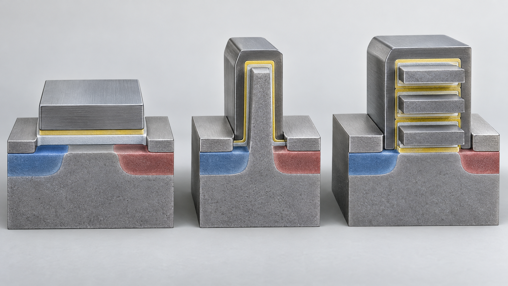
Shapes, colors and dimensions are illustrative. Consult the original schematic below for exact values and label correspondence.
View the original SVG schematic and exact annotations
Reading guide and original schematic labels: Surrounding the channel with more gate faces (conceptual diagram) / Cross-sections across the current. Blue = channel, orange = gate (with dielectric), grey = substrate or wall. / Planar / Gate on the / top face only / FinFET / Gate wraps / 3 faces (2012-) / Nanosheet / Gate wraps / all around (GAA) / Forksheet / Wall between n and / p (a proposal) / CFET / n / p / n and p stacked / (research) / The structures follow imec [Refs. 7-9] and IRDS 2023 [Ref. 10]. Dimensions and sheet counts are simplified. / The arrangement is this article's own and does not show any real product cross-section.
imec's 2022 technical article gives the reasons for moving from FinFET to nanosheet Sourced. To shrink standard-cell height, the number of fins per cell is reduced from three to two and then to one, and with fewer fins drive current falls and variability rises; making fins taller and thinner has its limits. Stacking nanosheets vertically gives a larger effective channel width in the footprint of a single fin. And because the nanosheet has the gate surrounding the whole channel (GAA), gate control is better at short gate lengths.
An example of how effective channel width (Weff) changes with structure Our calculation.
- FinFET (one fin): assume fin height 50 nm and fin width 6 nm. Weff = 2 × height + width = 2 × 50 + 6 = 106 nm
- Nanosheet (three sheets): assume each sheet 25 nm wide and 5 nm thick. Weff = 3 × (2 × width + 2 × thickness) = 3 × (50 + 10) = 180 nm
Assumptions and limits: all dimensions are assumptions of this article and not values for any real product. Sheet spacing, occupied area, corner effects and differences in how far the gate wraps are not considered. The calculation only shows the idea of gaining effective width by stacking more sheets in the same footprint.
imec lists four points where the nanosheet process differs from the FinFET Sourced: (1) the channel is made from an epitaxially grown multilayer of Si and SiGe (SiGe is a sacrificial layer removed later); (2) an inner spacer, a dielectric that isolates gate from source/drain, is made by laterally etching the SiGe (the article calls this the most complex module); (3) the sheets are released by selectively etching the SiGe, which requires control of stiction, where sheets stick together; (4) a replacement metal gate step puts work-function metal around and between the sheets.
3. Where things stand, as far as official sources show: started versus planned
| Company or body | What was published | Label |
|---|---|---|
| TSMC | 2 nm (N2) started volume production in 4Q 2025 (the company's page), with first-generation nanosheet transistors. N2P volume production is scheduled for 2H 2026. 3 nm (N3) FinFET went into volume production in 2022; N7 (2018) and N5 (2020) are FinFET | N2: Sourced (company announcement) / N2P: Not yet confirmed |
| TSMC (later generations) | A16: nanosheet transistors combined with a backside power rail; versus N2P, 8 to 10% higher speed at the same voltage, 15 to 20% lower power at the same speed, up to 1.10x chip density (company claims). Production-ready in 2H 2026. A14: versus N2, 10 to 15% higher speed at the same power or 25 to 30% lower power at the same speed, and more than 20% higher logic density (company claims). Scheduled for volume production in 2028. A13 is scheduled for 2029 | Not yet confirmed (performance figures are also company claims) |
| Samsung | Announced on 30 June 2022 that it had started initial production of 3 nm with GAA architecture. Its GAA is the MBCFET (Multi-Bridge-Channel FET), using nanosheets. Versus 5 nm, the first-generation 3 nm cuts power by up to 45%, raises performance 23% and cuts area 16%; the second generation is to cut power by up to 50%, raise performance 30% and cut area 35% (company claims and plans; the basis of comparison could not be confirmed in the release) | Initial production: Sourced (company announcement) / second generation: Not yet confirmed |
| Intel | The company's 18A page describes RibbonFET (GAA) and PowerVia (backside power) and states “In high-volume production in the United States”. Versus Intel 3.1, up to 18% higher performance at the same power, 38% lower power at the same performance, and 30% higher chip density (company claims) | Sourced (company statement; performance figures are company claims) |
| imec | Beyond nanosheets, it proposes and studies the forksheet (a dielectric wall between n and p) and the CFET (n and p stacked vertically), and examines two ways of making CFETs, monolithic and sequential. IRDS 2023 expects p and n devices to be integrated on top of each other beyond 2031 | Research and projection: Not yet confirmed |
TSMC's A14 comparison is against “N2” and A16's against “N2P”, so the bases differ and the numbers cannot be ranked against each other. Samsung's and Intel's baselines (5 nm, Intel 3.1) also differ. We found no company announcing volume production of a CFET in the official material checked. We did not confirm the current volume status of Samsung's GAA generations.
Samsung's 2018 conference paper (Bae et al.) says the MBCFET is made using 90% or more of the FinFET processes with only a few revised masks, and reports a subthreshold swing of 65 mV/dec at short gate length Sourced [Reference 13]. imec likewise says the nanosheet is a natural evolution of the FinFET, and that reuse of many process modules helped industry adoption Sourced. From the materials side, what is new is epitaxial growth of the Si/SiGe multilayer, selective removal of SiGe, and the gate materials that go between the sheets, and that is where the materials issues concentrate (our commentary).
4. Our calculation: if node names were dimensions, what would area do?
IRDS 2023 names gate pitch, metal pitch, fin pitch, gate length and 3D stacking capability as the key parameters for logic scaling, and says there is not yet a consensus on node naming across foundries and integrated device manufacturers Sourced. In 2020 imec stated that, in 7 nm chips, the contact pitch is as small as 57 nm and the tightest metal (M1 and M2) pitch is 40 nm Sourced (a general leading-edge example, not a particular company's value). So even a generation called “7 nm” has real pitches of tens of nanometers. IRDS projects that the physical gate length will saturate around 12 nm Not yet confirmed.
Suppose “3 nm” and “5 nm” were literally linear dimensions. What would area do? A simple calculation Our calculation.
- Area ratio: (3 / 5)² = 0.36, that is, a 64% reduction
- Samsung's announcement: versus 5 nm, the first-generation 3 nm has a 16% smaller area (0.84x) and the second generation a 35% smaller area (0.65x) Sourced (company claim and plan; the basis of comparison could not be confirmed in the release)
Assumptions and limits: real area reduction is decided by the combination of gate pitch, metal pitch and cell height (track count), not by the square of the name. This calculation only shows by orders of magnitude that the name is not a dimension; it does not judge whether Samsung's claim is right. Which area (standard cell, SRAM, whole chip) is meant could not be confirmed in the release either.
Intel's Bohr and Young discuss how to judge generations in their 2017 paper “CMOS Scaling Trends and Beyond” [Reference 21; only title and bibliographic details checked]. Because the meaning of a node name differs by company, comparisons should look not at names but at gate pitch, metal pitch, cell height and transistor density, together with how they were measured (our commentary).
5. Short-channel effects: a thin channel supports the power to stop current
As the gate shortens, the potential between source and drain is influenced strongly by the drain as well as the gate. The result is that current does not fully stop even when the gate voltage is lowered (the threshold falls and the subthreshold swing worsens): this is the short-channel effect (our commentary). Yan et al., “Scaling the Si MOSFET: from bulk to SOI to bulk” (IEEE TED, 1992) [Reference 17], and Colinge's review “Multiple-gate SOI MOSFETs” (2004) [Reference 18] deal with suppressing short-channel effects with a thin body (channel) and several gates (only titles and bibliographic details checked).
As a rough guide we calculate the natural length λ of a double-gate structure (a guide to the length at which short-channel effects begin) under conditions we set Our calculation.
- Equation: λ = √( (εSi / εox) × tSi × tox / 2 ) (tSi: channel thickness; tox: equivalent oxide thickness, EOT. A standard approximation; we did not check the equation in the papers)
- Assumptions: εSi = 11.7, εox = 3.9 (SiO2), EOT = 0.8 nm
- Channel thickness 5 nm: λ = √(3 × 5 × 0.8 / 2) = √6 = about 2.4 nm
- Channel thickness 7 nm: λ = √(3 × 7 × 0.8 / 2) = √8.4 = about 2.9 nm (about 1.18 times the 5 nm case)
- With EOT of 1.2 nm (channel 5 nm): λ = √(3 × 5 × 1.2 / 2) = √9 = 3.0 nm
Assumptions and limits: this is an idealised double-gate expression; it does not treat GAA (all-around gates) or the permittivities of real materials. All values are our assumptions. The point is that λ scales with the square root of channel thickness and EOT, so a thin channel and a thin gate dielectric support a short gate length.
6. A materials engineer's view (1): what to fit into the 10 nm gap between nanosheets
In a nanosheet device, the gate dielectric and work-function metal must go in between the stacked sheets as well. imec says it developed processes that reduce the vertical spacing between nanosheets to below 10 nm, to cut parasitic capacitance between gate and source/drain Sourced. In 2018 it also showed the importance of a scalable work-function metal, and that reducing the spacing between two neighboring sheets from 13 nm to 7 nm improved AC performance by 10% Sourced. IRDS says that, when devices are stacked, the spacing must be kept small while leaving enough space to deposit the gate dielectric and the Vt-tuning work-function metals Sourced.
With the sheet spacing at 10 nm, what goes into the gap? An estimate with thicknesses we assume Our calculation.
- Assumptions: sheet spacing 10 nm (an example at the level of imec's “below 10 nm”); gate dielectric (interfacial layer plus high-k) 2.5 nm thick (our assumption)
- Dielectric on both sides of the gap: 2.5 nm × 2 = 5 nm
- Space left for work-function metal and the like: 10 − 5 = 5 nm
- If different metals are used for n and p: metals with different thresholds have to be made separately within the same 5 nm
Assumptions and limits: the dielectric thickness is our assumption and not a real product's value. Considering the case where imec reduced the spacing to 7 nm, 10 − 5 = 5 nm becomes 7 − 5 = 2 nm, so with this assumed dielectric thickness almost no room is left for metal. In practice other designs, such as thinner dielectrics, would be needed (our commentary).
imec's article points to places in the nanosheet process where materials are especially hard Sourced.
- Inner spacer: filling the small cavities made by laterally etching SiGe with a dielectric needs high etch selectivity and precise lateral control. The article calls it the most complex module of the nanosheet flow
- Channel release: selectively removing SiGe to separate the sheets, with few Ge residues and low Si roughness, while avoiding stiction between sheets
- Replacement metal gate: making different work-function metals for n and p around and between the sheets. The article says this becomes more complicated still for the CFET
These are questions of which material to deposit, how thin, and where to leave it: selectivity in deposition and etching (our commentary). Atomic layer deposition and etching are covered in the series explainers on atomic layer deposition and on etching.
7. The gate dielectric: high-k and equivalent oxide thickness
Thinning the gate dielectric improves gate control but increases tunneling current through the film. So high-k materials (HfO2-based) with a higher permittivity than SiO2 are used: they can be physically thicker while giving the same capacitance electrically as a thin SiO2 (our commentary). Samsung presents itself as a pioneer of HKMG (high-k metal gate), FinFET, EUV and GAA Sourced. IRDS also lists the high-k metal gate among the means of boosting performance, and EOT scaling and a lower interface-trap density (Dit) among the means of preserving electrostatics Sourced. A review of the materials properties of high-k gate dielectrics is Wilk et al., “High-κ gate dielectrics: Current status and materials properties considerations” (J. Appl. Phys., 2001) [Reference 19; only title and bibliographic details checked].
The idea of equivalent oxide thickness (EOT), with values we assume Our calculation.
- Relation: EOT = physical thickness × (3.9 / κ) (3.9 is the relative permittivity of SiO2)
- Assumption: relative permittivity of the HfO2-based film κ = 20 (our assumption; it varies with crystal state and composition)
- HfO2-based thickness to get an EOT of 0.8 nm: 0.8 × 20 / 3.9 = about 4.1 nm (0.8 nm for SiO2)
- With κ = 25: 0.8 × 25 / 3.9 = about 5.1 nm
Assumptions and limits: a real gate dielectric has a thin SiO2-type interfacial layer against the Si, which adds to the EOT. κ is our assumption, not a real product's value. A film about 4 nm thick physically shows how much room the dielectric takes up in the “10 nm gap” of the previous section.
Lowering EOT (raising gate control) means thinning the physical dielectric in proportion. Yet, as the previous section showed, nanosheet spacing is being reduced, so the demand for a thinner dielectric and the demand for room for work-function metal arise in the same 10 nm gap (our commentary). imec reports, for the sequential CFET route, introducing an interface dipole between the HfO2 gate dielectric and the Si channel to shift the energy of HfO2 defect states Sourced. The reading is that the design of the interface between the film and Si, not only the high-k film itself, affects reliability (BTI and so on) (our commentary).
8. Doping: in a nanoscale channel, the number of dopant atoms is the issue
Sources and drains are doped heavily to lower resistance. imec says that as scaling shrank contact areas, source/drain contact resistance became a major issue, and it has responded by raising the doping level on the semiconductor side, optimizing the interface with the metal (a transition-metal silicide), and using wrap-around contacts made by ALD to enlarge the contact area Sourced. On the channel side, IRDS says that a dopant-free channel and low-variability work-function metals would reduce threshold-voltage variation Sourced. The paper by Asenov et al., “Simulation of intrinsic parameter fluctuations in decananometer and nanometer-scale MOSFETs” (IEEE TED, 2003), treats the discreteness of dopant atoms as a source of variability [Reference 20; only title and bibliographic details checked].
If dopants were put uniformly in the channel, how many atoms would be in it? Our calculation
- Channel volume: length 12 nm (the saturation level IRDS projects for physical gate length) × width 20 nm × thickness 5 nm (width and thickness are our assumptions) = 1,200 nm³
- At 1×1018 cm−3: 1×1018 × 1,200 × 10−21 = about 1.2 atoms
- At 1×1017 cm−3: about 0.12 atoms
- At 1×1019 cm−3: about 12 atoms
- Count fluctuation (Poisson rule of thumb): relative fluctuation about 1/√N: about 29% for N = 12 and about 91% for N = 1.2
Assumptions and limits: the concentrations are illustrative orders of magnitude, not a particular product's values, and the width and thickness are assumptions. The point is that when the channel volume falls to around a thousand cubic nanometers, dopants become a matter of chance: zero, one or two atoms rather than an average count, and device characteristics stop matching one another. This reads as one reason undoped channels are emphasised in FinFETs and nanosheets (our commentary).
9. Channel materials: Si, SiGe and two-dimensional semiconductors
IRDS 2023 expects the channel material to move from Si to SiGe, Ge and two-dimensional (2D) materials Not yet confirmed. imec likewise says that the sequential route to the CFET can use different channel materials by type: Si for n-type, SiGe or Ge for p-type, and even 2D materials such as WS2 Sourced.
Candidate 2D materials include transition-metal dichalcogenides (TMDs) such as MoS2. Radisavljevic et al. reported a single-layer MoS2 transistor in 2011 [Reference 24; only title and bibliographic details checked], and Liu et al. reviewed the promises and prospects of 2D transistors in Nature in 2021 [Reference 23; only title and bibliographic details checked]. A more recent example is Chung et al. at IEDM 2022, who reported a FET using a monolayer MoS2 nanosheet integrated in a GAA configuration Sourced.
| Item | Reported value | Conditions and level |
|---|---|---|
| Channel | Monolayer MoS2, thickness about 0.7 nm | Nanosheet FET in a GAA configuration. A single laboratory device |
| Gate length | 40 nm | Longer than the saturation level of physical gate length projected by the roadmap (about 12 nm, IRDS) |
| On-current | About 410 µA/µm | VDS = 1 V, per unit channel width. With a monolayer channel |
| On/off ratio | > 1×10⁸ | Same |
| Threshold voltage | About +1.4 V | DIBL reported as nearly zero |
| Other | Proposes that stacking several channel layers can give higher drive current. Examines the feasibility of modules needed for integration (stack and channel preparation, fin patterning, inner spacer, channel release, contact) | |
All Sourced (the abstract of Chung et al., IEDM 2022 [Reference 22]; a laboratory demonstration). This is neither a production specification nor a fair comparison with devices of other materials.
10. A materials engineer's view (2): laboratory best values are not production specifications
- A single-device demonstration is not uniformity across billions: Chung et al.'s values are characteristics of the reported device. Volume production needs billions of transistors to work together, so device-to-device variation and yield are what count. The official material used here gave no figures for the uniformity of 2D-channel devices in a production process
- The gate length is 40 nm: far longer than the saturation level projected by IRDS (about 12 nm), so performance at short gate length cannot be told from that paper
- The threshold voltage is about +1.4 V: the VDS in the measurement was 1 V. For logic use, the threshold may need tuning. This is an inference; it cannot be judged from the paper's abstract
- Difficulties as materials: growing large-area monolayers, transfer to or direct growth on the substrate, the interface with the gate dielectric and contact resistance to metal are generally discussed as challenges (our commentary). The official material used here gave no specific numbers for them
- CFET demonstrations should be read the same way: Liao et al. built a nanosheet-based monolithic CFET at a 48 nm gate pitch and reported a survival rate above 90% and an on/off ratio of six orders of magnitude for the stacked n-on-p devices (IEDM 2023). In 2024 they reported a working CFET inverter at the same 48 nm gate pitch Sourced. Both are research-stage demonstrations and do not mean volume production has started
When reading a company or institution announcement, first check at what scale (single device, test chip or volume production), and under what conditions, a value was obtained (our commentary).
11. What is still hard, and what could not be confirmed
(1) Volume-production timing and plans
TSMC has announced that N2 volume production has started, but N2P, A16, A14 and A13 are plans Not yet confirmed. We found no company announcing volume production of a CFET in the official material checked. IRDS 2023 expects stacking beyond 2031, but that is a projection.
(2) Disclosure of real dimensions
The official pages of TSMC, Samsung and Intel give no gate length, gate pitch or fin and sheet dimensions. The correspondence between node name and real dimensions could not be confirmed from official material. The dimensional figures in this article come from IRDS (projections), imec (general industry examples) and our own assumptions.
(3) Performance figures with unpublished bases of comparison
The “performance up x%”, “power down x%” and “area down x%” figures differ in their baseline (generation), and the details of the conditions are unpublished. They cannot be ranked across companies or generations.
(4) Industrialising 2D semiconductors
For 2D-channel devices, large-area uniformity, contact resistance, the interface with the gate dielectric and compatibility with volume processes could not be given specific numbers from the official material used here.
(5) Thermal budget and reliability
imec says that in the sequential route to the CFET, the top-tier processing temperature must be held to about 500°C or below, whereas gate-stack reliability and dopant activation usually need thermal steps of about 900°C Sourced. Reconciling the two is a challenge.
- Structure has moved toward surrounding the channel with more gate faces: FinFET (three faces; first commercial in 2012), nanosheet / GAA (all around), CFET (stacked) Sourced
- Volume production: TSMC announced the start of N2 (nanosheet), Samsung announced initial GAA production in 2022, and Intel's 18A page states high-volume production Sourced. TSMC's A14 (2028) and others are plans Not yet confirmed
- Node names are not dimensions: read as linear dimensions they would mean a 64% cut in area, whereas Samsung announced 16% for its first generation Our calculation
- A thinner channel holds a shorter gate: natural length scales with the square root of thickness and EOT (about 2.4 nm in our estimate) Our calculation
- Fitting dielectric and metal into the 10 nm gap between nanosheets is the materials crux. With our assumptions, a 7 nm gap leaves 2 nm for metal Our calculation
- Dopants become a matter of count: about 1.2 atoms in a 1,200 nm³ channel at 1018 cm−3 Our calculation
- 2D semiconductors are at the laboratory demonstration stage: a monolayer MoS2 GAA FET was reported with a 40 nm gate length and about 410 µA/µm (a single device) Sourced
12. Glossary
- Node name (process node)
- A generation label such as “3 nm” or “2 nm”. It does not correspond to real dimensions, and there is no consensus between companies.
- FinFET
- A structure with a fin-shaped channel that the gate wraps on three faces.
- GAA (gate-all-around)
- A structure in which the gate surrounds the whole channel. Nanosheet and nanowire types exist.
- Nanosheet
- A GAA structure with stacked thin plate-like channels. Samsung calls it MBCFET and Intel RibbonFET.
- Forksheet
- A nanosheet variant (from imec) with a dielectric wall between n and p so they can be placed closer.
- CFET
- Complementary FET: n-type and p-type transistors stacked vertically.
- Short-channel effect
- As the gate shortens, the drain's influence grows and current becomes harder to stop.
- Natural length λ
- A length, set by structure and dielectric, that guides at what gate length short-channel effects start.
- High-k / HKMG
- A gate dielectric of higher permittivity than SiO2 (HfO2-based) combined with a metal gate.
- EOT (equivalent oxide thickness)
- A gate dielectric's thickness expressed as the SiO2 thickness with the same capacitance.
- Work-function metal
- The gate metal that sets the threshold; made differently for n and p.
- Inner spacer
- The dielectric that isolates gate from source/drain in a nanosheet.
- Two-dimensional (2D) semiconductor
- A layered semiconductor such as MoS2, one to a few atomic layers thick.
- DIBL
- Drain-induced barrier lowering: the threshold falls as drain voltage rises. A measure of short-channel effects.
- IRDS
- The International Roadmap for Devices and Systems, led by the IEEE.
13. References (primary sources)
- TSMC, "2nm Technology" (start of N2 volume production in 4Q 2025; N2P plan; checked 9 October 2026) — tsmc.com
- TSMC, "A14 Technology" (A14 scheduled for 2028, A13 for 2029; checked 9 October 2026) — tsmc.com
- TSMC, "A16 Technology" (production-ready in 2H 2026; checked 9 October 2026) — tsmc.com
- Samsung Electronics, "Samsung Begins Chip Production Using 3nm Process Technology With GAA Architecture", 30 June 2022 — news.samsung.com
- Samsung Semiconductor, "Process Technology" (introduction of HKMG, FinFET, EUV and GAA; checked 9 October 2026) — semiconductor.samsung.com
- Intel, "Intel 18A" (RibbonFET, PowerVia and the volume-production statement; checked 9 October 2026) — intel.com
- imec, "Imec puts complementary FET (CFET) on the logic technology roadmap", 16 June 2022 — imec-int.com
- imec, "A view on the logic technology roadmap", 22 September 2020 — imec-int.com
- imec, "Entering the nanosheet transistor era", 11 February 2022 — imec-int.com
- IEEE IRDS, "International Roadmap for Devices and Systems 2023: More Moore" (PDF) — irds.ieee.org
- Hisamoto et al., "FinFET-a self-aligned double-gate MOSFET scalable to 20 nm", IEEE Trans. Electron Devices 47, 2320 (2000) (only title and bibliographic details checked) — doi.org
- Loubet et al., "Stacked nanosheet gate-all-around transistor to enable scaling beyond FinFET", Symp. VLSI Technology 2017 (only title and bibliographic details checked) — doi.org
- Bae et al., "3nm GAA Technology featuring Multi-Bridge-Channel FET for Low Power and High Performance Applications", IEEE IEDM 2018 — doi.org
- Liao et al., "Complementary Field-Effect Transistor (CFET) Demonstration at 48nm Gate Pitch for Future Logic Technology Scaling", IEEE IEDM 2023 — doi.org
- Liao et al., "First Demonstration of Monolithic CFET Inverter at 48nm Gate Pitch Toward Future Logic Technology Scaling", IEEE IEDM 2024 — doi.org
- Ritzenthaler et al., "Comparison of Electrical Performance of Co-Integrated Forksheets and Nanosheets Transistors for the 2nm Technological Node and Beyond", IEEE IEDM 2021 (only title and bibliographic details checked; imec's article reports its results) — doi.org
- Yan et al., "Scaling the Si MOSFET: from bulk to SOI to bulk", IEEE Trans. Electron Devices 39, 1704 (1992) (only title and bibliographic details checked) — doi.org
- Colinge, "Multiple-gate SOI MOSFETs", Solid-State Electron. 48, 897 (2004) (a review; only title and bibliographic details checked) — doi.org
- Wilk et al., "High-κ gate dielectrics: Current status and materials properties considerations", J. Appl. Phys. 89, 5243 (2001) (a review; only title and bibliographic details checked) — doi.org
- Asenov et al., "Simulation of intrinsic parameter fluctuations in decananometer and nanometer-scale MOSFETs", IEEE Trans. Electron Devices 50, 1837 (2003) (only title and bibliographic details checked) — doi.org
- Bohr and Young, "CMOS Scaling Trends and Beyond", IEEE Micro 37(6) (2017) (only title and bibliographic details checked) — doi.org
- Chung et al., "First Demonstration of GAA Monolayer-MoS2 Nanosheet nFET with 410µA/µm ID at 1V VD at 40nm gate length", IEEE IEDM 2022 — doi.org
- Liu et al., "Promises and prospects of two-dimensional transistors", Nature 591, 43 (2021) (a review; only title and bibliographic details checked) — doi.org
- Radisavljevic et al., "Single-layer MoS2 transistors", Nature Nanotechnol. 6, 147 (2011) (only title and bibliographic details checked) — doi.org
14. Claim-to-source audit
| Claim in the text | Basis | Label |
|---|---|---|
| TSMC: N2 began volume production in 4Q 2025 with first-generation nanosheet transistors; N2P scheduled for volume production in 2H 2026; N3 FinFET in 2022, N5 (2020) and N7 (2018); 16nm FinFET risk production in 2013 | Reference 1 https://www.tsmc.com/english/dedicatedFoundry/technology/logic/l_2nm | Sourced |
| TSMC A16: nanosheet plus backside power rail, versus N2P 8 to 10% higher speed at the same voltage, 15 to 20% lower power at the same speed, up to 1.10x density, production-ready in 2H 2026. A14: versus N2 10 to 15% higher speed or 25 to 30% lower power, more than 20% higher logic density, volume production scheduled for 2028; A13 for 2029 (performance figures are company claims) | Reference 2 https://www.tsmc.com/english/dedicatedFoundry/technology/logic/l_A14 Reference 3 https://www.tsmc.com/english/dedicatedFoundry/technology/logic/l_A16 | Not yet confirmed |
| Samsung (30 June 2022): initial production of 3nm with GAA, the MBCFET (nanosheet); versus 5nm the first generation cuts power by up to 45%, raises performance 23% and cuts area 16%, the second generation 50%, 30% and 35%. The company introduced as a pioneer of HKMG, FinFET, EUV and GAA | Reference 4 https://news.samsung.com/global/samsung-begins-chip-production-using-3nm-process-technology-with-gaa-architecture Reference 5 https://semiconductor.samsung.com/foundry/process-technology/ | Sourced |
| Intel 18A page: RibbonFET (GAA) and PowerVia, a statement of high-volume production in the United States, and versus Intel 3.1 up to 18% higher performance, 38% lower power and 30% higher density (company claims) | Reference 6 https://www.intel.com/content/www/us/en/foundry/process/18a.html | Sourced |
| imec: first commercial FinFET (22 nm) in 2012; the FinFET wraps three faces; beyond 5nm the FinFET gives insufficient control; nanosheets as a natural evolution of the FinFET; the problems of drive current and variability as fins are reduced; the four nanosheet process points (Si/SiGe multilayer epitaxy, inner spacer, channel release, replacement metal gate); spacing reduced to below 10 nm; AC performance 10% better from 13 nm to 7 nm; forksheet with 17 nm n-p space and subthreshold swing of 66 to 68 mV; the monolithic and sequential CFET routes; the sequential thermal budget (about 500 C versus 900 C); the interface dipole between HfO2 and Si | Reference 7 https://www.imec-int.com/en/articles/imec-puts-complementary-fet-cfet-logic-technology-roadmap Reference 8 https://www.imec-int.com/en/articles/view-logic-technology-roadmap Reference 9 https://www.imec-int.com/en/articles/entering-nanosheet-transistor-era-0 | Sourced |
| imec: in 7 nm chips the contact pitch is 57 nm and the M1/M2 metal pitch 40 nm. Measures against source/drain contact resistance (doping level, interface, wrap-around contacts) | Reference 8 https://www.imec-int.com/en/articles/view-logic-technology-roadmap | Sourced |
| IRDS 2023: no consensus on node naming; key parameters (gate pitch, metal pitch, fin pitch, gate length); physical gate length projected to saturate near 12 nm; p and n integrated on top of each other beyond 2031; FinFET until 2025 and the transition to GAA starting in 2022; channel material moving from Si to SiGe, Ge and 2D; high-k metal gate; EOT scaling and lower Dit; dopant-free channel; the sheet spacing and the room for dielectric and work-function metals | Reference 10 https://irds.ieee.org/images/files/pdf/2023/2023IRDS_MM.pdf | Sourced |
| Bae et al. (Samsung, IEDM 2018): the MBCFET is made with 90% or more of the FinFET processes and a few revised masks; subthreshold swing of 65 mV/dec at short gate length | Reference 13 https://doi.org/10.1109/IEDM.2018.8614629 | Sourced |
| Liao et al. (IEDM 2023 and 2024): nanosheet-based monolithic CFET at 48 nm gate pitch, survival rate above 90% and six orders of magnitude of on/off ratio for stacked n-on-p devices; in 2024 a working CFET inverter | Reference 14 https://doi.org/10.1109/IEDM45741.2023.10413672 Reference 15 https://doi.org/10.1109/IEDM50854.2024.10873334 | Sourced |
| Chung et al. (IEDM 2022): a GAA nanosheet FET with monolayer MoS2 (about 0.7 nm), 40 nm gate length, on-current about 410 uA/um (VDS = 1 V), on/off ratio above 1e8, threshold about +1.4 V, nearly zero DIBL, higher drive current proposed by stacking, and the feasibility of integration modules examined | Reference 22 https://doi.org/10.1109/IEDM45625.2022.10019563 | Sourced |
| FinFET (Hisamoto et al. 2000), stacked nanosheets (Loubet et al. 2017), the multi-gate idea (Yan et al. 1992, Colinge 2004), the review of high-k (Wilk et al. 2001), intrinsic variability (Asenov et al. 2003), comparison of nodes (Bohr and Young 2017), the outlook for 2D transistors (Liu et al. 2021), single-layer MoS2 transistors (Radisavljevic et al. 2011) and forksheet versus nanosheet (Ritzenthaler et al. 2021): only titles and bibliographic details checked | Reference 11 https://doi.org/10.1109/16.887014 Reference 12 https://doi.org/10.23919/VLSIT.2017.7998183 Reference 16 https://doi.org/10.1109/IEDM19574.2021.9720524 Reference 17 https://doi.org/10.1109/16.141237 Reference 18 https://doi.org/10.1016/j.sse.2003.12.020 Reference 19 https://doi.org/10.1063/1.1361065 Reference 20 https://doi.org/10.1109/TED.2003.815862 Reference 21 https://doi.org/10.1109/MM.2017.4241347 Reference 23 https://doi.org/10.1038/s41586-021-03339-z Reference 24 https://doi.org/10.1038/nnano.2010.279 | Sourced |
| The effective channel widths (FinFET 106 nm, three nanosheets 180 nm); (3/5)^2 = 0.36 (a 64% cut); natural length lambda (about 2.4, 2.9 and 3.0 nm); the 10 nm sheet gap budget (5 nm dielectric, 5 nm for metal and the like, 2 nm at 7 nm); the HfO2-based thickness for an EOT of 0.8 nm (about 4.1 nm at kappa 20, about 5.1 nm at 25); the dopants in a 1,200 nm^3 channel (about 1.2 at 1e18 cm^-3, about 12 at 1e19, about 0.12 at 1e17) and the fluctuations (about 91%, about 29%) | Our calculation. Dimensions, kappa, concentrations and dielectric thicknesses are assumptions of this article, not real product values. The natural-length expression is a standard approximation that we did not check in the papers | Our calculation |
| The volume production of TSMC's N2P, A16, A14 and A13, Samsung's second-generation 3nm, the timing of CFET introduction in IRDS (beyond 2031) and the saturation of physical gate length (about 12 nm) | Company plans and institutional projections, not results (an outlook) | Not yet confirmed |
| The reading that GAA has been introduced as an extension of the FinFET; the arrangement that comparison of nodes should look at pitches, cell height and density rather than names; the arrangement that materials difficulty concentrates in deposition and etch selectivity; the arrangement that EOT scaling and the gap problem are solved together; the reading that dopants become a matter of count; the way to read the numbers for 2D semiconductors | Our commentary built on the published material. It is not a view stated by any company or institution | Commentary |
| The idea that a threshold of about +1.4 V may need tuning before logic use | A weakly supported idea, marked Inference. The paper's abstract does not settle it | Commentary |
| The real gate length, gate pitch and sheet dimensions of TSMC, Samsung and Intel; a company announcing CFET volume production; Samsung's current GAA generation status; uniformity of 2D-channel devices in volume production; the bases of comparison for companies' performance figures | These could not be confirmed in official sources within the scope of this article, so none is stated | Commentary |
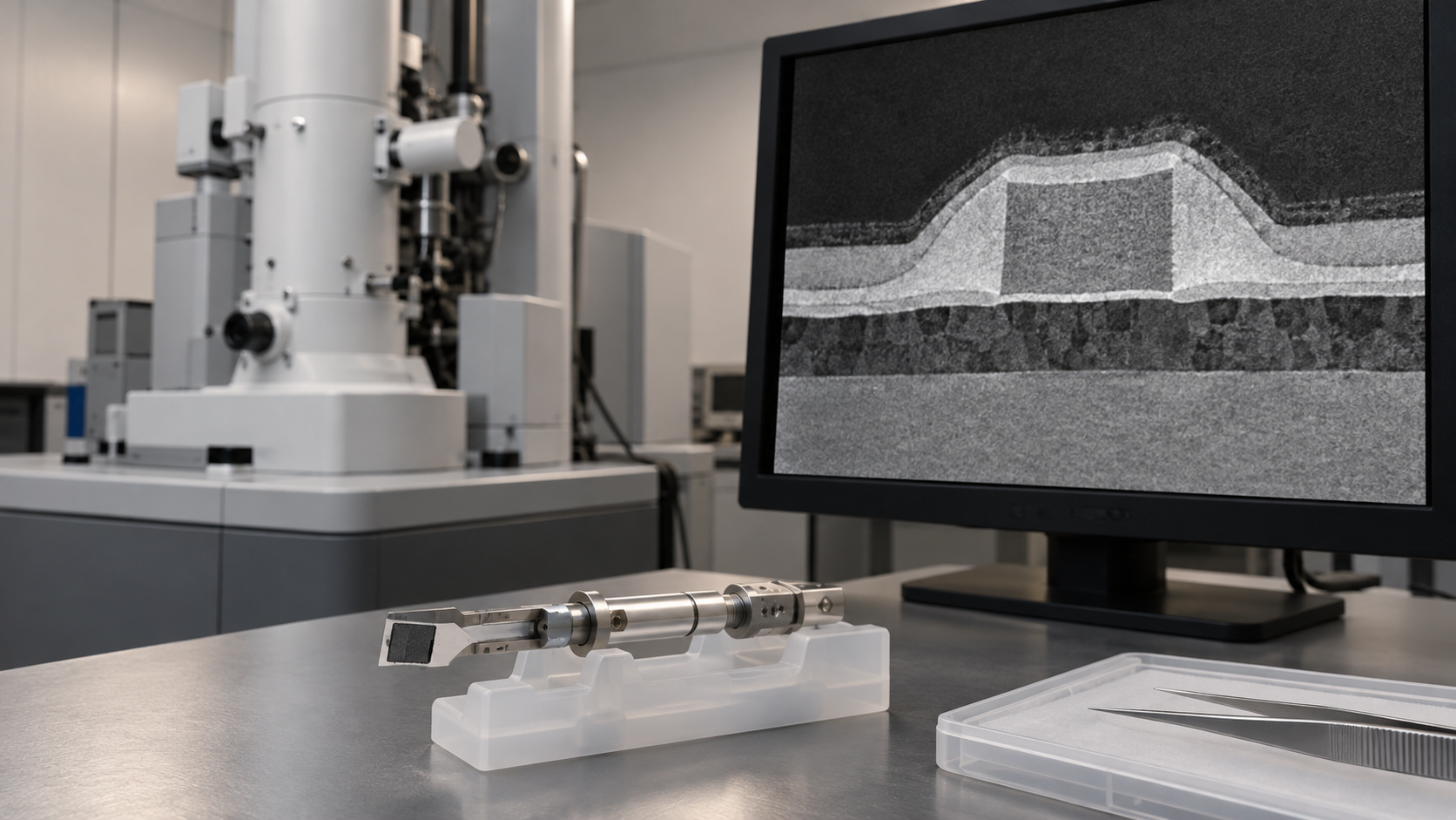
| That Figs. 1, 2, 5 and 8 are conceptual drawings, that Figs. 3, 4, 5 and 7 are drawings that include our calculation, and that the hero image and Fig. 6 are AI-generated images | Our note | Commentary |
Last updated 9 October 2026 (company announcements checked the same day). Sources are limited to primary material (the official pages of TSMC, Samsung, Intel and imec, the IRDS 2023 roadmap, and conference and peer-reviewed papers). Because the article includes structural readings and materials-design interpretations, those are marked as Commentary and kept separate from sourced fact. The real gate length, pitches and sheet dimensions of each company, the start of CFET volume production, Samsung's current generation status, the uniformity of 2D-channel devices in volume production and the bases of comparison for performance figures are not stated here because no published primary source could be confirmed. Performance figures and plans are each company's own statements, and a single-device laboratory value is not presented as the performance of a production part. All figures are explanatory concept graphics. Figs. 1, 2, 5 and 8 are vector drawings, Figs. 3, 4, 5 and 7 are vector drawings that include our calculations, and the hero image and Fig. 6 are AI-generated images, and none of them shows a real cross-section, micrograph or physical product.