TECHNOLOGY EXPLAINER
Plasmonics and Nanophotonics
— bending, concentrating and sensing light with structures smaller than its wavelength
Gold and silver nanoparticles look red or purple because the free electrons in the metal oscillate collectively with the light (plasmon resonance). This resonance can gather light into regions far smaller than its wavelength, and is used in sensors, optical elements, and to raise the efficiency of light emission and solar cells. Seen from the materials side, what sets how sharp and strong the resonance is, is the “quality” of the metal (surface smoothness, crystallinity, adhesion layer) and control of shape, size and gap dimensions; and, as a second stream that avoids metal loss, metasurfaces made of high-index transparent materials such as TiO2 are approaching practical use. This article covers localised surface plasmon resonance, gold, silver and alternative materials, nanoantennas, metasurfaces and uses. Where it overlaps with the photodetector explainer in the optical communications series and the surface plasmon resonance and Raman/SERS explainers in the biosensor series, it refers to them in the text.

- What plasmonics and nanophotonics are, in three points
- Localised surface plasmon resonance: the “colour” of metal nanoparticles
- Our calculation: where the resonance sits, and how “dull” it is
- Materials: gold, silver and alternatives
- A materials engineer's view (1): the “quality” of the metal sets the resonance
- Nanoantennas: gathering light onto a molecule
- A materials engineer's view (2): distance is set by a nanometre-thick film
- Metasurfaces: making a lens from a flat plate
- A materials engineer's view (3): moving to low-loss transparent materials
- Uses: sensing, optical elements and light extraction
- What this article could not confirm, and a summary
- Glossary / References / Claim-to-source audit
Sourced = stated in a published document, paper or company announcement (link given)
Our calculation = a value this article derived from assumptions it states
Not yet confirmed = a plan, outlook or matter not yet settled
Structural readings and materials-design interpretations are marked separately as Commentary.
This article explains materials, principles and evaluation. It does not rank any product or company.
Performance values differ in method, sample and conditions from paper to paper, so please do not set them side by side to rank them. Laboratory values are not the performance of production items. Company announcements are marked as company statements.
Sensing with surface plasmon resonance on thin films is covered in our explainer on surface plasmon resonance, enhancement of Raman scattering in our explainer on Raman spectroscopy and SERS, and light-receiving devices in our explainer on photodetectors.
1. What plasmonics and nanophotonics are, in three points
- What it does: Barnes, Dereux and Ebbesen published in 2003 a review titled “Surface plasmon subwavelength optics” (from the title). Plasmonics couples the oscillation of electrons at a metal surface to light so as to handle light in regions smaller than its wavelength Sourced. The broader field of confining and manipulating light in small regions is nanophotonics, which also includes dielectric structures with no metal
- What it is made of: The leading materials are gold and silver (Johnson and Christy's classic paper measured the optical constants n and k of copper, silver and gold over 0.5–6.5 eV). Because metal loss is large, alternative materials (alloys, heavily doped semiconductors and others) are also being examined Sourced
- What is hard: The resonance is dulled by loss (our calculation gives a sharpness index of about 9), the quality of the metal film and the adhesion layer change performance greatly, and the distance to a molecule must be controlled to the nanometre Sourced (Chapters 3–7)
The strength of plasmonics is that light can be gathered into a tiny region; its weakness is that metal loss dulls the resonance; and both are set by the quality of the material. Even for the same gold, film roughness or an adhesion layer changes the resonance. That is why, as a way to avoid loss, metasurfaces made of transparent dielectrics with a high refractive index (TiO2 and the like) are approaching practical use (Commentary).
2. Localised surface plasmon resonance: the “colour” of metal nanoparticles
When light strikes a metal nanoparticle, the free electrons inside oscillate together with the light's electric field, and strong absorption and scattering occur at particular wavelengths. This is localised surface plasmon resonance (LSPR) (Commentary). The review by Kelly et al. describes how the optical properties of metal nanoparticles change with size, shape and dielectric environment; the features of the dipole and quadrupole plasmon resonances of spherical particles; analytical and numerical methods for calculating extinction and scattering cross-sections and local fields of non-spherical particles; and applications to triangular silver particles and related shapes Sourced.
- Size: Link and El-Sayed studied the plasmon absorption of gold nanoparticles 9, 15, 22, 48 and 99 nm in diameter in water and found that the bandwidth increases with decreasing size in the intrinsic size region (below 25 nm) and with increasing size in the extrinsic region (above 25 nm). They concluded from the homogeneous size distribution that the broadening is homogeneous, and calculated a dephasing time of the coherent plasmon oscillation of less than 5 fs Sourced.
- Shape: Nikoobakht and El-Sayed made gold nanorods with aspect ratios from 1.5 to 10 by a seed-mediated growth method, with surface plasmon absorption maxima between 600 and 1300 nm. They state that using a seed capped with CTAB (hexadecyltrimethylammonium bromide) reduced the formation of non-cylindrical rods and the fraction of spherical particles Sourced.
- Environment: The resonance position moves with the surrounding refractive index, which is the principle of LSPR sensors. This is covered in our explainer on surface plasmon resonance (the LSPR section), and enhancement in Raman spectroscopy in our explainer on Raman spectroscopy and SERS.
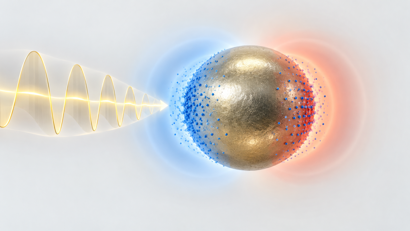
Shapes, colors and dimensions are illustrative. Consult the original schematic below for exact values and label correspondence.
View the original SVG schematic and exact annotations
Reading guide and original schematic labels: Localised surface plasmon resonance (LSPR): concept / The light's field makes the electron cloud slosh / metal particle / light field / The electron cloud shifts to one side / and oscillates under the restoring force / At the resonant / wavelength: / strong absorption, scattering / A strong local field forms around the particle (nanoantenna, Ch. 6) / Shape moves the resonance (schematic) / wavelength → / sphere / rod (long axis) / For rods, a higher aspect ratio shifts to longer wavelength / Note: conceptual; the shape, position and strength of spectra are not shown. / Based on Kelly et al., Link et al. and Nikoobakht et al. [Ref. 2-4]; not the spectrum of any real particle.
3. Our calculation: where the resonance sits, and how “dull” it is
Convert the plasmon absorption maxima reported by Nikoobakht and El-Sayed (600–1300 nm) to energy by E ≈ 1239.84 ÷ λ Our calculation.
- 600 nm: about 2.07 eV / 1300 nm: about 0.95 eV
- In other words, changing the aspect ratio from 1.5 to 10 moves the resonance energy by a factor of about 2.2 (from visible to near infrared)
From the report of Link and El-Sayed (dephasing time T2 below 5 fs), estimate the linewidth of the resonance. For a Lorentzian spectrum the homogeneous linewidth (full width at half maximum) is Γ = 2ℏ ÷ T2 (a relation we assume). Take ℏ ≈ 0.658 eV·fs Our calculation.
- Γ ≥ 2 × 0.658 ÷ 5 ≈ 0.26 eV (as T2 is below 5 fs, the linewidth is at least this)
- If the resonance centre is assumed to be 520 nm (about 2.38 eV, an assumption), the width in wavelength is Δλ ≈ 520² × 0.26 ÷ 1239.84 ≈ about 57 nm
- The index of resonance sharpness (Q factor) is 2.38 ÷ 0.26 ≈ about 9
Assumptions and limits: The centre of 520 nm is an assumption. Real resonances broaden further through size distribution and shape variation. Even so, a Q factor of about 10 shows that the plasmon resonance of a metal is a “dull” resonance, which is one reason dielectric nanostructures that can reduce loss (Chapter 9) attract attention (Commentary).
4. Materials: gold, silver and alternatives
The optical constants of metals are the starting point of plasmonic design. Johnson and Christy (1972) obtained the optical constants n and k of copper, silver and gold over the range 0.5–6.5 eV from reflection and transmission measurements on vacuum-evaporated thin films at room temperature. Of film thicknesses of 185–500 Å, results for 250–500 Å were independent of thickness and unchanged by vacuum annealing or aging in air; the estimated error in n and k was less than 0.02 over most of the spectral range Sourced.
The review by West et al. describes plasmonics as a field that merges optics and nanoelectronics by confining light of relatively large free-space wavelength to the nanometre scale, thereby enabling novel devices, while current plasmonic devices at telecommunication and optical frequencies face significant challenges owing to losses in the constituent materials. It compares metals, metal alloys and heavily doped semiconductors, evaluates each by quality factors defined for each class of device, and outlines an approach for realising optimal plasmonic material properties for specific frequencies and applications Sourced. Khurgin states that metal losses affect the performance of every plasmonic or metamaterial structure, and dealing with them will determine the degree to which these structures will find practical applications Sourced.
5. A materials engineer's view (1): the “quality” of the metal sets the resonance
- Deposition conditions: McPeak et al. point out that many plasmonics researchers deposit metals under the wrong conditions, severely limiting performance unnecessarily. They give simple rules and recipes, collected from the surface-science literature, for depositing high-quality plasmonic films of aluminium, copper, gold and silver with commonly available equipment (a thermal evaporator) Sourced.
- Surface smoothness: Nagpal et al. note that surface roughness and other inhomogeneities have limited surface-plasmon propagation in real plasmonic devices. They combined template stripping with patterned silicon substrates to obtain ultrasmooth pure metal films with grooves, bumps, pyramids, ridges and holes, and report that measured surface-plasmon propagation lengths approach the theoretical values for perfectly flat films Sourced.
- Adhesion layer: Habteyes et al. showed that an ultrathin (about 2 nm) titanium (Ti) adhesion layer shortens the plasmon dephasing time of gold nanorods significantly and cuts the plasmon scattering amplitude drastically (chemical interface damping), whereas molecular adhesion (a sulfur–gold bond through mercaptopropyl trimethoxysilane) showed no observable plasmon damping Sourced. This overlaps with the adhesion-layer discussion for gold films in our explainer on surface plasmon resonance.
- How to read it: Plasmonic performance can change greatly with the quality of the film (grain boundaries and roughness) and the interface (adhesion layer), more than with the kind of metal (Commentary).
6. Nanoantennas: gathering light onto a molecule
A nanoantenna is a structure that, like a radio antenna, receives light and creates a strong local electric field in a tiny region. Novotny and van Hulst published a review titled “Antennas for light” in 2011 (from the title), and Kinkhabwala et al. reported in 2009 large single-molecule fluorescence enhancements produced by a bowtie nanoantenna (from the title) Sourced.
In 2006 Anger, Bharadwaj and Novotny studied the fluorescence rate of a single molecule as a function of its distance to a laser-irradiated gold nanoparticle. The local-field enhancement increases the excitation rate, whereas nonradiative energy transfer to the particle lowers the quantum yield (quenching); because of these competing effects, previous experiments showed either enhancement or quenching alone. By varying the distance they gave the first experimental demonstration of the continuous transition from fluorescence enhancement to quenching, which they say cannot be explained by treating the particle as a polarizable sphere in the dipole approximation Sourced.
7. A materials engineer's view (2): distance is set by a nanometre-thick film
- Designing the thickness between molecule and antenna: The result of Anger et al. (a continuous transition from enhancement to quenching) shows that the distance between metal and fluorescent molecule is a design variable that decides the effect Sourced. The design therefore places on the metal a spacer layer whose thickness is controlled in units of nanometres (an oxide film, a polymer, a molecular film) (Commentary; this article has not confirmed a specific optimum distance).
- Controlling film thickness: Nanometre control of thickness belongs to our explainers on atomic layer deposition and on nano-coatings and thin films. What matters here is film uniformity: a pinhole becomes a place where metal and molecule touch directly and quench (Commentary).
- Hot spots are also sensitive to material defects: As in the gap of a bowtie, a strong field forms in a very small region of the gap. If the gap dimension is off by a few nanometres the enhancement can change by orders of magnitude, so lithographic precision and the metal's grain boundaries and roughness decide reproducibility (Commentary; this article has not confirmed concrete values).
- Heat: The loss of metal absorbing light becomes heat. For uses with intense light, deformation or alteration of the structure by heating is also a design item (Commentary; this article has not confirmed concrete values).
8. Metasurfaces: making a lens from a flat plate
In 2011 Yu et al. showed that abrupt phase changes over the scale of the wavelength give new degrees of freedom for shaping light beams. A two-dimensional array of optical resonators with spatially varying phase response and subwavelength separation imprints phase discontinuities on light crossing the interface between two media. In optically thin arrays of metallic antennas on silicon they observed anomalous reflection and refraction in excellent agreement with generalized laws derived from Fermat's principle Sourced. This is the starting point of metasurfaces. Arbabi et al. reported dielectric metasurfaces that control phase and polarisation completely with subwavelength spatial resolution and high transmission (from the title) Sourced.
The review by Kuznetsov et al. says that, apart from plasmonic metals, a new branch of nanophotonics has emerged that manipulates the strong electric and magnetic Mie resonances in dielectric nanoparticles of high refractive index, and that in the design of optical nanoantennas and metasurfaces dielectrics offer the opportunity of reducing dissipative losses and achieving large resonant enhancement of both electric and magnetic fields Sourced.
Apply the Abbe formula (a guide to the diffraction-limited spot size ≈ λ ÷ (2 × NA)) to the report of Khorasaninejad et al. (numerical aperture NA = 0.8; wavelengths 405, 532 and 660 nm) Our calculation.
- 405 nm: about 253 nm / 532 nm: about 333 nm / 660 nm: about 413 nm
Assumptions and limits: The Abbe formula is a guide; actual spot sizes differ with the beam shape and the definition used for evaluation. These are not the focal sizes reported by the paper.
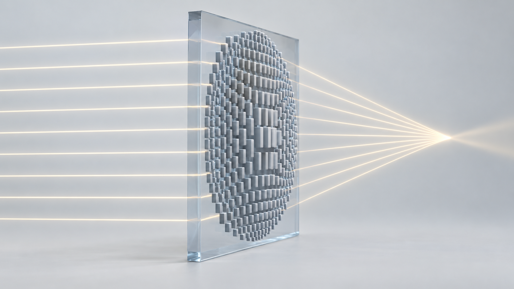
Shapes, colors and dimensions are illustrative. Consult the original schematic below for exact values and label correspondence.
View the original SVG schematic and exact annotations
Reading guide and original schematic labels: The idea of a metalens (concept) / glass substrate / flat wavefront / focus / Pillar width sets / the optical delay / A reported TiO₂ metalens / (Khorasaninejad et al. 2016) / NA = 0.8 / Diffraction-limited focusing / at 405, 532 and 660 nm / Efficiency 86, 73, 66% / Magnification up to 170x / Definition and conditions / of efficiency depend on the paper / Note: the left is conceptual and does not show the number, size or layout of pillars; / the right gives values reported by Khorasaninejad et al. [Ref. 15], a laboratory prototype.
In 2016 Khorasaninejad et al. showed that high-aspect-ratio titanium dioxide (TiO2) metasurfaces can be fabricated and designed as metalenses with NA = 0.8. They demonstrated diffraction-limited focusing at 405, 532 and 660 nm with efficiencies of 86, 73 and 66%, the ability to resolve nanoscale features separated by subwavelength distances, and magnification as high as 170×, with image quality comparable to a state-of-the-art commercial objective Sourced (a laboratory prototype; the definition and conditions of efficiency are those of the paper).
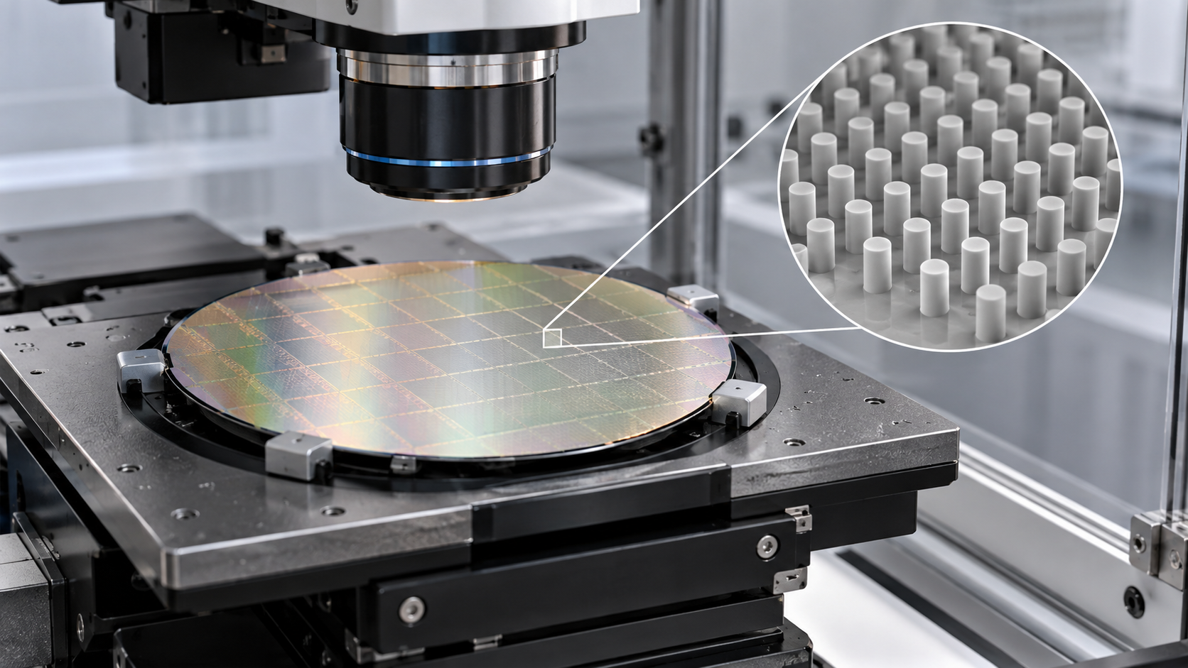
As an example of practical use, a joint announcement by the metalens company Metalenz and STMicroelectronics (9 June 2022) says that ST's VL53L8 direct time-of-flight (dToF) sensor is the market debut of meta-optics devices developed through their partnership, that this is the first time metasurface technology is commercially available and used in consumer devices, and that the planar metasurface optics are manufactured on silicon wafers alongside electronics in ST's front-end fabs (a company announcement) Sourced. An announcement of 10 July 2025 quotes ST as saying that since 2022 it has shipped well over 140 million metasurface optics and FlightSense modules using Metalenz IP, using a 300 mm semiconductor manufacturing process (a company statement, not an independent confirmation) Sourced. An announcement by Metalenz of 26 June 2023 says that UMC has released Metalenz's metasurface manufacturing process to production in its 12-inch wafer fab (a company announcement) Sourced.
9. A materials engineer's view (3): moving to low-loss transparent materials
- Avoiding loss: The plasmon of a metal is lossy (Chapter 3), and Kuznetsov et al. say that dielectrics can reduce dissipative losses Sourced. For uses such as metasurfaces, where light is transmitted, metal loss is a major disadvantage, hence the move to dielectrics (Commentary).
- Material requirements: What Khorasaninejad et al. used was TiO2, a material transparent in the visible, of high refractive index, and capable of forming high-aspect-ratio pillars. It is the same material as in our explainer on titanium dioxide and photocatalysis, and optical constants that change with crystal form and deposition method are also common to both (Commentary).
- Processing requirements: High-aspect-ratio fine pillars call for a combination of ALD (our explainer on atomic layer deposition) and fine patterning (explainers on lithography and EUV and on etching). The abstract of Khorasaninejad et al. says high-aspect-ratio TiO2 structures can be fabricated, but this article has not confirmed the fabrication details.
- Manufacturability: The company announcements say that metasurfaces are made in 300 mm and 12-inch wafer semiconductor processes (above). One can organise this as metasurfaces operating as “optical elements that a semiconductor line can make”, but yield, cost and environmental robustness could not be confirmed in published primary sources.
- Where metal remains necessary: Strong local fields and molecular sensing (LSPR, SERS) need the resonance of a metal's free electrons. Uses where loss is the problem move to dielectrics, and uses whose purpose is to concentrate the field stay with metal, a division of labour that is advancing (Commentary).
10. Uses: sensing, optical elements and light extraction
(1) Sensing
Haes and Van Duyne (2002) reported a nanoscale optical biosensor based on the localised surface plasmon resonance of triangular silver nanoparticles (from the title; details in our explainer on surface plasmon resonance) Sourced. Nagpal et al. show, with structures made by template stripping, Raman scattering enhancements above 107 Sourced (how to read enhancement factors is in our explainer on Raman spectroscopy and SERS).
(2) Optical elements
Besides metasurface optics (Chapter 8), Yu et al. demonstrated, with arrays of metallic antennas that change phase abruptly, among other things the generation of optical vortices Sourced.
(3) Light extraction and solar cells
Okamoto et al. reported in 2004 surface-plasmon-enhanced light emitters based on InGaN quantum wells (from the title), and Atwater and Polman reviewed plasmonics for improved photovoltaic devices in 2010 (from the title) Sourced. The idea is to raise light extraction or absorption with metal nanostructures, but it is traded off against the loss problem of Chapter 3, and the level of practical use and adoption in production items could not be confirmed in primary sources in this article. The materials of light-receiving devices (photodiodes and the like) are covered in our explainer on photodetectors.
11. What this article could not confirm, and a summary
- Specific resonance wavelengths, optimum distance and enhancement factors: Within the sources this article could confirm, no numbers are quoted for the resonance wavelength of gold and silver nanoparticles (for example gold nanospheres), the distance of maximum fluorescence enhancement or the enhancement of a bowtie (the 520 nm used in the calculation is an assumption).
- Papers confirmed by title only: The review of Barnes et al., the paper of Arbabi et al., the review of Novotny and van Hulst, the paper of Kinkhabwala et al., the paper of Okamoto et al. and the review of Atwater and Polman were checked by title only.
- Metasurface fabrication details, yield, cost and robustness: We did not confirm the fabrication details of Khorasaninejad et al., or the yield, cost and environmental robustness of company production items.
- Company shipment numbers: “well over 140 million” is ST's statement and not an independent confirmation.
- Adoption in light extraction and solar cells: The state of adoption in production items could not be confirmed in primary sources.
- Performance of alternative materials: The individual figure-of-merit values of the alternative materials compared by West et al. are not quoted.
- Degradation of silver: How fast silver nanostructures degrade by oxidation or sulfidation was not confirmed in this article.
- The “colour” of metal nanoparticles comes from the collective oscillation of free electrons (LSPR). Size, shape and surroundings move the resonance Sourced. Gold nanorods with aspect ratios of 1.5–10 have absorption maxima at 600–1300 nm Sourced
- The resonance is dulled by loss. From a dephasing time under 5 fs, the linewidth is at least 0.26 eV (Q about 9) Our calculation
- The quality of the metal sets performance. Deposition conditions, surface smoothness and the adhesion layer (a Ti layer of about 2 nm damps strongly) Sourced
- Distance to a molecule is a design variable. Fluorescence goes from enhancement to quenching as the molecule nears the metal Sourced
- To avoid loss, use transparent dielectric metasurfaces. A TiO2 metalens focused at the diffraction limit at 405–660 nm with efficiencies of 66–86% (laboratory values) Sourced. Company announcements describe manufacture in semiconductor processes and shipments of over 140 million (company statements) Sourced
- Use them by purpose. Metal where the aim is to concentrate the field; dielectric for phase control and transmission (Commentary)
12. Glossary
- Plasmon
- A collective oscillation of the free electrons in a metal.
- Localised surface plasmon resonance (LSPR)
- A resonance in a metal nanoparticle in which electrons oscillate collectively with light, absorbing and scattering strongly.
- Nanoantenna
- A structure that receives light and creates a strong electric field in a tiny region.
- Hot spot
- A tiny region, such as a gap or tip, where the field becomes especially strong.
- Quenching
- Weakening of fluorescence as a molecule's excitation energy moves into the metal.
- Dephasing time
- The time until a coherent oscillation is disturbed; the shorter it is, the wider the resonance linewidth.
- Q factor
- An index of how sharp a resonance is (centre energy divided by linewidth).
- Metasurface
- A thin plate with subwavelength structures arranged to manipulate the phase, polarisation and amplitude of light place by place.
- Metalens
- A flat lens made from a metasurface.
- Mie resonance
- An electric or magnetic optical resonance in a particle of high-index dielectric.
- Template stripping
- Depositing metal on a flat template and peeling it off to obtain an ultrasmooth surface.
- Adhesion layer
- A thin metal layer (such as Ti) that improves adhesion between gold and glass; it can damp the plasmon.
- dToF
- A sensor method that finds distance by directly measuring the time of flight of light.
13. References (primary sources)
- Barnes WL, Dereux A, Ebbesen TW Surface plasmon subwavelength optics. Nature 2003;424:824–830 (title only checked) — doi.org/10.1038/nature01937
- Kelly KL, Coronado E, Zhao LL, Schatz GC The Optical Properties of Metal Nanoparticles: The Influence of Size, Shape, and Dielectric Environment. J Phys Chem B 2003;107:668–677 — doi.org/10.1021/jp026731y
- Link S, El-Sayed MA Size and Temperature Dependence of the Plasmon Absorption of Colloidal Gold Nanoparticles. J Phys Chem B 1999;103:4212–4217 — doi.org/10.1021/jp984796o
- Nikoobakht B, El-Sayed MA Preparation and Growth Mechanism of Gold Nanorods (NRs) Using Seed-Mediated Growth Method. Chem Mater 2003;15:1957–1962 — doi.org/10.1021/cm020732l
- Johnson PB, Christy RW Optical Constants of the Noble Metals. Phys Rev B 1972;6:4370–4379 — doi.org/10.1103/physrevb.6.4370
- West PR et al. Searching for better plasmonic materials. Laser Photonics Rev 2010;4:795–808 — doi.org/10.1002/lpor.200900055
- Khurgin JB How to deal with the loss in plasmonics and metamaterials. Nat Nanotechnol 2015;10:2–6 — doi.org/10.1038/nnano.2014.310
- McPeak KM et al. Plasmonic Films Can Easily Be Better: Rules and Recipes. ACS Photonics 2015;2:326–333 — doi.org/10.1021/ph5004237
- Nagpal P et al. Ultrasmooth Patterned Metals for Plasmonics and Metamaterials. Science 2009;325:594–597 — doi.org/10.1126/science.1174655
- Habteyes TG et al. Metallic Adhesion Layer Induced Plasmon Damping and Molecular Linker as a Nondamping Alternative. ACS Nano 2012;6:5702–5709 — doi.org/10.1021/nn301885u
- Novotny L, van Hulst N Antennas for light. Nat Photonics 2011;5:83–90 (title only checked) — doi.org/10.1038/nphoton.2010.237
- Anger P, Bharadwaj P, Novotny L Enhancement and Quenching of Single-Molecule Fluorescence. Phys Rev Lett 2006;96:113002 — doi.org/10.1103/physrevlett.96.113002
- Kinkhabwala A et al. Large single-molecule fluorescence enhancements produced by a bowtie nanoantenna. Nat Photonics 2009;3:654–657 (title only checked) — doi.org/10.1038/nphoton.2009.187
- Yu N et al. Light Propagation with Phase Discontinuities: Generalized Laws of Reflection and Refraction. Science 2011;334:333–337 — doi.org/10.1126/science.1210713
- Khorasaninejad M et al. Metalenses at visible wavelengths: Diffraction-limited focusing and subwavelength resolution imaging. Science 2016;352:1190–1194 — doi.org/10.1126/science.aaf6644
- Arbabi A et al. Dielectric metasurfaces for complete control of phase and polarization with subwavelength spatial resolution and high transmission. Nat Nanotechnol 2015;10:937–943 (title only checked) — doi.org/10.1038/nnano.2015.186
- Kuznetsov AI et al. Optically resonant dielectric nanostructures. Science 2016;354:aag2472 — doi.org/10.1126/science.aag2472
- Metalenz, STMicroelectronics Joint announcement, Metalenz and STMicroelectronics Deliver World’s First Optical Metasurface Technology for Consumer Electronics Devices (9 June 2022; company announcement) — metalenz.com
- STMicroelectronics, Metalenz Joint announcement, STMicroelectronics and Metalenz Sign a New License Agreement to Accelerate Metasurface Optics Adoption (10 July 2025; company announcement) — metalenz.com
- Metalenz Announcement, Metalenz Launches its Metasurface Optics on the Open Market in Partnership with UMC (26 June 2023; company announcement) — metalenz.com
- Haes AJ, Van Duyne RP A nanoscale optical biosensor: sensitivity and selectivity of an approach based on the localized surface plasmon resonance spectroscopy of triangular silver nanoparticles. J Am Chem Soc 2002;124:10596–10604 (title only checked) — doi.org/10.1021/ja020393x
- Okamoto K et al. Surface-plasmon-enhanced light emitters based on InGaN quantum wells. Nat Mater 2004;3:601–605 (title only checked) — doi.org/10.1038/nmat1198
- Atwater HA, Polman A Plasmonics for improved photovoltaic devices. Nat Mater 2010;9:205–213 (title only checked) — doi.org/10.1038/nmat2629
14. Claim-to-source audit
| Claim in the text | Basis | Label |
|---|---|---|
| That Barnes, Dereux and Ebbesen wrote a 2003 review titled Surface plasmon subwavelength optics (from the title) | Reference 1 https://doi.org/10.1038/nature01937 | Sourced |
| That the optical properties of metal nanoparticles change with size, shape and dielectric environment; the dipole and quadrupole plasmon resonances of spheres; methods for extinction and scattering cross-sections and local fields; applications to triangular silver particles | Reference 2 https://doi.org/10.1021/jp026731y | Sourced |
| Plasmon absorption of gold nanoparticles of 9, 15, 22, 48 and 99 nm in water; bandwidth rising with decreasing size below 25 nm and with increasing size above it; homogeneous broadening; a dephasing time below 5 fs | Reference 3 https://doi.org/10.1021/jp984796o | Sourced |
| That gold nanorods of aspect ratio 1.5–10 have surface plasmon absorption maxima between 600 and 1300 nm, and that a CTAB-capped seed reduced non-cylindrical rods and spherical particles | Reference 4 https://doi.org/10.1021/cm020732l | Sourced |
| That the optical constants n and k of copper, silver and gold were measured over 0.5–6.5 eV (films 185–500 Å; 250–500 Å independent of thickness, unchanged by annealing and aging, error below 0.02) | Reference 5 https://doi.org/10.1103/physrevb.6.4370 | Sourced |
| That plasmonic devices face significant challenges owing to material losses, and the comparison of metals, alloys and heavily doped semiconductors by device-specific figures of merit | Reference 6 https://doi.org/10.1002/lpor.200900055 | Sourced |
| That metal losses affect the performance of every plasmonic and metamaterial structure and dealing with them determines how far they find practical application | Reference 7 https://doi.org/10.1038/nnano.2014.310 | Sourced |
| Rules and recipes for depositing high-quality Al, Cu, Au and Ag films with a thermal evaporator, and that many researchers use wrong conditions | Reference 8 https://doi.org/10.1021/ph5004237 | Sourced |
| That template stripping with patterned silicon gave ultrasmooth patterned pure metal films, that surface-plasmon propagation lengths approached theoretical values, and that Raman enhancements above 10⁷ were demonstrated | Reference 9 https://doi.org/10.1126/science.1174655 | Sourced |
| That an ultrathin Ti adhesion layer of about 2 nm reduces the dephasing time and scattering amplitude of gold nanorods, whereas molecular adhesion (MPTMS) showed no damping | Reference 10 https://doi.org/10.1021/nn301885u | Sourced |
| That Novotny and van Hulst wrote a 2011 review titled Antennas for light (from the title) | Reference 11 https://doi.org/10.1038/nphoton.2010.237 | Sourced |
| That the fluorescence of a single molecule shows a continuous transition from enhancement to quenching with distance from a gold nanoparticle, shown experimentally | Reference 12 https://doi.org/10.1103/physrevlett.96.113002 | Sourced |
| That a paper reports large single-molecule fluorescence enhancements produced by a bowtie nanoantenna (from the title) | Reference 13 https://doi.org/10.1038/nphoton.2009.187 | Sourced |
| Generalized laws of reflection and refraction from arrays of metallic antennas that change phase abruptly, and the generation of optical vortices | Reference 14 https://doi.org/10.1126/science.1210713 | Sourced |
| That TiO₂ metasurfaces of high aspect ratio gave NA = 0.8 metalenses with diffraction-limited focusing at 405, 532 and 660 nm, efficiencies of 86, 73 and 66%, magnification up to 170x and image quality comparable to a commercial objective | Reference 15 https://doi.org/10.1126/science.aaf6644 | Sourced |
| That a paper reports dielectric metasurfaces with complete control of phase and polarisation (from the title) | Reference 16 https://doi.org/10.1038/nnano.2015.186 | Sourced |
| That nanophotonics based on the Mie resonances of high-index dielectrics can reduce dissipative losses and give large resonant enhancement of electric and magnetic fields | Reference 17 https://doi.org/10.1126/science.aag2472 | Sourced |
| The market debut of meta-optics in ST's VL53L8 (dToF) sensor (9 June 2022), manufactured on silicon wafers in ST's front-end fabs (company announcement) | Reference 18 https://metalenz.com/metalenz-and-stmicroelectronics-deliver-worlds-first-optical-metasurface-technology-for-consumer-electronics-devices/ | Sourced |
| Over 140 million metasurface optics and FlightSense modules shipped since 2022, using a 300 mm process (ST's statement of 10 July 2025; company announcement) | Reference 19 https://metalenz.com/stmicroelectronics-and-metalenz-sign-a-new-license-agreement-to-accelerate-metasurface-optics-adoption/ | Sourced |
| That UMC released Metalenz's metasurface manufacturing process to production in its 12-inch wafer fab (26 June 2023; company announcement) | Reference 20 https://metalenz.com/metalenz-launches-its-metasurface-optics-on-the-open-market-in-partnership-with-umc/ | Sourced |
| That a paper reports a nanoscale optical biosensor based on the LSPR of triangular silver nanoparticles (from the title) | Reference 21 https://doi.org/10.1021/ja020393x | Sourced |
| That a paper reports surface-plasmon-enhanced light emitters based on InGaN quantum wells (from the title) | Reference 22 https://doi.org/10.1038/nmat1198 | Sourced |
| That a review exists on plasmonics for improved photovoltaic devices (from the title) | Reference 23 https://doi.org/10.1038/nmat2629 | Sourced |
| That 600 nm is about 2.07 eV and 1300 nm about 0.95 eV, a span of about 2.2x in energy | our own calculation | Our calculation |
| That from a dephasing time under 5 fs the linewidth Γ ≥ 2ℏ/T₂ ≈ 0.26 eV, about 57 nm at an assumed 520 nm, and Q about 9 | our own calculation | Our calculation |
| That the diffraction-limited spot-size guide λ/(2NA) at NA 0.8 is about 253 nm at 405 nm, about 333 nm at 532 nm and about 413 nm at 660 nm | our own calculation | Our calculation |
| The concept of LSPR, the organisation that the quality of the metal (deposition, smoothness, adhesion layer) sets performance, that spacer thickness is the dividing line between enhancement and quenching, reproducibility of hot spots, the effect of heat, that the requirements on the material change from metal to dielectric, and the division of uses | this article (commentary) | Commentary |
| Specific numbers for resonance wavelengths (such as gold nanospheres), optimum distances and enhancement factors; fabrication details, yield, cost and robustness; volume adoption in light extraction and solar cells; and the speed of silver degradation | could not be confirmed within the scope of this article (our own note) | Not yet confirmed |
Last updated October 2026. Sources are limited to primary material (peer-reviewed papers and company announcements). Company announcements (Metalenz, STMicroelectronics, UMC) are company statements and not independent confirmation. The papers of Barnes et al., Arbabi et al., Novotny and van Hulst, Kinkhabwala et al., Okamoto et al. and Atwater and Polman were checked by title only. Because the article includes structural readings and materials-design interpretations, those are marked as Commentary and kept separate from sourced fact. Specific resonance wavelengths and enhancement factors of gold and silver nanostructures, the optimum distance for fluorescence enhancement, the yield, cost and robustness of metasurfaces, volume adoption in light extraction and solar cells, and the speed of silver degradation are not covered, because they could not be confirmed in primary sources. This article explains materials, principles and evaluation. It does not rank any product or company. The hero image and Fig. 6 are AI-generated images and the other figures are vector drawings; none of them shows a real instrument, product or measurement result.