TECHNOLOGY EXPLAINER
Self-Assembly and Nanoimprint
— what gets harder when you stop “drawing” with light
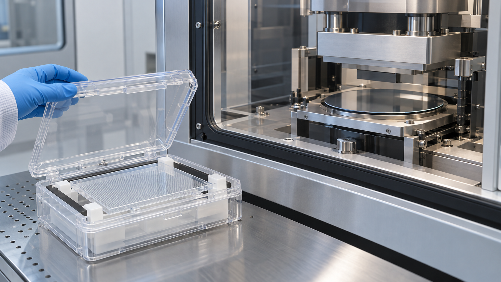
Nanoscale patterns are not made by projecting light alone. Nanoimprint lithography presses a mold into a resist and copies its shape, and directed self-assembly (DSA) lets block copolymers arrange themselves. In both, something other than the wavelength of light sets the feature size. What changes is where the difficulty sits: template defects, overlay and materials design. This explainer draws on official material from Canon, Dai Nippon Printing (DNP), Kioxia and imec, the IEEE IRDS roadmap and peer-reviewed papers to lay out the principles, the defect and overlay issues, and where memory-oriented adoption stands today.
- Top-down and bottom-up: the short version
- How nanoimprint works: thermal and UV
- How the template is made
- Our calculation: what “defects per cm²” means on a wafer
- A materials engineer's view (1): the difficulty gathers at the contact surface
- Overlay accuracy: how to read the numbers
- Directed self-assembly: polymers that arrange themselves
- A materials engineer's view (2): block copolymer design is a tug-of-war between χ and N
- Where memory-oriented adoption stands, as far as official sources show
- What is still hard, and what could not be confirmed
- Glossary / References / Claim-to-source audit
Sourced = stated in published material (link given)
Our calculation = a figure this article derived, with the assumptions spelled out
Not yet confirmed = a plan or a target with no confirmed track record
Structural readings and materials-design interpretations are marked separately as Commentary, and weakly supported ideas as Inference.
Performance figures are each company's own statements (manufacturer's stated values). Numbers measured under different conditions are not ranked against each other.
1. Top-down and bottom-up: the short version
The mainstream way to make circuit patterns is photolithography, which projects a reduced image of a master pattern onto the wafer with light. imec calls this “traditional top-down” patterning and presents DSA, which uses the phase separation of polymers, as a “bottom-up” route that can complement or extend it Sourced. ISO/TS 80004-8:2020, the vocabulary standard for nanomanufacturing processes, likewise says in its introduction that nanomanufacturing includes both bottom-up directed assembly and top-down high-resolution processing Sourced [Reference 29]. The two methods in this article can be summarised as follows (our commentary).
- Nanoimprint lithography (NIL): a mold (template) is pressed into resist and its shape is copied. The template's own dimensions set the feature size. Because the transfer does not pass through an optical system, Canon says fine patterns on the mask are reproduced faithfully Sourced
- Directed self-assembly (DSA): a block copolymer, two polymers joined end to end, forms stripes or hole arrays on its own when heated. Chain length and the incompatibility of the blocks set the feature size. A guide that fixes orientation and position still has to be made separately, for example by photolithography Sourced
- What they share: both avoid the limits of light, and in exchange the main issues become how defects arise, overlay, and material uniformity (our commentary)
2. How nanoimprint works: thermal and UV
Nanoimprint was proposed in the 1990s. In 1995 Chou and co-workers reported pressing a mold into a thin thermoplastic polymer film to make vias and trenches as small as 25 nm, 100 nm deep Sourced. They noted that the printable size was limited by the size of the mold Sourced. In 1996 the same group described compression molding that creates a thickness contrast in a resist film, followed by anisotropic etching to cut through the thin regions Sourced. Those thin regions are the residual layer discussed below.
Today's semiconductor tools are mainly UV-curable. A paper on NIL tool performance by Shudo et al. (Photomask Japan 2024) describes the process as follows Sourced.
- A low-viscosity resist is jetted onto the substrate where needed, one shot (field) at a time
- The patterned template is lowered, and the resist flows into its relief by capillary action
- UV light crosslinks (cures) the resist and the template is pulled away
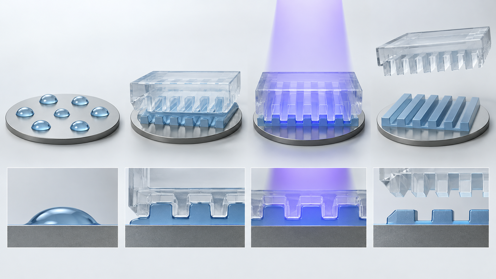
Shapes, colors and dimensions are illustrative. Consult the original schematic below for exact values and label correspondence.
View the original SVG schematic and exact annotations
Reading guide and original schematic labels: The UV nanoimprint sequence (conceptual cross-section) / Grey = substrate / blue = resist / brown = template / yellow = UV / 1. Dispense / 2. Press and fill / 3. UV cure / 4. Separate / Residual layer (thin film left) / Resist is dropped only / where it is needed / Capillary action fills / the relief (filling) / UV crosslinks and / hardens the resist / The relief stays / in the resin / Dispense, capillary filling, UV crosslinking and separation follow Shudo et al. (2024) [Ref. 15] and Kioxia [Ref. 13]. / No dimensions or thicknesses are shown. Residual layer: Chou et al. (1996) [Ref. 20]; the etch step after it is this article's reading.
| Item | Thermal nanoimprint | UV nanoimprint |
|---|---|---|
| Resist | Thin thermoplastic polymer film (Chou et al., 1995) | Low-viscosity photo-curable resist, dropped locally (Shudo et al., 2024) |
| How it hardens | Commentary: the polymer is softened, pressed, then cooled to set, so a temperature cycle is needed | UV crosslinking (Shudo et al., 2024). UV must reach the resist through the template or the substrate (our commentary) |
| Tools for semiconductor manufacturing | Not found in the official sources used here | Canon's FPA-1200NZ2C and similar (inkjet dispensing plus UV) [References 1, 2] |
The thermal entry in “How it hardens” is commentary drawn from the nature of thermoplastics, not a statement from a source. Production tools for thermal nanoimprint could not be confirmed in official material.
For its UV tool, Canon explains that the transfer does not go through an optical system, so fine mask patterns are reproduced faithfully, and that complex two- or three-dimensional patterns can be formed in a single imprint, which may reduce the cost of ownership (CoO) Sourced. Resist is applied only where needed, so there is no wasted material (Ifuku et al., 2024) Sourced. The product page lists a 6-inch mask, a 300 mm wafer, a 26 × 33 mm field and overlay accuracy of 4 nm or better Sourced (manufacturer's stated value; the page does not say how overlay was measured or which statistic it is. Section 6 returns to this).
3. How the template is made
In nanoimprint the template is the master and the dimensional reference itself. Kioxia explains that, unlike photolithography, the resist pattern on the wafer has the same scale as the master pattern on the template, and that template patterns, originally written by electron-beam lithography, can be formed at dimensions in the 10 nm range Sourced. In reduction-projection photolithography the master is drawn at enlarged dimensions (our commentary). So nanoimprint asks the master to be as fine as the pattern on the wafer.
| What was published | Source and conditions |
|---|---|
| A 14 nm half-pitch template made with a self-aligned sidewall process, and a 14 nm half-pitch resist pattern formed on a wafer | Kioxia Advanced Technology Research Laboratories (posted 17 March 2020), presented at SPIE Advanced Lithography 2019 [Reference 11] |
| A template with 10 nm line width, made by applying SADP (self-aligned double patterning) to a pattern written with an electron-beam mask writer | DNP news release, 9 December 2025. DNP describes it as suited to 1.4 nm-generation logic (company statement) [Reference 9] |
| For sub-15 nm templates, direct writing in resist lacks resolution and sensitivity, so SADP is applied. Template defect density has not yet reached a volume-manufacturing level; the target is below 1 defect/cm² | Motokawa et al. (Photomask Technology 2020), a joint study with the University of Hyogo and Kioxia [Reference 17] |
| Programmed defects in a 19 nm L/S template were repaired using multiple patterning, from edge bumps up to 45 nm in size. Below 20 nm, conventional electron-beam repair is limited in resolution, yield and turnaround time | Nagai et al. (Photomask Technology 2024). Evaluated on programmed defects [Reference 18] |
All Sourced. The measurements and conditions differ, so the numbers cannot be ranked against each other. DNP has begun evaluation and aims to start volume production in 2027 Not yet confirmed.
Motokawa et al. say that sub-15 nm templates are hard to make by direct writing in resist alone, so they use methods like SADP, which doubles line density through film deposition and etching Sourced. DNP uses the same SADP Sourced. Nanoimprint is a way to pattern without light, but on the master side, deposition, etching and electron-beam writing are all brought to bear (our commentary).
4. Our calculation: what “defects per cm²” means on a wafer
Two kinds of defect numbers appear in the public literature on nanoimprint. One is from Iwasaki et al. (2022): after process optimisation, a multi-module NZ2C system with four imprint heads is expected to reach a throughput of 124 wafers per hour and a defectivity of 0.005 defects/cm² Sourced. That paper presents it as an expectation after optimisation, not a measurement, and for a spin-coating variant (SC-FIL, which spin-coats the resist) rather than the inkjet-dispense method. The other is a research goal from Motokawa et al. (2020): bringing the defect density of sub-15 nm templates below 1 defect/cm² Sourced.
Let us convert “per cm²” into physical sizes Our calculation.
- Area of a 300 mm wafer: π × (15 cm)² = about 707 cm² (whole wafer; the usable area is smaller)
- Area of one field: Canon's stated field size of 26 × 33 mm = 2.6 × 3.3 = about 8.58 cm²
- At 0.005 defects/cm²: 707 × 0.005 = about 3.5 per wafer; 8.58 × 0.005 = about 0.04 per field
- At 1 defect/cm²: 707 × 1 = about 707 per wafer; 8.58 × 1 = about 8.6 per field
Assumptions and limits: this is a simple conversion that assumes defects are spread evenly over the area. The two numbers are different quantities. 0.005 defects/cm² is an expected density of pattern defects on the wafer, while “below 1 defect/cm²” is a research goal for the template itself; they are not to be compared on the same basis. Whether either meets what customers require in volume production could not be confirmed from the public material used here. Ifuku et al. add that logic often needs defect levels well below those of memory, which can use redundancy Sourced.
5. A materials engineer's view (1): the difficulty gathers at the contact surface
Photolithography defines the shape with light, without touching the resist. In nanoimprint the template, the resist and the wafer make physical contact, so materials and interfaces come to the front. The public material shows the following.
- The resist requirements pull against each other: Kioxia reports that etching favors a thick resist, yet a thick resist makes defects more likely in the NIL step, so the two are hard to reconcile. It used a resist with high etch resistance and optimised the template structure, NIL conditions and etch conditions, and obtained a three-dimensional dual-damascene profile of L/S = 4X/4X nm across the whole wafer Sourced [Reference 13]
- Filling is a race against time: Iwasaki et al. assumed Washburn's model of capillary flow, identified a defect-generation mechanism specific to SC-FIL, and optimised the process for throughput and low defect density Sourced. Kioxia reports shorter resist-filling time and higher throughput using materials that help bubbles escape (resist material and a gas-permeable spin-on carbon) Sourced [Reference 11]. Canon says it introduced a resist that shortens imprint time Sourced [Reference 6]
- Particles can destroy the template: Canon explains that a particle trapped between template and wafer can cause not only device defects but also destruction of the template pattern itself, which is why particle control is extremely important Sourced [Reference 3]. Kioxia reports longer template life through particle-removal technology Sourced [Reference 11]
- Separation must not deform the pattern: Canon says it developed nanometer-level control so that the raised resist patterns do not deform when the template is removed Sourced [Reference 3]
What a materials engineer can read from this is that the resist has to satisfy several conditions at once: low viscosity (fast filling), strength after curing (etch resistance), clean release from the template, and few defects (thickness, gas) (our commentary). Specific materials or methods for the template surface treatment that aids release could not be confirmed in the official sources used here.
There is also the residual layer. As Chou et al. (1996) show, the thin parts of the relief formed by pressing must be removed by anisotropic etching, so the uniformity of residual-layer thickness feeds straight into dimensional accuracy downstream (our commentary). Kioxia's attention to etch resistance, CD shift and etch-mask consumption reads as part of this chain.
6. Overlay accuracy: how to read the numbers
A chip is built from dozens of layers, so how accurately each new pattern can be aligned to the layers beneath (overlay) is decisive. In nanoimprint the template physically touches the wafer, which makes alignment particularly demanding. Canon explains that it measures template-to-wafer misalignment in real time with moire patterns, and developed its own approach that thermally deforms the wafer with a laser to match the lower layer Sourced. Wafer thermal deformation has conventionally been treated as something that degrades alignment; Canon says it takes the opposite view and uses it. Kioxia reports better overlay from a technique that corrects complex higher-order distortion Sourced.
| Value | Source | What it is (conditions and level) |
|---|---|---|
| 4 nm or better | Canon product page, FPA-1200NZ2C [Reference 2] | “Overlay Accuracy”. A manufacturer's stated specification. No measurement method or statistic (3σ, maximum and so on) is given |
| 2 nm | Kioxia (October 2022) [Reference 10] | Described as an alignment accuracy to the substrate that NIL has achieved. Detailed conditions are not given (a page introducing the company's research presentation) |
| Under 3 nm | Kioxia (October 2022) [Reference 10] | For a 14 nm half-pitch template with separately formed alignment marks, alignment error to a silicon substrate under 3 nm. A laboratory evaluation |
| 3.9 nm (X) / 3.4 nm (Y) | Iwasaki et al. (2022) [Reference 14] | Mix-and-match overlay accuracy (3σ), presumably against layers made another way (our commentary). A laboratory evaluation |
| 2.1 to 2.8 nm | Shudo et al. (2024); Ifuku et al. (2024) [References 15, 16] | The overlay error budget for critical DRAM layers, 15 to 20% of the minimum half-pitch; the value for 14 nm |
All Sourced. Measurement methods, statistics, layers and tools differ, so these numbers cannot be ranked against each other. The last row is an example of a requirement, not an achieved value.
On size alone, Canon's stated figure (4 nm or better) looks larger than the budget for critical 14 nm half-pitch DRAM layers (2.1 to 2.8 nm) Our calculation (14 × 0.15 = 2.1; 14 × 0.20 = 2.8). But the statistic and conditions behind the stated figure are not published, so whether the comparison is even valid cannot be judged. Ifuku et al. add that putting a new lithography into production needs more than overlay, defect levels and throughput: it needs an ecosystem around the tool, such as drop-pattern generation, NIL process simulation, virtual metrology and pattern-transfer techniques Sourced.
7. Directed self-assembly: polymers that arrange themselves
The self-assembly under discussion for semiconductors is the microphase separation of block copolymers (BCPs). imec explains that DSA defines a pattern by the microphase separation of a block copolymer, and that the pattern can be engineered through the polymer's composition and size Sourced. The two polymers (blocks) resist mixing, but because they are chained together they cannot separate on a large scale. The result is a stripe or hole array with a period of a few to a few tens of nanometers, set by chain length (our commentary; the theory goes back to Leibler, 1980, and Bates et al., 2014 is a review of lithographic use).
Left alone, though, orientation and position come out random. A guide (a prepattern) that directs the assembly is what makes it “directed” self-assembly. imec explains that the guide can be lines and spaces or holes, and the resulting pattern has a far finer period (30 to 5 nm) than the guide Sourced. In 2008 Ruiz et al. reported defect-free arrays on chemically patterned surfaces with density multiplied by four and size halved, at densities up to 1 terabit per square inch Sourced. They note that the thermodynamic driving forces are small, so low-energy defects are easily trapped in block copolymers Sourced.
| Generation | What was published | Source and conditions |
|---|---|---|
| PS-b-PMMA (first generation) | In 2019, line/space patterns at 28 nm pitch with low and stable levels of bridges and dislocations | imec news release (25 February 2021) [Reference 21]. Suh et al. (2021) say L/S patterns around 30 nm pitch have been demonstrated, and that the main challenge is controlling DSA-specific defects within a time acceptable for volume manufacturing [Reference 24] |
| High-χ block copolymer (second generation) | Line/space patterns at 18 nm pitch. After 60 seconds of self-assembly, no dislocations were detected in the best case | imec (February 2021). From a guide with a 90 nm period made by ArF immersion lithography, on a volume-manufacturing-compatible track. Materials partners: Merck KGaA, Brewer Science, Nissan Chemical and Tokyo Ohka Kogyo [Reference 21] |
All Sourced. “No dislocations detected” is a statement about the best case, not an average defect density. The stage described is transferring the pattern to the underlayer to continue defect inspection.
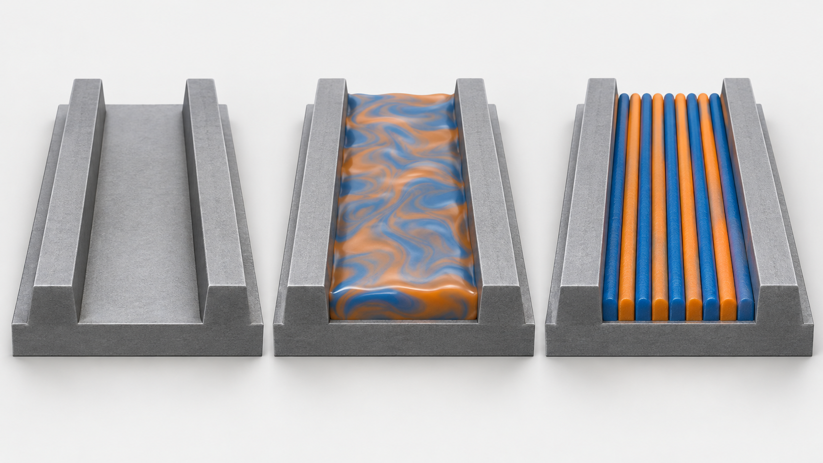
Shapes, colors and dimensions are illustrative. Consult the original schematic below for exact values and label correspondence.
View the original SVG schematic and exact annotations
Reading guide and original schematic labels: DSA: between the guides, the polymer forms fine stripes by itself (top view) / Grey = guide / blue and orange = the two blocks of the block copolymer / 1. Make the guide / 2. Coat the polymer / 3. Heat: phase separation / A coarse-period guide is / made by photolithography etc. / A film in which the two / blocks are mixed / Fine stripes line up / regularly between the guides / imec example: 90 nm period / imec example: 18 nm pitch / 4. One block is removed and the other serves as an etch mask to transfer the pattern (as imec describes) / Getting 18 nm-pitch stripes from a 90 nm-period guide is an imec result [Reference 21]. / The number of stripes and the grain size are simplified; this is not an actual arrangement or defect.
In imec's example, a guide with a 90 nm period gave stripes at 18 nm pitch. 90 ÷ 18 = 5. Within one guide period there fit five periods of the 18 nm-pitch pattern (five stripes of each of block A and block B, ten in all) Our calculation. Photolithography only has to make the coarse guide; the fine period is made by the molecules. That is the idea behind “density multiplication” (our commentary).
8. A materials engineer's view (2): block copolymer design is a tug-of-war between χ and N
The period of a block copolymer is set mostly by chain length (degree of polymerisation, N). To shrink the period you reduce N, but keeping the blocks phase-separated needs the product of their incompatibility (χ) and N to stay above a threshold (Leibler's theory; our commentary). If N goes down, χ has to go up, and that is why “high-χ” materials are needed. imec says the same: the process can be scaled to smaller pitches by gradually raising χ Sourced.
Three points deserve a materials engineer's attention.
- The defects are of a different nature: in photolithography, imec says, stochastic printing failures and line-edge roughness that come from the reaction of photosensitive material with light are the issue Sourced. DSA defects, in the framing of Suh et al., arise from the block copolymer not assembling ideally Sourced. Ruiz et al. say the small thermodynamic driving force lets low-energy defects get trapped Sourced. So the trade-off is how long you allow the film to approach equilibrium versus throughput (our commentary)
- Getting the pattern out is hard: imec calls the transfer of 18 nm-pitch stripes into the underlayer “very challenging”: one block was etched away selectively, and the remaining block served as a mask to pattern a SiN layer Sourced. Laib et al. add that for volume manufacturing critical dimensions, line roughness and defectivity all have to be met by dry etch, and that these are the current obstacles Sourced. Securing etch selectivity between the two blocks while raising χ reads as a materials-design trade-off (our commentary)
- Orientation control (inference): high-χ pairs often differ strongly in surface energy as well, which can make each block segregate to the substrate or air interface and make it hard to stand the stripes perpendicular to the substrate Inference. The official material used here did not give a concrete method for orientation control of high-χ materials
In short, DSA materials development is molecular design that must deliver fine (high χ), defect-free (reaching equilibrium quickly) and extractable (etch selectivity) at once, plus the synthesis, purification and uniformity that go with it. That imec works with four materials suppliers (Merck KGaA, Brewer Science, Nissan Chemical, Tokyo Ohka Kogyo), a track-tool maker (SCREEN) and an etch partner (Tokyo Electron) as one ecosystem is a sign of this Sourced.
9. Where memory-oriented adoption stands, as far as official sources show
(1) Nanoimprint
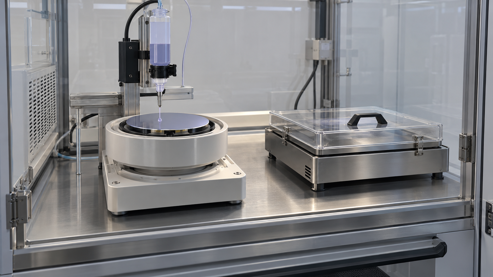
In its July 2017 announcement Canon had supplied a tool to Toshiba Memory's (now Kioxia's) Yokkaichi plant, as a step toward volume production Sourced. Canon then launched the FPA-1200NZ2C in October 2023 Sourced and in September 2024 shipped one to the US semiconductor consortium TIE for R&D and prototyping Sourced. What its 2026 earnings briefings say is shown in the figure and table below.
| Date | What was published |
|---|---|
| 20 July 2017 | Canon supplies the FPA-1200NZ2C to Toshiba Memory's Yokkaichi plant, which it describes as progress toward what would be the world's first memory volume production using NIL [Reference 5] |
| 13 October 2023 | FPA-1200NZ2C launched. Minimum line width 14 nm (equivalent to the 5 nm node, in Canon's words); with mask improvements 10 nm (2 nm node) is expected [Reference 1] |
| 26 September 2024 | Shipped to TIE in the US for “research and development of advanced semiconductors and production of prototypes” [Reference 4] |
| 7 March 2025 | In a business briefing Canon says it will accelerate partnerships with several major customers and promote installation and process verification at customer sites to realise volume production for advanced devices [Reference 6] |
| 9 December 2025 | DNP announces a 10 nm-line NIL template. It has begun evaluation and aims to start volume production in 2027; its sales target for NIL is 4 billion yen in fiscal 2030 [Reference 9] Not yet confirmed |
| 23 April 2026 | Canon earnings briefing: systems delivered to a major semiconductor manufacturer passed basic performance verification and entered an evaluation and validation phase that simulates actual production; progress toward mass-production adoption in 2027 is described as steady [Reference 7] Not yet confirmed |
| 27 July 2026 | Canon earnings briefing: additional systems shipped in June to customers evaluating and verifying; working toward mass-production adoption in 2027, Canon has entered a production-validation phase using customer wafers under conditions that simulate actual manufacturing lines, with multiple customers advancing validation [Reference 8] Not yet confirmed |
The earlier rows are Sourced (announcements, specifications); the 2027 volume adoption and volume production are each company's targets and are Not yet confirmed. Customer names and the target device (NAND, DRAM or logic) do not appear in the cited passages of the 2026 briefings.
Canon and DNP both say power consumption is about one-tenth of photolithography: Canon in comparison with exposure technology for advanced logic Sourced [Reference 3], DNP in comparison with ArF immersion and EUV Sourced [Reference 9]. Both are each company's own claims, and we could not confirm independent verification. Canon's article records that Canon, DNP and Kioxia received an environmental award in 2022 for their NIL work Sourced [Reference 3], but we found no official statement from Kioxia that it has begun using NIL in NAND volume production.
(2) Directed self-assembly (DSA)
The lithography chapter of the 2023 IRDS roadmap says DSA is being evaluated or used for device manufacturing in logic, memory and CMOS sensors, and that it is used to make repeated, smooth, fine-pitch patterns from rough initial patterns at reasonable cost of ownership Sourced. One concrete example it points to is an image sensor: a back-illuminated CMOS image sensor with a “pseudo high-refractive-index film” made of an array of minute holes formed by DSA, with enhanced sensitivity at 400 to 550 nm. The paper calls it the first report of an image sensor fabricated using the DSA process (Oshiyama et al., 2021) Sourced. In 2021, meanwhile, imec positioned DSA as a way to complement traditional top-down patterning, pointing to potential for sub-2 nm nodes and no more Sourced.
Within the scope of this article we could not find a company document stating that DSA is used for a main layer in logic or memory volume production. When, in which layer and at which company DSA becomes practical cannot be decided from the primary sources today.
10. What is still hard, and what could not be confirmed
(1) Template defects, lifetime and repair
In 2020, the defect density of sub-15 nm templates was reported as not yet at a volume-manufacturing level Sourced [Reference 17]. Repairing templates below 20 nm is limited by resolution, yield and turnaround time with conventional electron-beam repair Sourced [Reference 18]. Because the template is worn by contact, template lifetime and replacement cost shape the economics of volume production. However, concrete figures for template lifetime or number of wafers per template could not be confirmed in the official sources used here.
(2) Actual overlay and defect performance
The statistic and measurement conditions behind Canon's stated overlay (4 nm or better) are not published, so its relation to the DRAM critical-layer budget (2.1 to 2.8 nm) cannot be judged. For throughput (wafers per hour), apart from the expectation of Iwasaki et al. (124 wafers per hour, four heads), no official stated value for a production tool could be confirmed.
(3) Timing of volume adoption
Canon says it aims for volume adoption in 2027, but customer names, target devices and layers have not been published Not yet confirmed. DNP's start of template production (2027) is also a target.
(4) DSA defects and materials
For DSA, defect control, etch transfer and orientation control for high-χ materials are named as challenges Sourced [References 21, 24, 25]. IRDS says DSA is being evaluated or used, but does not say which company uses it in which device.
- Nanoimprint is a method in which the template sets the feature size, and the difficulty gathers in the template, resist, particles, release and overlay. Canon's stated figures are a minimum line width of 14 nm and overlay of 4 nm or better Sourced (manufacturer's stated values)
- Making the template calls on a whole other set of fine-patterning tools. A 10 nm-line template is made with electron-beam writing and SADP Sourced
- Converted from “per cm²”, 0.005 defects/cm² is about 3.5 on a whole 300 mm wafer and 1 defect/cm² is about 707 Our calculation. The two are different quantities
- DSA lets polymers arrange themselves; imec showed 18 nm pitch with a high-χ material. The difficulty lies in defect control and etch transfer Sourced
- Where adoption stands: nanoimprint is in production-like validation at customers, and Canon aims for volume adoption in 2027 Not yet confirmed. DSA is described as evaluated or used, but we found no named volume-production example
11. Glossary
- Nanoimprint lithography (NIL)
- A fine-patterning technique that presses a patterned template into resist and copies its shape.
- Template (mold, mask)
- The master for nanoimprint. It carries a pattern of the same size as on the wafer.
- Residual layer
- The thin resist film left at the bottom of recesses after pressing. It is removed afterwards by etching.
- Separation (release)
- Pulling the template away from the cured resin.
- Capillary action
- Liquid flowing into narrow gaps on its own. It fills the template recesses.
- Overlay
- How accurately a new layer's pattern is aligned to the pattern beneath.
- Mix-and-match
- Using layers made with different exposure methods or tools in one device.
- SADP
- Self-aligned double patterning. Doubles line density through film deposition and etching.
- DSA
- Directed self-assembly. A guide directs orientation and position of an arranging block copolymer.
- Block copolymer (BCP)
- A polymer in which chains of two or more polymers are joined end to end.
- Microphase separation
- Blocks that resist mixing, chained together, separate into domains a few to a few tens of nm across.
- χ (chi)
- The interaction parameter that expresses how poorly two components mix.
- PS-b-PMMA
- A block copolymer of polystyrene and poly(methyl methacrylate). The most widely used material in DSA to date.
- EUV
- Extreme ultraviolet. The short-wavelength light used in leading-edge photolithography.
- CoO
- Cost of ownership. The total cost of owning and operating a tool.
12. References (primary sources)
- Canon news release, "Nanoimprint lithography semiconductor manufacturing system that covers diverse applications with simple patterning mechanism", 13 October 2023 — global.canon
- Canon product page, "FPA-1200NZ2C" (specifications) — global.canon
- Canon technology article, "Nanoimprint Lithography", 14 September 2023 — global.canon
- Canon news release, "Canon delivers FPA-1200NZ2C nanoimprint lithography system for semiconductor manufacturing to the Texas Institute for Electronics", 26 September 2024 — global.canon
- Canon news release, "Canon provides nanoimprint lithography manufacturing equipment to Toshiba Memory's Yokkaichi Operations plant", 20 July 2017 — global.canon
- Canon business briefing materials, 7 March 2025 (PDF) — global.canon
- Canon First Quarter 2026 Results, 23 April 2026, with briefing transcript (PDF) — global.canon
- Canon Second Quarter 2026 Results, 27 July 2026, with briefing transcript (PDF) — global.canon
- Dai Nippon Printing (DNP), "DNP Achieves 10nm Line-pattern resolution on Nanoimprint Template for Cutting-Edge Semiconductors", 9 December 2025 — global.dnp
- Kioxia advanced technology topic, "Evaluation of alignment accuracy for nanoimprint lithography" (in Japanese), 5 October 2022 — kioxia.com
- Kioxia advanced technology topic, "Development of half-pitch 14 nm one-shot patterning with nanoimprint lithography" (in Japanese), 17 March 2020 — kioxia.com
- Kioxia advanced technology topic, "Co-optimization of design and process for higher nanoimprint lithography productivity" (in Japanese), 5 October 2022 — kioxia.com
- Kioxia advanced technology topic, "Dual-damascene structure formation using nanoimprint lithography and dry etching" (in Japanese), 26 April 2023 — kioxia.com
- Iwasaki et al., "Improvement of productivity by spin-coating and flash imprint lithography", J. Micro/Nanopattern. Mater. Metrol. 21(1), 011008 (2022) — doi.org
- Shudo et al., "Nanoimprint performance improvements for high volume semiconductor device manufacturing", Photomask Japan 2024, Proc. SPIE 13177 — doi.org
- Ifuku et al., "Nanoimprint lithography performance advances for new application spaces", Novel Patterning Technologies 2024, Proc. SPIE 12956 — doi.org
- Motokawa et al., "Resist pattern inspection for defect reduction in sub-15 nm templates", Photomask Technology 2020, Proc. SPIE 11518 — doi.org
- Nagai et al., "Development of repairing technology for nanoimprint templates by multiple patterning technology", Photomask Technology 2024, Proc. SPIE 13216 — doi.org
- Chou, Krauss and Renstrom, "Imprint of sub-25 nm vias and trenches in polymers", Appl. Phys. Lett. 67, 3114 (1995) — doi.org
- Chou, Krauss and Renstrom, "Imprint Lithography with 25-Nanometer Resolution", Science 272, 85 (1996) — doi.org
- imec, "Imec Demonstrates 18nm Pitch Line/Space Patterning With a High-Chi Directed Self-Assembly Process", 25 February 2021 — imec-int.com
- IEEE IRDS, "International Roadmap for Devices and Systems 2023: Lithography" (PDF) — irds.ieee.org
- Ruiz et al., "Density Multiplication and Improved Lithography by Directed Block Copolymer Assembly", Science 321, 936 (2008) — doi.org
- Suh et al., "Development of high-chi directed self-assembly process based on key learning from PS-b-PMMA system", Proc. SPIE 11612 (2021) — doi.org
- Laib et al., "Etch developments in response to DSA challenges", Proc. SPIE 11610 (2021) — doi.org
- Oshiyama et al., "Visible Light Sensitivity Enhancement of CMOS Image Sensor with Pseudo High Refractive Index Film Integrated by Directed Self-Assembly Process", IEEE EDTM 2021 — doi.org
- Leibler, "Theory of Microphase Separation in Block Copolymers", Macromolecules 13, 1602 (1980) — doi.org
- Bates et al., "Block Copolymer Lithography", Macromolecules 47, 2 (2014) (a review; only the title and bibliographic details were checked for this article) — doi.org
- ISO, ISO/TS 80004-8:2020 "Nanotechnologies — Vocabulary — Part 8: Nanomanufacturing processes" (table of contents and introduction in the public preview were checked) — committee.iso.org
13. Claim-to-source audit
| Claim in the text | Basis | Label |
|---|---|---|
| That imec calls photolithography “traditional top-down” and DSA a bottom-up complement or alternative; that DSA defines the pattern by microphase separation of a block copolymer, engineerable through composition and size; that the guide is lines/spaces or holes and gives periods of 30 to 5 nm; 28 nm pitch with PS-b-PMMA in 2019; 18 nm pitch with a high-χ BCP in 2021 (90 nm-period guide, ArF immersion, 60 seconds, no dislocations in the best case); the materials partners; and that etch transfer was very challenging | Reference 21 https://www.imec-int.com/en/press/imec-demonstrates-18nm-pitch-linespace-patterning-high-chi-directed-self-assembly-process | Sourced |
| Canon: transfer without an optical system reproduces fine mask patterns faithfully; complex 2D and 3D patterns in a single imprint; minimum line width of 14 nm (5 nm node equivalent) and 10 nm (2 nm node) expected with mask improvements; environment control to suppress particles; launch on 13 October 2023 | Reference 1 https://global.canon/en/news/2023/20231013.html | Sourced |
| FPA-1200NZ2C specifications: field 26 × 33 mm, 6-inch mask, 300 mm wafer, overlay accuracy of 4 nm or better (no measurement method or statistic given) | Reference 2 https://global.canon/en/product/indtech/semicon/fpa1200nz2c.html | Sourced |
| Canon technology article: control of resist amount and position; control so raised patterns do not deform at release; real-time misalignment measurement by moire; wafer thermal deformation by laser to match the lower layer; particles can destroy the template; power consumption about one-tenth of exposure technology for advanced logic; the 2022 environmental award | Reference 3 https://global.canon/en/technology/nil-2023.html | Sourced |
| Shipment to TIE on 26 September 2024 for R&D and prototyping; supply to Toshiba Memory's Yokkaichi plant on 20 July 2017 described as progress toward the world's first memory volume production using NIL | Reference 4 https://global.canon/en/news/2024/20240926.html Reference 5 https://global.canon/en/news/2017/20170720.html | Sourced |
| Canon business briefing (7 March 2025): accelerating partnerships with several major customers, installation and process verification at customer sites, introduction of a resist that shortens imprint time | Reference 6 https://global.canon/en/ir/conference/pdf/housin2025ind-e.pdf | Sourced |
| 23 April 2026: systems delivered to a major semiconductor manufacturer passed basic performance verification and entered a validation phase simulating actual production. 27 July 2026: additional shipments in June; production-validation phase on customer wafers under simulated line conditions; multiple customers validating. Mass-production adoption in 2027 as the aim | Reference 7 https://global.canon/en/ir/conference/pdf/conf2026q1e-note.pdf Reference 8 https://global.canon/en/ir/conference/pdf/conf2026q2e-note.pdf | Not yet confirmed |
| DNP: a template with 10 nm line width (electron-beam mask writer plus SADP); 1.4 nm-generation equivalence (company statement); power about one-tenth of ArF immersion and EUV (company claim); evaluation begun and volume production aimed for in 2027; NIL sales target of 4 billion yen in fiscal 2030 | Reference 9 https://www.global.dnp/news/detail/20177718_4126.html | Not yet confirmed |
| Kioxia: template patterns written by electron-beam lithography can reach the 10 nm range; alignment accuracy of 2 nm described as achieved; for a 14 nm half-pitch template, alignment marks formed separately gave alignment error under 3 nm | Reference 10 https://www.kioxia.com/ja-jp/rd/technology/topics/topics-31.html | Sourced |
| Kioxia: a 14 nm half-pitch template by a self-aligned sidewall process; longer template life through particle removal; shorter filling time with a gas-permeable spin-on carbon that helps bubbles escape; better overlay by correcting higher-order distortion | Reference 11 https://www.kioxia.com/ja-jp/rd/technology/topics/topics-13.html | Sourced |
| Kioxia: design constraints for NIL alignment marks and a rule combining layout coverage and substrate step height, aimed at better yield | Reference 12 https://www.kioxia.com/ja-jp/rd/technology/topics/topics-32.html | Sourced |
| Kioxia: etching favors thick resist, but thick resist makes NIL defects likely and the two are hard to reconcile; a resist with high etch resistance and optimised conditions gave an L/S = 4X/4X nm 3D dual-damascene profile across the whole wafer | Reference 13 https://www.kioxia.com/ja-jp/rd/technology/topics/topics-42.html | Sourced |
| Iwasaki et al.: whole 300 mm wafer imprinted by SC-FIL (spin-coating and flash imprint); 26 nm half-pitch lines; mix-and-match overlay (3σ) of 3.9 nm (X) and 3.4 nm (Y); defect mechanism identified with Washburn's model; a four-head NZ2C system is expected to reach 124 wafers per hour and 0.005 defects/cm² | Reference 14 https://doi.org/10.1117/1.JMM.21.1.011008 | Sourced |
| Shudo et al. and Ifuku et al.: inkjet dispense, template lowered, capillary fill, UV crosslinking, separation; overlay budget for critical DRAM layers of 15 to 20% of the minimum half-pitch, 2.1 to 2.8 nm for 14 nm; logic needs lower defect levels than memory; the need for an ecosystem (drop-pattern generation, process simulation, virtual metrology); resist applied only where needed | Reference 15 https://doi.org/10.1117/12.3034104 Reference 16 https://doi.org/10.1117/12.3012070 | Sourced |
| Motokawa et al.: direct writing in resist lacks resolution and sensitivity for sub-15 nm templates, so SADP is applied; template defect density is below a volume-manufacturing level and the goal is under 1 defect/cm² | Reference 17 https://doi.org/10.1117/12.2572389 | Sourced |
| Nagai et al.: below 20 nm, conventional electron-beam repair is limited in resolution, yield and turnaround time; programmed defects in a 19 nm L/S template were repaired from edge bumps up to 45 nm in size | Reference 18 https://doi.org/10.1117/12.3034660 | Sourced |
| Chou et al. (1995): a mold pressed into a thin thermoplastic polymer film made vias and trenches down to 25 nm and 100 nm deep; the printable size is limited by the mold | Reference 19 https://doi.org/10.1063/1.114851 | Sourced |
| Chou et al. (1996): compression molding creates a thickness contrast and anisotropic etching cuts through it; 25 nm metal features at a 70 nm period | Reference 20 https://doi.org/10.1126/science.272.5258.85 | Sourced |
| IRDS 2023: DSA is being evaluated or used for device manufacturing in logic, memory and CMOS sensors; used to make repeated smooth fine-pitch patterns from rough initial patterns at reasonable cost of ownership | Reference 22 https://irds.ieee.org/images/files/pdf/2023/2023IRDS_Litho.pdf | Sourced |
| Ruiz et al. (2008): defect-free arrays on chemically patterned surfaces with density multiplied by four, size halved, up to 1 terabit per square inch; small thermodynamic driving forces let low-energy defects be trapped | Reference 23 https://doi.org/10.1126/science.1157626 | Sourced |
| Suh et al. (2021): L/S patterns around 30 nm pitch demonstrated with PS-b-PMMA; the challenge is controlling DSA-specific defects within a time acceptable for volume manufacturing. Laib et al. (2021): volume manufacturing needs critical dimensions, line roughness and defectivity all met by dry etch | Reference 24 https://doi.org/10.1117/12.2585169 Reference 25 https://doi.org/10.1117/12.2584944 | Sourced |
| Oshiyama et al. (2021): a back-illuminated CMOS image sensor with a pseudo high-refractive-index film of minute holes made by DSA, with enhanced sensitivity at 400 to 550 nm; called the first report of an image sensor made with DSA | Reference 26 https://doi.org/10.1109/EDTM50988.2021.9420898 | Sourced |
| That the introduction to ISO/TS 80004-8:2020, the vocabulary standard for nanomanufacturing processes, says nanomanufacturing includes both bottom-up directed assembly and top-down high-resolution processing | Reference 29 https://committee.iso.org/standard/74666.html | Sourced |
| The theory of microphase separation in block copolymers (Leibler, 1980) and a review of block copolymer lithography (Bates et al., 2014; only the title and bibliographic details were checked for this article) | Reference 27 https://doi.org/10.1021/ma60078a047 Reference 28 https://doi.org/10.1021/ma401762n | Sourced |
| The area of a 300 mm wafer as about 707 cm² (pi × 15²) and of one field as about 8.58 cm² (2.6 × 3.3); 0.005 defects/cm² as about 3.5 per wafer and about 0.04 per field; 1 defect/cm² as about 707 per wafer and about 8.6 per field; the check of 15% and 20% of 14 nm (2.1 and 2.8 nm); 90 ÷ 18 = 5 | Our calculation. It assumes defects are spread evenly over the area. 0.005 defects/cm² (an expected value for defects on the wafer) and below 1 defect/cm² (a template goal) are different quantities and are not compared on the same basis | Our calculation |
| Canon's aim of volume adoption in 2027, and DNP's aim to start volume production of templates in 2027 | Company targets and plans, not results (an outlook). Customer names, target devices and layers could not be confirmed in the published material | Not yet confirmed |
| The way a thermal process hardens (softening and cooling); that UV must reach the resist; that the master in reduction projection is drawn at enlarged dimensions; the reading that the resist requirements pull against each other; that residual-layer uniformity feeds into later steps; the reading on template miniaturisation; the arrangement of χ and N; the materials-design trade-offs for high-χ materials | Our commentary built on the published material. It is not a view stated by any company or institution | Commentary |
| That orientation control of high-χ materials may become harder (segregation to interfaces because of surface-energy differences) | A weakly supported idea, marked Inference. The official sources used here do not describe it | Commentary |
| Specific materials or methods for template surface treatment, template lifetime and wafers per template, the statistic and throughput behind Canon's overlay figure, an official Kioxia statement that it uses NIL in NAND volume production, and a company document showing DSA in a main layer of volume production | These could not be confirmed in official sources within the scope of this article, so none is stated | Commentary |
| That Figs. 1, 2, 4, 5 and 7 are explanatory drawings, that Fig. 3 is a drawing that includes our calculation, and that the hero image and Fig. 6 are AI-generated images | Our note | Commentary |
Last updated 9 October 2026. Sources are limited to primary material (official pages and announcements from Canon, DNP, Kioxia and imec, the IRDS 2023 roadmap, and peer-reviewed and conference papers). Because the article includes structural readings and materials-design interpretations, those are marked as Commentary and kept separate from sourced fact. Template lifetime, the statistic and throughput behind Canon's overlay figure, the customers and devices for volume adoption, Kioxia's official status on NIL volume production, and companies using DSA in main layers of volume production are not stated here because no published primary source could be confirmed. Performance figures and targets are each company's own statements, and numbers measured under different conditions are not ranked against each other. All figures are explanatory concept graphics. Figs. 1, 2, 4, 5 and 7 are vector drawings, Fig. 3 is a vector drawing that includes our calculation, and the hero image and Fig. 6 are AI-generated images, and none of them shows a real tool, template or micrograph.