COMPANY PROFILE / NANOTECHNOLOGY
Samsung Electronics
A diversified electronics maker that runs quantum-dot QD-OLED displays and nanosheet "GAA" transistor production inside a single group
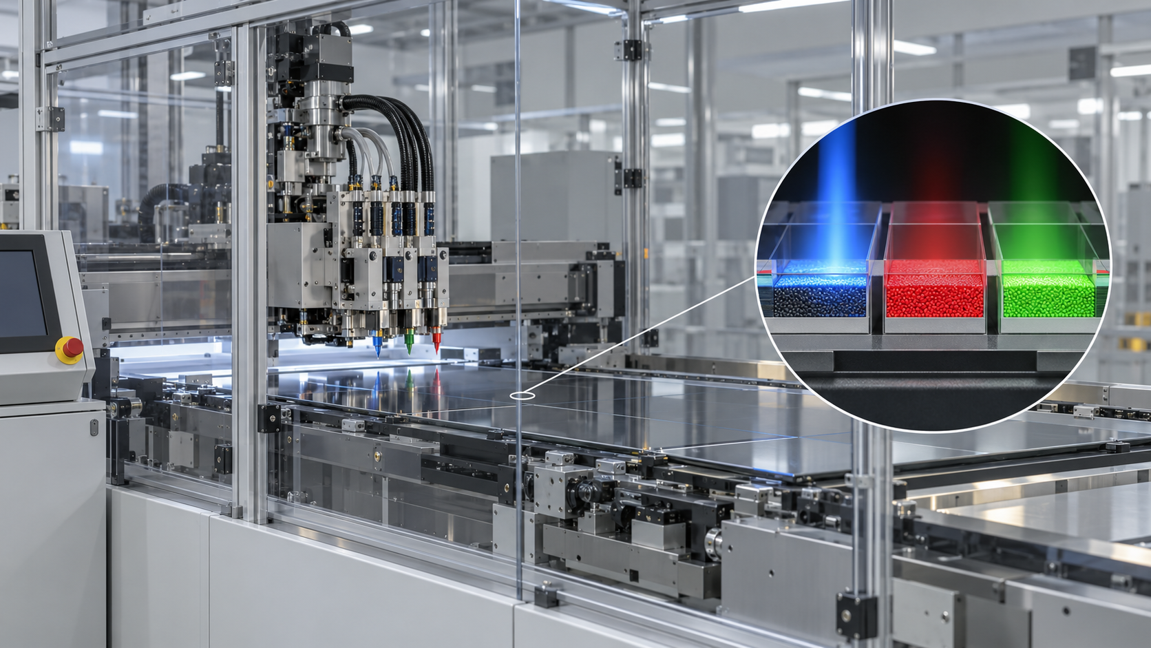
Samsung Electronics is a diversified electronics maker spanning smartphones, TVs, memory, foundry (contract chip manufacturing) and displays, and it touches nanotechnology in two main places. One is the QD-OLED panels made by its subsidiary Samsung Display (SDC, 84.8% owned by Samsung), where the company describes quantum dots as "semiconductor particles a few nanometers in size". The other is the GAA (gate-all-around) transistors mass-produced by its foundry business, which the company says reached mass production at 3 nm in 2022 and at 2 nm in 2025. Consolidated 2025 revenue was KRW 333.6 trillion, and R&D spending was KRW 37.75 trillion (11.3% of revenue). However, stand-alone foundry revenue, GAA yields and QD-OLED revenue do not appear in the official material this article reviewed. Separate from our profiles of the company in other fields, this one takes the view of quantum-dot displays and nanosheet transistors and sets out, from the company's own official material, what it makes, where it invests, who it works with, and which parts are results and which are plans. It is not investment advice.
- Samsung Electronics in 30 seconds, and where it stands in nanotechnology
- The logo and how the name is written
- Where the company sits in the field
- Scale (centered on what relates to nanotechnology)
- Resources committed to nanotechnology
- What it has done so far
- What comes next
- What the company is aiming for in nanotechnology
- Map of partnerships in nanotechnology
- Technologies, products and services
- The risks this company carries
- Glossary, references and claim-to-source audit
1. Samsung Electronics in 30 seconds, and where it stands in nanotechnology
GDRs on the London Stock ExchangePer the company's investor relations site
Most of Samsung Electronics' revenue comes from memory, smartphones and TVs, and revenue from the businesses most closely tied to nanotechnology (foundry GAA and QD-OLED) is not disclosed separately Not yet confirmed. Of consolidated revenue of KRW 171.5 trillion in April to June 2026, the DS (semiconductor) division accounted for KRW 127.5 trillion and memory alone for KRW 120.8 trillion (foundry and System LSI revenue appears to sit within the remaining KRW 6.7 trillion or so, but the company does not give that breakdown) Sourced. In other words, the company is not a nano specialist; nano-related businesses are a small part of a much larger whole. Even so, it says it was the first in the world to mass-produce 3 nm GAA, in 2022, and it names 2 nm GAA and QD-OLED as pillars of its technological competitiveness Sourced. Expressions such as "world's first" are the company's self-assessment, with no third-party confirmation attached.
2. The logo and how the name is written

A note on names: the formal name is Samsung Electronics Co., Ltd., abbreviated SEC. Samsung Display (SDC) is a subsidiary (84.8% owned) and a separate legal entity. MBCFET, SAFE, ISOCELL, Exynos, QD-OLED and Neo QLED are product, technology and brand names. The logo was taken from the company's official Foundry site (the original is white, a version for dark backgrounds).
Official site: https://semiconductor.samsung.com/foundry/3. Where the company sits in the field
The main type is devices & displays (turning nanostructures into products). The nanoscale-related businesses, as arranged from the company's material, are below Sourced.
| Area | What is nanoscale about it | What the company's material confirms | Type |
|---|---|---|---|
| Foundry GAA (3-nanometer and 2-nanometer generations) | Transistors whose channels are thin plate-like sheets (nanosheets), stacked and surrounded by the gate (GAA) | Mass production of 3 nm GAA in 2022 (the company says "a world's first"). Second-generation 3 nm GAA in March 2025 and first-generation 2 nm GAA in September 2025. The official site says SF2 (the 2 nm generation) started mass production in 2025 | Sourced (company statement) |
| QD-OLED (SDC) | An organic EL panel that uses quantum dots (semiconductor particles a few nanometers in size) to tune color | The company says it maximizes color gamut and viewing angle. Made with precision inkjet printing. A 27-inch QHD 500 Hz panel was developed in May 2025, among others | Sourced (company statement) |
| Nano-optics in image sensors (secondary) | Fine pixels (0.5 to 1.0 µm) and nano prism technology | The ISOCELL JNP (nano prism) improves sensitivity by 25% over the previous JN5 (announcements through October 2025, company statement) | Sourced (company statement) |
Percentages and other figures in the table are manufacturer's stated values; the baseline for each comparison (for example the 5 nm-generation process) and the measurement conditions are not described in detail. Reference: Reference 1 https://images.samsung.com/is/content/samsung/assets/global/ir/docs/2026_Half_Interim_Report.pdf Reference 3 https://news.samsung.com/global/samsung-begins-chip-production-using-3nm-process-technology-with-gaa-architecture Reference 4 https://semiconductor.samsung.com/foundry/process-technology/logic-node/ Reference 2 https://images.samsung.com/is/content/samsung/assets/global/ir/docs/2026_2Q_conference_eng.pdf
In short, the nanoscale core is the transistor structure (GAA) and the quantum-dot emissive layer (QD-OLED). The company's TV range also includes a product family named QLED, but how quantum dots are used there (for example, color conversion in an LCD backlight) is not described in the material this article reviewed Not yet confirmed.
4. Scale (centered on what relates to nanotechnology)
Samsung Electronics is a very large electronics company. The company as a whole is summarized briefly, with the focus on figures tied to nano-related businesses (the DS division, which includes the foundry, and SDC) Sourced.
| Indicator | Value | Note |
|---|---|---|
| Consolidated revenue (2025) | KRW 333.6 trillion | 2024 was KRW 300.9 trillion. Revenue by business includes inter-division transactions; the company total is after eliminations |
| Consolidated revenue (first half of 2026) | KRW 305.4 trillion | +98.7% year on year. DS division +294.7%, SDC +15.8% (company statement) |
| Operating profit (April to June 2026) | KRW 89.5 trillion | Operating margin 52.2%. January to March was KRW 57.2 trillion, so the first half totals KRW 146.7 trillion (our calculation) |
| DS division (semiconductors) revenue (April to June 2026) | KRW 127.5 trillion | Memory KRW 120.8 trillion. Foundry alone is not disclosed. Operating profit KRW 89.2 trillion |
| SDC (displays) revenue (April to June 2026) | KRW 7.5 trillion | Operating profit KRW 0.7 trillion. 2025 revenue was KRW 29.84 trillion |
| R&D expenses | KRW 37.75 trillion in 2025 | 11.3% of revenue. April to June 2026: KRW 16.0 trillion (9.3%). The nano-related share is not disclosed |
| Capital expenditure (first half of 2026) | About KRW 28.0 trillion | DS division KRW 25.60 trillion, SDC KRW 1.33 trillion, others KRW 1.05 trillion |
| Patents held | 296,468 (worldwide) | As of 30 June 2026. Covers all businesses; the nano-related count is not disclosed |
| Employees (Korean headquarters, stand-alone) | 129,200 | 30 June 2026. A consolidated total was not found in the material reviewed |
Reference: Reference 1 https://images.samsung.com/is/content/samsung/assets/global/ir/docs/2026_Half_Interim_Report.pdf Reference 2 https://images.samsung.com/is/content/samsung/assets/global/ir/docs/2026_2Q_conference_eng.pdf
The surge in revenue and profit in 2026 is attributed by the company mainly to memory demand for AI, not to GAA or QD-OLED Sourced. A memory boom can make nano-related businesses look stronger than they are. The half-year report also uses figures from a research firm (Omdia) for display market volumes, but this article does not adopt research-firm estimates. "3-nanometer" and "2-nanometer" are the company's generation names and do not imply performance comparable with similarly named generations at other companies.
5. Resources committed to nanotechnology
Headcount, R&D and capex devoted to nano-related businesses alone are not disclosed. The table below shows company-wide disclosures.
| Resource | What primary sources confirm | Type |
|---|---|---|
| People | 129,200 employees at the Korean headquarters (stand-alone, 30 June 2026). R&D is organized in three layers: business-unit R&D (1 to 2 years ahead), research institutes (Samsung Research and semiconductor research centers, 3 to 5 years ahead) and the company-wide institute SAIT (Samsung Advanced Institute of Technology). Overseas R&D sites include the U.S., Ukraine, Japan, China, India and Israel. Nano-related headcount is not disclosed | Sourced / partly undisclosed |
| Money (R&D) | 2025 R&D spending was KRW 37.75 trillion (11.3% of revenue), and KRW 27.36 trillion in the first half of 2026. Government subsidies were about KRW 14.4 billion in 2025 (0.04% of R&D: our calculation) and are deducted from R&D expenses. The nano-related breakdown is not disclosed | Sourced / partly undisclosed |
| Money (capex) | Capital expenditure in the first half of 2026 was about KRW 28.0 trillion, which the company says concentrated on "capacity expansions and tech migration for advanced nodes/processes, as well as infrastructure" in the DS division and SDC. By division: DS KRW 25.60 trillion and SDC KRW 1.33 trillion. Capex for foundry or QD-OLED alone is not disclosed | Sourced / partly undisclosed |
| Equity stakes, acquisitions, joint ventures, divestments | It holds 84.8% of SDC (subsidiary). On 31 January 2024 SDC sold the 56.8% stake in DOWOOINSYS held by two Samsung Venture Investment funds (which the company says was to focus on its main business and R&D amid intensified OLED competition). A Texas semiconductor-manufacturing subsidiary, SAS. No major nano-related acquisition was found in the material reviewed | Sourced / not found |
| Universities, research institutes and public funding | Through SAFE (the Samsung Advanced Foundry Ecosystem) with EDA companies (Ansys, Cadence, Siemens, Synopsys), Samsung has offered a design environment for 3 nm GAA since the third quarter of 2021 (2022 announcement). The half-year report gave no specific university or research consortium that we could confirm. Public funding is small: government subsidies against R&D | Sourced / partly not found |
Reference: Reference 1 https://images.samsung.com/is/content/samsung/assets/global/ir/docs/2026_Half_Interim_Report.pdf Reference 3 https://news.samsung.com/global/samsung-begins-chip-production-using-3nm-process-technology-with-gaa-architecture
Status of main products and facilities
| Product / facility | Site / content | Scale | Stage | Date | Reference |
|---|---|---|---|---|---|
| 3 nm GAA (MBCFET) | Foundry. Nanosheet transistors | Comparison figures in the note below | Initial production started (first generation). The second generation is in mass production | 30 June 2022 / March 2025 | 3, 1 |
| 2 nm GAA (SF2) | Foundry. Starting with mobile | Performance +5%, power -8%, area -5% (versus second-generation 3 nm; company statement) | Mass production (first generation). Second-generation mobile products are planned for mass production in the second half of 2026 | September 2025 / second half of 2026 | 1, 4, 2 |
| Exynos 2600 | A mobile chip on the 2 nm GAA process | CPU performance +39% over the previous model, Exynos 2500 (company statement) | Announced (the company calls it "the industry's first") | Announcements through March 2026 | 1 |
| Foundry manufacturing sites | South Korea: Giheung, Hwaseong, Pyeongtaek. U.S.: Austin and Taylor in Texas | Capacity per site is not disclosed | The operating status of Taylor could not be confirmed | Checked 9 October 2026 | 5 |
| Large QD-OLED panels | SDC. 27-inch QHD 500 Hz and others | Output across all SDC panels was 899 thousand units (8th-generation glass equivalent) in the first half of 2026 | Mass production. Mass production of the 8.6th-generation IT OLED line is planned | 2025 to 2026 | 1, 2 |
Note on comparison figures (company statements): second-generation 3 nm GAA reduced area by 35% and power by over 40% and improved performance by up to 30% versus the 5 nm-generation process (half-year report, March 2025). The 2022 announcement gave the second-generation 3 nm as "power -50%, performance +30%, area -35%" as targets, which differs from the post-production statement (power over 40% lower). Measurement conditions are not stated.
6. What it has done so far
| When | What happened | Why it matters |
|---|---|---|
| 13 January 1969 | Established as Samsung Electronics Industry Co., Ltd.; listed through an IPO in 1975 | The starting point of the electronics group |
| 30 June 2022 | Started initial production of the 3 nm GAA process (MBCFET). It described applying the nanosheet transistor first to high-performance, low-power computing and then expanding to mobile | The move to the structure that follows FinFET |
| 2022 | Held a groundbreaking ceremony for a next-generation semiconductor R&D complex. Mass-produced 3 nm GAA (recorded by the company as "a world's first") | Investment in advanced research |
| 31 January 2024 | SDC sold the 56.8% stake in DOWOOINSYS held by two Samsung Venture Investment funds | Focusing on the OLED business |
| March 2025 | Mass-produced the second-generation 3 nm GAA | An improved generation of GAA |
| May 2025 | Developed a 27-inch QHD 500 Hz QD-OLED display (described as the highest self-emissive refresh rate) | Speeding up QD-OLED |
| 26 July 2025 | Disclosed a semiconductor contract manufacturing supply agreement with Tesla, Inc. (July 2025 to December 2033, US$16,544 million) | A large foundry contract |
| September 2025 | Mass-produced the first-generation 2 nm GAA (optimized for mobile) | The 2-nanometer nanosheet generation |
| 2025 | The official site records that SF2 started mass production | A foundry generation name |
| April to June 2026 | The foundry reports higher utilization and stronger advanced-node demand, and is working to expand orders from major data center customers for 2 nm | The 2 nm generation for HPC |
Reference: Reference 1 https://images.samsung.com/is/content/samsung/assets/global/ir/docs/2026_Half_Interim_Report.pdf Reference 3 https://news.samsung.com/global/samsung-begins-chip-production-using-3nm-process-technology-with-gaa-architecture Reference 4 https://semiconductor.samsung.com/foundry/process-technology/logic-node/ Reference 2 https://images.samsung.com/is/content/samsung/assets/global/ir/docs/2026_2Q_conference_eng.pdf
7. What comes next
All of the above are company plans, outlooks and targets Not yet confirmed. For the foundry the company says it is "establishing tailored strategies for each node and application" and expects advanced nodes to drive revenue growth. In April to June 2026 memory made up most of revenue, and this article reads the nano-related plans as not being what determines the company's overall results Inference.
None of the following appears in the official material this article reviewed Not yet confirmed.
Foundry revenue and profit / GAA yield and monthly output / the names of 2 nm customers other than Tesla / QD-OLED revenue and unit sales / the sourcing and composition of quantum dot materials (such as whether cadmium is used) / nano-related R&D spending and headcount / the operating status of the Taylor fab / the sales impact in won of export controls and tariffs.
8. What the company is aiming for in nanotechnology
This section separates what the company says directly from what this article reads into it. Inference marks this article's own interpretation of primary sources.
| What can be read | Primary source behind it | Type |
|---|---|---|
| It is widening GAA from 3 nm to 2 nm, and from mobile to AI/HPC | In 2022 it described applying 3 nm GAA first to high-performance, low-power computing and expanding to mobile. In 2026 it mentions 2 nm mobile mass production alongside 2 nm HPC engagements and expanding orders from major data center customers | Sourced |
| It optimizes design and manufacturing together (DTCO) | The 2022 announcement and the 2025 description of 2 nm GAA both cite design-technology co-optimization (DTCO). The design environment is built with SAFE partners | Sourced |
| In large panels it is concentrating on premium QD-OLED products | Half-year report: the large panel business focuses on high-performance QD-OLED premium products and is expanding its gaming monitor customer base | Sourced |
| Vertical integration: its own chips and its own products together | It announced the Exynos 2600 (its own mobile AP) on 2 nm GAA, while the foundry also has external customers such as Tesla | Sourced / Inference (the framing as vertical integration) |
| It uses nano-optics (nano prism) as a way to shrink image sensor pixels | It announced the ISOCELL JNP (nano prism) as "the industry's first" and also a 0.5 µm, 200-megapixel sensor | Sourced (company statement) |
The reading that "Samsung Electronics runs a two-sided strategy, using nano-related technology both to differentiate its own products (smartphones, monitors) and to sell to outside customers" rests on the same technology appearing in two forms. GAA is used in its own Exynos 2600 and also sold under foundry contracts with outside customers such as Tesla (through December 2033) Sourced. QD-OLED appears to be supplied through SDC not only for its own TVs and monitors but to outside brands as well, though no outside customer is named in the material reviewed. This article therefore reads its nano-related investment as aiming at differentiation of its own products and utilization secured through contract manufacturing at the same time Inference Not yet confirmed.
9. Map of partnerships in nanotechnology
10. Technologies, products and services
The nano-related "products" are foundry process technology, SDC's QD-OLED panels, image sensors and chips of its own design Sourced. The table below lists what the company's material says; performance figures are manufacturer's stated values.
| Technology / product | What the material says | Reference |
|---|---|---|
| 3 nm GAA (MBCFET) | The "Multi-Bridge-Channel FET" is Samsung's GAA. It uses nanosheets with wider channels, which the company says gives higher performance and energy efficiency than GAA built on narrower nanowires, and the nanosheet channel width can be adjusted to optimize power and performance for each customer. First-generation 3 nm: power up to 45% lower, performance 23% higher and area 16% smaller versus 5 nm (2022 announcement, company claim) | 3 |
| 2 nm GAA (SF2) | First generation: performance +5%, power -8%, area -5% versus second-generation 3 nm (company statement). Starting with mobile. The company says DTCO delivers high performance and low power. The official site records SF2 mass production (2025) | 1, 4 |
| QD-OLED panels (SDC) | A self-emissive display using quantum dots. 27-inch (QHD 500 Hz, UHD 160 ppi and others) and 31.5-inch (UHD 140 ppi) panels were developed. Made with precision inkjet printing | 1 |
| TVs and monitors (QD-OLED, Neo QLED) | A QD-OLED TV (S95, 4K), QD-OLED gaming monitors (4K 240 Hz, 500 Hz) and Neo QLED (LCD using Mini LED). The new LED in Neo QLED is described as a "Quantum Nano-Layer Multi-Cell" structure (how quantum dots are used is not stated) | 1 |
| Image sensors (ISOCELL) | The ISOCELL JNP uses nano prism technology and is 25% more sensitive than the earlier JN5. The HP5 is 0.5 µm and 200 megapixels. Pixels are separated by deep trenches such as FDTI | 1 |
| Design environment (SAFE) | A design environment for 3 nm GAA built with Ansys, Cadence, Siemens EDA, Synopsys and others | 3 |
The company's material points to three places where materials matter. (1) The nanosheet channel: Samsung says it uses wider nanosheets than nanowire-based GAA, and optimizes power and performance by adjusting channel width Sourced. This article expects sheet thickness and stacking uniformity to affect device variation, but the official material gives no figures on yield or defects Inference Not yet confirmed. (2) The quantum-dot emissive layer: QD-OLED uses semiconductor particles a few nanometers in size to tune color. Variation in particle size, surface treatment and dispersion could affect color purity and lifetime, but the composition of the quantum dot materials (whether they contain cadmium) and their suppliers are not stated Not yet confirmed. (3) Inkjet-formed films: the company says it makes high-definition (140 to 160 ppi) QD-OLED with precision inkjet printing Sourced. The viscosity of the ink, how it dries and the uniformity of film thickness bear directly on how well each pixel turns out Inference. For the basics, see our explainers on quantum dots, nanoscale transistors, and nanocoatings and thin films.
Reference: Reference 3 https://news.samsung.com/global/samsung-begins-chip-production-using-3nm-process-technology-with-gaa-architecture Reference 1 https://images.samsung.com/is/content/samsung/assets/global/ir/docs/2026_Half_Interim_Report.pdf Reference 4 https://semiconductor.samsung.com/foundry/process-technology/logic-node/
11. The risks this company carries
| Risk | What it involves | Type |
|---|---|---|
| Nano-related results are not visible | Foundry and QD-OLED revenue, GAA yield and customer counts are not published. Expressions such as "world's first" are self-assessments with no third-party confirmation | Sourced (not found) |
| An earnings structure that depends on memory | In April to June 2026 memory accounted for about 70% of consolidated revenue (memory revenue divided by consolidated revenue, an approximation because it includes inter-division transactions: our calculation), and the DS division for most of operating profit. If the memory market turns, the company's results change, and so may its capacity to invest in nano-related businesses | Sourced / Inference |
| Competition in foundry | The company says only about five companies with large capex dominate the foundry market. Winning 2 nm customers and keeping utilization up are critical | Sourced |
| Dependence on specific large contracts | The Tesla contract is US$16,544 million (July 2025 to December 2033). The company says the period and amount may change with demand and performance | Sourced / Inference |
| Rising component costs | The DX division posted an operating loss (KRW -0.8 trillion) in April to June 2026 because of rising component costs. This could also weigh on the profitability of TVs and monitors that use QD-OLED | Sourced / Inference |
| Geopolitics and regulation | The company says demand for domestic sourcing in China is likely to persist. The effect of tariffs and export controls on sales in won could not be confirmed. "Tariffs" appears among the Q&A topics of an investor relations meeting | Sourced / not found |
| Delivery of plans | Mass production of second-generation 2 nm, the 8.6th-generation OLED line and double-digit foundry growth are all company plans and targets, and their achievement has not been confirmed | Not yet confirmed |
Reference: Reference 1 https://images.samsung.com/is/content/samsung/assets/global/ir/docs/2026_Half_Interim_Report.pdf Reference 2 https://images.samsung.com/is/content/samsung/assets/global/ir/docs/2026_2Q_conference_eng.pdf
12. Glossary
- GAA (gate-all-around)
- A transistor structure in which the gate surrounds the channel on all sides. The structure that follows FinFET.
- Nanosheet / MBCFET
- A kind of GAA in which the channel is made of thin stacked sheets. MBCFET is a Samsung trademark.
- DTCO
- Optimizing design and manufacturing technology together.
- Quantum dot
- A semiconductor particle a few nanometers in size. Its size tunes the color (wavelength) of light.
- QD-OLED
- An organic EL display that uses quantum dots to tune color (company description).
- SDC
- Samsung Display Co., Ltd., a subsidiary 84.8% owned by Samsung Electronics.
- ISOCELL
- Samsung's image sensor brand.
- SAFE
- Samsung Advanced Foundry Ecosystem, a framework of design tool and IP partners.
- SF2
- The process name for Samsung Foundry's 2 nm generation.
- HPC
- High-performance computing, such as chips for AI.
13. References
- Samsung Electronics Samsung Electronics Business Report (half-year report, as of 30 June 2026). Company overview, revenue by business, R&D spending, capex, intellectual property, market conditions, major contracts, and R&D results (foundry GAA, display QD-OLED). https://images.samsung.com/is/content/samsung/assets/global/ir/docs/2026_Half_Interim_Report.pdf
- Samsung Electronics 2Q 2026 Earnings Call (results presentation for April to June 2026). Results and outlook by business, and the foundry and display sections. https://images.samsung.com/is/content/samsung/assets/global/ir/docs/2026_2Q_conference_eng.pdf
- Samsung Electronics News release "Samsung Begins Chip Production Using 3nm Process Technology With GAA Architecture" (30 June 2022). https://news.samsung.com/global/samsung-begins-chip-production-using-3nm-process-technology-with-gaa-architecture
- Samsung Electronics Official site, "Foundry - Logic Node" (checked 9 October 2026). The statement that SF2 started mass production. https://semiconductor.samsung.com/foundry/process-technology/logic-node/
- Samsung Electronics Official site, "Foundry - Manufacturing Sites" (checked 9 October 2026). List of foundry manufacturing sites. https://semiconductor.samsung.com/foundry/manufacturing/manufacturing-sites/
- Samsung Electronics Official investor site, "Listing Information". Listing venues. https://www.samsung.com/global/ir/stock-information/listing-Info/
- Samsung Electronics Official site, "Foundry" (source of the logo image). https://semiconductor.samsung.com/foundry/
14. Claim-to-source audit
| Claim in the text | Type | Reference |
|---|---|---|
| Legal name, establishment (13 January 1969), IPO (11 June 1975), headquarters (Suwon) and listing (Korea Exchange; GDRs in London) | Sourced | Reference 1 https://images.samsung.com/is/content/samsung/assets/global/ir/docs/2026_Half_Interim_Report.pdf Reference 6 https://www.samsung.com/global/ir/stock-information/listing-Info/ |
| Consolidated revenue of KRW 333.6 trillion in 2025, KRW 300.9 trillion in 2024 and KRW 305.4 trillion in the first half of 2026 (+98.7% year on year) | Sourced | Reference 1 https://images.samsung.com/is/content/samsung/assets/global/ir/docs/2026_Half_Interim_Report.pdf |
| April to June 2026: revenue of KRW 171.5 trillion, operating profit of KRW 89.5 trillion, DS KRW 127.5 trillion, memory KRW 120.8 trillion, SDC KRW 7.5 trillion | Sourced | Reference 2 https://images.samsung.com/is/content/samsung/assets/global/ir/docs/2026_2Q_conference_eng.pdf |
| First-half operating profit of KRW 146.7 trillion, the 0.04% government-subsidy share of R&D, and memory at about 70% of consolidated revenue | Our calculation | Our calculation from the figures in the references. Reference 2 https://images.samsung.com/is/content/samsung/assets/global/ir/docs/2026_2Q_conference_eng.pdf Reference 1 https://images.samsung.com/is/content/samsung/assets/global/ir/docs/2026_Half_Interim_Report.pdf |
| Foundry revenue and profit, and QD-OLED revenue and unit sales | Not yet confirmed | No statement found within the scope of this article's review. Not estimated here. |
| R&D spending (KRW 37.75 trillion in 2025, 11.3% of revenue; KRW 27.36 trillion in the first half of 2026) and government subsidies of KRW 14.4 billion | Sourced | Reference 1 https://images.samsung.com/is/content/samsung/assets/global/ir/docs/2026_Half_Interim_Report.pdf |
| Capex (about KRW 28.0 trillion in the first half of 2026; DS KRW 25.60 trillion; SDC KRW 1.33 trillion) | Sourced | Reference 1 https://images.samsung.com/is/content/samsung/assets/global/ir/docs/2026_Half_Interim_Report.pdf |
| 296,468 patents held, the R&D organization (SAIT, Samsung Research and others) and 129,200 employees at the Korean headquarters | Sourced | Reference 1 https://images.samsung.com/is/content/samsung/assets/global/ir/docs/2026_Half_Interim_Report.pdf |
| The 84.8% stake in SDC, SDC revenue (KRW 29.84 trillion in 2025) and the sale of the 56.8% DOWOOINSYS stake (31 January 2024) | Sourced | Reference 1 https://images.samsung.com/is/content/samsung/assets/global/ir/docs/2026_Half_Interim_Report.pdf |
| Initial production of 3 nm GAA (MBCFET) on 30 June 2022, the nanosheet features, and first- and second-generation comparison figures (targets) | Sourced | The comparison figures are 2022 targets. Measurement conditions are not stated. Reference 3 https://news.samsung.com/global/samsung-begins-chip-production-using-3nm-process-technology-with-gaa-architecture |
| Mass production of 3 nm GAA (2022) and of the second generation (March 2025: area -35%, power over 40% lower, performance up to +30%) | Sourced | Comparison figures are the company's statements. Reference 1 https://images.samsung.com/is/content/samsung/assets/global/ir/docs/2026_Half_Interim_Report.pdf |
| Mass production of first-generation 2 nm GAA (September 2025: performance +5%, power -8%, area -5%) and the Exynos 2600 (2 nm GAA) | Sourced | Comparison figures are the company's statements. Reference 1 https://images.samsung.com/is/content/samsung/assets/global/ir/docs/2026_Half_Interim_Report.pdf |
| The statement that SF2 started mass production in 2025 | Sourced | Reference 4 https://semiconductor.samsung.com/foundry/process-technology/logic-node/ |
| Planned second-generation 2 nm mobile mass production (second half of 2026), 4 nm ramp-up, the target of double-digit foundry growth and the planned 8.6th-generation OLED line | Not yet confirmed | Company plans and targets. Reference 2 https://images.samsung.com/is/content/samsung/assets/global/ir/docs/2026_2Q_conference_eng.pdf Reference 1 https://images.samsung.com/is/content/samsung/assets/global/ir/docs/2026_Half_Interim_Report.pdf |
| The Tesla semiconductor contract manufacturing supply agreement (July 2025 to December 2033, US$16,544 million) | Sourced | The company says the period and amount may change. Reference 1 https://images.samsung.com/is/content/samsung/assets/global/ir/docs/2026_Half_Interim_Report.pdf |
| Foundry manufacturing sites (Giheung, Hwaseong, Pyeongtaek, Austin, Taylor) | Sourced | Operating status of Taylor not stated. Reference 5 https://semiconductor.samsung.com/foundry/manufacturing/manufacturing-sites/ |
| QD-OLED description (semiconductor particles a few nanometers in size; color gamut and viewing angle), the 27-inch QHD 500 Hz panel and others, and precision inkjet printing | Sourced | Reference 1 https://images.samsung.com/is/content/samsung/assets/global/ir/docs/2026_Half_Interim_Report.pdf |
| ISOCELL JNP (nano prism, sensitivity +25%) and HP5 (0.5 µm, 200 megapixels) | Sourced | Comparison figures are the company's statements. Reference 1 https://images.samsung.com/is/content/samsung/assets/global/ir/docs/2026_Half_Interim_Report.pdf |
| SAFE partners (Ansys, Cadence, Siemens, Synopsys) and the 3 nm GAA design environment offered since the third quarter of 2021 | Sourced | Reference 3 https://news.samsung.com/global/samsung-begins-chip-production-using-3nm-process-technology-with-gaa-architecture |
| Patent cross-licenses (Google, Nokia, Qualcomm and others) and five major customers accounting for about 25% of company-wide sales | Sourced | Reference 1 https://images.samsung.com/is/content/samsung/assets/global/ir/docs/2026_Half_Interim_Report.pdf |
| The DX division's operating loss in April to June 2026 (rising component costs), foundry competition (about five companies) and demand for domestic sourcing in China | Sourced | Reference 2 https://images.samsung.com/is/content/samsung/assets/global/ir/docs/2026_2Q_conference_eng.pdf Reference 1 https://images.samsung.com/is/content/samsung/assets/global/ir/docs/2026_Half_Interim_Report.pdf |
| GAA yield and monthly output, customers other than Tesla, the composition and sourcing of quantum dot materials, and the effect of tariffs and export controls on sales | Not yet confirmed | No statement found within the scope of this article's review. |
| The readings that nano-related technology serves both its own products and outside customers, and that its earnings depend on memory | Inference | This article's interpretation of the statements in the references. Reference 1 https://images.samsung.com/is/content/samsung/assets/global/ir/docs/2026_Half_Interim_Report.pdf Reference 2 https://images.samsung.com/is/content/samsung/assets/global/ir/docs/2026_2Q_conference_eng.pdf Reference 3 https://news.samsung.com/global/samsung-begins-chip-production-using-3nm-process-technology-with-gaa-architecture |
| The reading that nanosheet thickness and stacking, quantum-dot particle variation and inkjet ink behavior bear on performance | Inference | This article's own commentary. The references do not state it directly. Reference 3 https://news.samsung.com/global/samsung-begins-chip-production-using-3nm-process-technology-with-gaa-architecture Reference 1 https://images.samsung.com/is/content/samsung/assets/global/ir/docs/2026_Half_Interim_Report.pdf |
| Samsung Electronics' type (devices and displays) and the categories in Fig. 1 | Our calculation | This article's own arrangement. Company names are examples drawn from this series. |
Last updated 9 October 2026 / Troy Technical
Figures in this article come from Samsung Electronics' half-year report for 2026, its 2Q 2026 earnings presentation, the official site and a 2022 news release. No research-firm estimates (including those cited in the half-year report) or press-based figures have been used. Passages marked "Inference" are this article's interpretation of primary sources, not statements made by the company. Company plans, targets and outlooks (mass production timing, growth targets, new lines) are unconfirmed forward-looking statements. Expressions such as "world's first" and "industry's first" are the company's self-assessments. "3 nm" and "2 nm" are the company's generation names and do not imply comparison with other companies. This article is not investment advice.