COMPANY PROFILE / NANOTECHNOLOGY
Tokyo Electron
A semiconductor equipment maker whose tools coat, etch, deposit and clean nanometer-scale circuit patterns in leading-edge logic and memory fabs
Tokyo Electron (TEL) belongs in a nanotechnology series because it makes the tools that form chip circuits at feature sizes of a few to a few tens of nanometers. In the fiscal year ended March 2026 (fiscal 2026) it reported net sales of ¥2,443.5 billion and had 20,236 employees. Of its new-equipment sales (¥1,775.4 billion), 36% was etch, 28% coater/developer, 20% deposition and 9% cleaning. Its largest customers were Samsung Electronics (15.1% of sales) and TSMC (12.9%), and China accounted for 34.1% of sales by region. TEL does not report what share of sales is "nano", and almost all of its equipment sales relate to nanoscale processing. This profile sets out, from the company's own official material, what it makes, where it invests, who it works with, and which parts are results and which are plans. It is not investment advice.
- Tokyo Electron in 30 seconds, and where it stands in nanotechnology
- The logo and how the name is written
- Where the company sits in the field
- Scale (centered on what relates to nanoscale processing)
- Resources committed to nanotechnology
- What it has done so far
- What comes next
- What the company is aiming for in nanotechnology
- Map of partnerships in nanotechnology
- Technologies, products and services
- The risks this company carries
- Glossary, references and claim-to-source audit
1. Tokyo Electron in 30 seconds, and where it stands in nanotechnology
Prime Market (8035)Listed on the Prime Market in 2022, per the company history
TSMC 12.9%Share of fiscal 2026 net sales, including subsidiaries
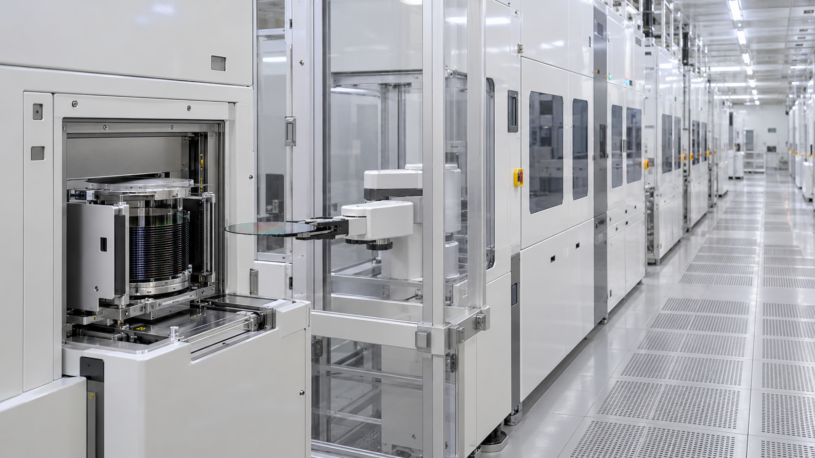
TEL is not a company that makes nanoscale circuits itself. It supplies the equipment that its customers, the chipmakers, use in their own fabs to make them. In the process diagram of its Integrated Report, TEL products appear for deposition, resist coating and development, etch, cleaning, wafer bonding and inspection (probers). The exposure step, where light prints the circuit pattern, carries no TEL product Sourced. What sets TEL apart is that it covers the steps on either side of exposure: coat (resist), etch, deposit and clean. The company says it holds a 100% share of coater/developers used with EUV (extreme ultraviolet) exposure (the company's own estimate) Sourced. That 100% is TEL's self-estimate, not a third-party statistic, so this article reports it as a company claim and not as established fact.
2. The logo and how the name is written

A note on names: the company's formal name is Tokyo Electron Limited (abbreviated TEL). Many subsidiaries and sites carry the TEL name (Tokyo Electron Miyagi, Tokyo Electron Kyushu, TEL Technology Center America and others). The similarly named Tokyo Electron Device is a separate listed company and is not covered here. The logo was taken from the company's official website (tel.com).
Official site: https://www.tel.com/3. Where the company sits in the field
TEL's type is nanofabrication & equipment. Its official site describes its development sites as places that address "complex and diversifying nanoscale technology needs" Sourced, but TEL does not split its business by "nanotechnology" (see Reference 8 https://www.tel.com/rd/base/index.html). The table below is this article's own arrangement of TEL's disclosures, cut by processes that machine nanoscale circuits.
| Process (product group) | Role in nanoscale processing | Share of new-equipment sales (FY2026) | Type |
|---|---|---|---|
| Etch | Removes film along the pattern drawn in resist to form trenches and holes. In DRAM and NAND this includes deep, narrow holes (high aspect ratio) | 36% (about ¥639 billion) | Sourced |
| Coater/developer | Coats resist evenly on the wafer and develops it after exposure to reveal the pattern. Used together with EUV exposure | 28% | Sourced |
| Deposition | Builds up oxide, nitride and metal films by CVD or ALD (atomic layer deposition) | 20% | Sourced |
| Cleaning | Removes resist residue and particles left after etching | 9% | Sourced |
| Wafer probers and others | Tests finished wafers (probers) and other equipment | Probers 5%, others 2% | Sourced |
Shares are of new-equipment (semiconductor production equipment) sales of ¥1,775.4 billion and exclude field solutions (used equipment, modifications, parts and services; ¥626.0 billion). Yen amounts are approximations from the rounded integer percentages Our calculation. Reference: Reference 5 https://www.tel.com/ir/library/ar/g4alje00000000pq-att/ir2026_data_section_en.pdf
In short, the center of gravity is the patterning steps for leading-edge logic (chips for AI) and for DRAM and NAND memory. By application, non-memory (logic, foundry and others) was 59%, DRAM 31% and NAND 10% of fiscal 2026 new-equipment sales Sourced.
4. Scale (centered on what relates to nanoscale processing)
TEL is a large equipment maker. The company as a whole is summarized briefly, and the focus is the disclosed breakdown by product and by application Sourced. As far as this article could confirm in the Integrated Report, TEL does not report separate business segments, and sales attributable to nanotechnology alone are not disclosed.
| Indicator (fiscal 2026, year ended March 2026) | Value | Note |
|---|---|---|
| Net sales | ¥2,443,533 million | +0.5% year on year, a record for the second year in a row. Fiscal 2025 was ¥2,431.5 billion |
| Operating income | ¥624,936 million | -10.4% year on year. Operating margin 25.6% (28.7% the year before) |
| Net income attributable to owners of parent | ¥574,454 million | A record. Includes a ¥115,494 million gain on sale of investment securities |
| New-equipment (semiconductor production equipment) sales | ¥1,775.4 billion | Etch 36%, coater/developer 28%, deposition 20%, cleaning 9%, probers 5%, others 2% |
| Field solutions (modifications, used equipment, parts, service) | ¥626.0 billion | Used equipment and modifications ¥190.0 billion; parts and services ¥435.9 billion |
| R&D expenses | ¥277.9 billion | +11.1% year on year (up ¥27,849 million). About 11.4% of net sales (our calculation) |
| Capital expenditure (company chart) | ¥216.0 billion | Fiscal 2027 plan: ¥190.0 billion (company outlook) |
| Employees (consolidated) | 20,236 | End of March 2026. The "Company Info" page of the official site gives 20,812 (consolidated); we could not confirm why the two differ (for example, the reference date) |
| Sales by region | China 34.1%, South Korea 22.3%, Taiwan 20.4% | Japan 9.8%, North America 6.8%, Southeast Asia and others 3.8%, Europe 2.8%. China was 41.7% the year before |
| Major customers | Samsung Electronics ¥368,079 million (15.1%) TSMC ¥315,813 million (12.9%) | Together 28.0% (our calculation). Includes sales to subsidiaries |
| Patents held | 26,592 | End of March 2026. Counted using the LexisNexis PatentSight+ database (company statement) |
Reference: Reference 5 https://www.tel.com/ir/library/ar/g4alje00000000pq-att/ir2026_data_section_en.pdf Reference 2 https://www.tel.com/ir/library/ar/g4alje00000000pq-att/ir2026_chapter2_en.pdf Reference 7 https://www.tel.com/about/summary/
TEL does not disclose a share of sales that is "nanotechnology" Not yet confirmed. The product-level yen amounts in this article (for example "about ¥639 billion") are approximations obtained by multiplying published rounded percentages, not figures published by the company Our calculation. New-equipment sales (¥1,775.4 billion) plus field solutions (¥626.0 billion) do not add up to consolidated net sales (¥2,443.5 billion). The gap of about ¥42.1 billion (our calculation) is not explained in the material this article reviewed.
5. Resources committed to nanotechnology
The headcount and R&D spending devoted to nanoscale processing alone are not disclosed. The table below lines up company-wide disclosures as the resources that feed nanoscale equipment development.
| Resource | What primary sources confirm | Type |
|---|---|---|
| People | 20,236 employees (consolidated, end of March 2026); engineers are 68.9%. There are 19 R&D sites (8 in Japan, 11 overseas). TEL plans to recruit 10,000 people worldwide over five years from fiscal 2025. Headcount for nanoscale processing alone is not disclosed | Sourced / partly undisclosed |
| Money (R&D) | Fiscal 2026 R&D expenses were ¥277.9 billion (¥250.0 billion the year before). The fiscal 2027 outlook is ¥330.0 billion. A five-year plan from fiscal 2025 calls for more than ¥1.5 trillion. Breakdown by product is not disclosed | Sourced / plan not yet confirmed |
| Money (capex) | Fiscal 2026 capital expenditure was ¥216.0 billion. In the same year, development buildings in Koshi (Kumamoto) and Taiwa (Miyagi) and a production and logistics center in Oshu (Iwate) were completed. The Miyagi Innovative Production Center (Kurokawa-gun, Miyagi) is scheduled for completion in summer 2027. The fiscal 2027 outlook is ¥190.0 billion, and the five-year plan is more than ¥700 billion | Sourced / plan not yet confirmed |
| Equity stakes, acquisitions, joint ventures, divestments | TEL Venture Capital invests in startups (the official site announced Phosio in May 2026 and Advance Composite in August 2026; other announcements do not name the company). On 30 June 2026 TEL announced a merger of two U.S. subsidiaries, Tokyo Electron America and TEL Technology Center, America (effective 1 July; an intra-group reorganization). In fiscal 2026 it sold part of its strategic shareholdings, booking a ¥115.5 billion gain. No large acquisition or joint venture related to nanoscale processing was found in the material reviewed | Sourced / not found |
| Universities, research institutes and public funding | TEL has worked with imec (Belgium) since 1995 and in June 2025 renewed the partnership for a new five-year phase. Other development sites and consortiums include NY CREATES Albany NanoTech Complex and BRIDG (U.S.), CEA-Leti (France), IME (Singapore) and AIST (Japan). TEL takes part in the U.S.-Japan university partnership UPWARDS. In September 2025 it announced a new development site in Bengaluru, India, and plans joint research with Indian universities. Amounts of public subsidies received were not found in the material reviewed | Sourced / partly not found |
Reference: Reference 1 https://www.tel.com/ir/library/ar/g4alje00000000pq-att/ir2026_chapter1_en.pdf Reference 2 https://www.tel.com/ir/library/ar/g4alje00000000pq-att/ir2026_chapter2_en.pdf Reference 3 https://www.tel.com/ir/library/ar/g4alje00000000pq-att/ir2026_chapter3_en.pdf Reference 5 https://www.tel.com/ir/library/ar/g4alje00000000pq-att/ir2026_data_section_en.pdf Reference 6 https://www.tel.com/ir/library/investors-guide/hq95qj0000000734-att/InvestorsGuide_E20260915_rev00.pdf Reference 8 https://www.tel.com/rd/base/index.html Reference 9 https://www.tel.com/rd/telvc/index.html Reference 22 https://www.tel.com/news/ir/2026/20260630_001.html Reference 10 https://www.tel.com/news/topics/2025/20250616_001.html Reference 21 https://www.tel.com/news/topics/2025/20250905_001.html
Status of main products and facilities
| Product / facility | Site / role | Scale | Stage | Date | Reference |
|---|---|---|---|---|---|
| Coater/developer CLEAN TRACK LITHIUS Pro DICE | 300 mm wafers; High NA EUV through DUV | Product table, manufacturer's stated value: inline 440 wph (wafers per hour; measurement conditions not stated in the table) | Released. The September 2026 material says it is ramping steadily | 15 December 2025 | 14, 16, 6 |
| Gas cluster beam system Acrevia | Corrects critical dimensions and shapes of patterns after EUV exposure | Unit output not disclosed | Released | 8 July 2024 | 12 |
| Single-wafer deposition Episode 1 / Episode 2 DMR | Up to eight process modules (Episode 1) | Unit count not disclosed | Released | 8 July 2024 | 13 |
| Single-wafer deposition Episode 2 QMR | Module that deposits on four wafers at once | n/a | Release for production use planned for 2026. We could not confirm that it has been released | Planned as of July 2024 | 13 |
| Wafer bonding and debonding: Synapse, Ulucus L / LX | For advanced packaging and 3D stacking | Unit count not disclosed | Released (Ulucus LX in December 2024) | 9 December 2024 | 15, 2 |
| Miyagi Innovative Production Center | Kurokawa-gun, Miyagi | Production capacity not disclosed | Under construction. Completion planned for summer 2027 | Material dated 15 September 2026 | 6 |
Production capacity (units per year) and cumulative unit sales are not disclosed by product. The installed base across the company is about 100,000 units (end of March 2026, company estimate).
6. What it has done so far
| When | What happened | Why it matters |
|---|---|---|
| 11 November 1963 | Founded as Tokyo Electron Laboratories, Inc. with capital from Tokyo Broadcasting System. In 1964 it acquired import and sales rights for a diffusion furnace made by a U.S. company | It began as a trading company dealing in semiconductor furnaces |
| 1968 | Began domestic production of diffusion furnaces (TEL-Thermco Engineering) | The shift from trading company to manufacturer |
| 1980 to 1984 | Listed on the Second Section of the Tokyo Stock Exchange in 1980 and the First Section in 1984; began exporting equipment in 1986 | Expansion to overseas customers |
| 1990 | Moved into developing and marketing flat panel display production equipment | A period of broadening beyond semiconductors |
| 1995 | Began its partnership with imec | Start of joint patterning work around exposure (company description) |
| September 2021 | The Miyagi Technology Innovation Center (Taiwa, Miyagi) was completed | A development base for advanced equipment |
| 9 June 2023 | Announced an etch process that cuts 10-µm-deep memory channel holes in 33 minutes for 3D NAND with over 400 layers, taking dielectric etch into the cryogenic range for the first time; global warming potential 84% lower than previous technology (company announcement) | The starting point of its cryogenic etch. The paper was to be presented at the 2023 VLSI Symposium |
| 8 July 2024 | Launched Acrevia (gas cluster beam system) and the single-wafer deposition systems Episode 1 and Episode 2 DMR; announced the planned release of Episode 2 QMR | Pattern correction after EUV; deposition for logic and memory |
| 9 December 2024 | Launched Ulucus LX (laser-based wafer separation) | Proposes replacing the thinning steps after wafer bonding |
| 16 June 2025 | Renewed its partnership with imec for a new five-year phase, aimed at nodes beyond 2 nm | Focus on High NA patterning and on deposition and etch for CFET |
| 5 September 2025 | Announced a new development site in Bengaluru, India | Software for equipment design and simulation; joint research with local universities |
| 15 December 2025 | Released the CLEAN TRACK LITHIUS Pro DICE coater/developer and the EVAROS batch thermal processing system | A coater/developer built for High NA EUV |
| 16 April 2026 | Released the Prexa SDP device prober | Testing for advanced packaging |
| 15 September 2026 | Published its Integrated Report 2026 | The main source for this article |
Reference: Reference 1 https://www.tel.com/ir/library/ar/g4alje00000000pq-att/ir2026_chapter1_en.pdf Reference 8 https://www.tel.com/rd/base/index.html Reference 11 https://www.tel.com/news/product/2023/20230609_001.html Reference 12 https://www.tel.com/news/product/2024/20240708_002.html Reference 13 https://www.tel.com/news/product/2024/20240708_001.html Reference 15 https://www.tel.com/news/product/2024/20241209_001.html Reference 10 https://www.tel.com/news/topics/2025/20250616_001.html Reference 21 https://www.tel.com/news/topics/2025/20250905_001.html Reference 14 https://www.tel.com/news/product/2025/20251215_002.html Reference 19 https://www.tel.com/product/telindy.html Reference 6 https://www.tel.com/ir/library/investors-guide/hq95qj0000000734-att/InvestorsGuide_E20260915_rev00.pdf
7. What comes next
Operating margin 35% or more
ROE 30% or moreCompany targets. In fiscal 2026 the operating margin was 25.6% and ROE 29.6%
Operating income ¥458.0 billionRevised upward (material dated 15 September 2026). First half of fiscal 2026: net sales ¥1,179.6 billion
Etch +25% or more
Advanced packaging +70% or moreCompany outlook, year on year. For etch the company says full-year sales of ¥1 trillion are "within reach"
Capex ¥190.0 billionFiscal 2027 outlook. Five-year plan: R&D over ¥1.5 trillion, capex over ¥700 billion
Bonding-related equipment ¥500 billionTargets set out by the company. Not results
All of the figures above are company outlooks and targets Not yet confirmed. As the reason the fiscal 2026 operating margin fell below the prior year's, the company cites active R&D to support advanced semiconductor technology as well as higher raw material prices and labor costs Sourced. As factors that make its operating-margin target harder to reach, the CEO message lists regulations and tariffs tied to U.S.-China tensions, the situation in the Middle East, exchange rates and changes in customers' investment plans.
None of the following appears in the official material this article reviewed Not yet confirmed.
Sales or profit for nanoscale processing alone / production capacity and cumulative unit sales by product / customer-by-customer adoption of High NA EUV products / a release announcement for Episode 2 QMR / an R&D breakdown by product / the amount of public subsidies received / the sales impact in yen of export controls (the risk disclosure stays at a general level).
8. What the company is aiming for in nanotechnology
This section separates what the company says directly from what this article reads into it. Inference marks this article's own interpretation of primary sources.
| What can be read | Primary source behind it | Type |
|---|---|---|
| TEL bundles the four steps around exposure (coat, etch, deposit, clean) to optimize how the pattern turns out as a whole | Integrated Report: it says it offers overall optimized solutions by combining advanced products for the four key patterning processes. In R&D it puts "integrated process design", including coating and developing, masks, and measurement and correction, at the core | Sourced (company statement) |
| For the next transistor structures (GAA, CFET), precision in deposition and etch is central to its research | The renewed imec agreement names deposition and etch for CFET as joint development targets. The Integrated Report describes the move from FinFET to GAA and CFET as a change in the field | Sourced |
| In memory it concentrates on high-aspect-ratio etch for DRAM and cryogenic etch for NAND | Integrated Report: high-aspect-ratio etch and capacitor deposition for DRAM; cryogenic etch for deep holes and trenches, next-generation transition metals for word lines and lower-resistivity channel silicon for NAND | Sourced |
| It aims to grow advanced packaging (bonding) into a third pillar after etch and deposition | Investors' Guide: a target of ¥500 billion in cumulative bonding-related equipment sales through 2030. TEL estimates the bonding equipment market will grow at over 30% a year from 2026 to 2030 and exceed ¥300 billion in 2030 | Sourced (company estimate) / Inference (the "third pillar" framing) |
| It uses AI and robots in developing and operating its equipment (Epsira) | Announced Epsira in December 2025; in July 2026 expanded its collaboration with NVIDIA on AI agents and robotics | Sourced |
The reading that "TEL's strength is less the performance of a single tool than its ability to optimize the whole pattern by bundling the steps before and after lithography" rests on how the company itself frames its case. The Integrated Report lists as its first strength "advanced products for the four key processes necessary for semiconductor scaling: deposition, coater/developer, etch, and cleaning" Sourced. In the R&D chapter it also says it validates, through joint experiments with chipmakers, material suppliers and research institutions, how deposition, etch and cleaning affect the result after EUV exposure Sourced. TEL can decide the performance of its own tools, but the pattern outcome depends on the combination with the exposure tool, the resist and the mask. This article therefore reads TEL as a company that fine-tunes compatibility with other suppliers' products through joint research Inference Not yet confirmed.
9. Map of partnerships in nanotechnology
10. Technologies, products and services
TEL's products are semiconductor production equipment installed in customers' fabs, plus maintenance, modification and parts services. The table below lists the main product groups relevant to nanoscale processing, as described in the company's material Sourced. Performance figures are manufacturer's stated values; where measurement conditions are not published, this article says so.
| Product group | What the material says | Reference |
|---|---|---|
| Coater/developer (CLEAN TRACK LITHIUS) | LITHIUS Pro DICE is a 300 mm system for processes from High NA EUV to DUV. The company estimates it cuts wafer defects, and the cost they cause, from flawed resist coating by 50% or more versus previous models (a company estimate based on a comparison with earlier models). It says coating and development are the fastest in the industry and that productivity per cleanroom footprint and environmental performance improve by 25% or more. The product table gives inline 440 wph for LITHIUS Pro DICE and inline 300 wph for LITHIUS Pro Z (measurement conditions not stated) | 14, 16 |
| Etch (Episode UL, Tactras, Certas LEAGA) | Episode UL can be configured with 4 to 12 chambers and is designed to save floor space. Tactras and Certas LEAGA are for 300 mm wafers; Certas LEAGA is a chemical dry etch for dielectrics (a gas-phase chemical etch without plasma). In 2023 TEL announced cryogenic channel hole etch for 3D NAND (10 µm deep in 33 minutes, global warming potential 84% lower) | 17, 11 |
| Deposition (NT333, TELINDY PLUS, EVAROS, Episode) | NT333 is TEL's first semi-batch chamber for ALD, using spatial ALD. It controls film thickness at the atomic level; processes are SiO₂, SiN and high-k, with 6 wafers per chamber (12 per system). EVAROS processes up to 200 300-mm wafers per batch and cuts CO₂ emissions per wafer by about 25% versus TELINDY PLUS (company claim). Episode 1 can be configured with OPTCURE, which removes native oxide from silicon, and ORTAS, which deposits titanium, both used to lower contact resistance in advanced logic interconnects | 18, 19, 13 |
| Pattern correction (Acrevia) | Modifies the critical dimensions and shape of fine EUV-printed patterns with a gas cluster beam (clusters of gas atoms accelerated into a high-energy beam), with low damage. The etch amount can be controlled by location on the wafer, and the company says it can reduce line edge roughness (LER) and stochastic lithography defects | 12 |
| Cleaning | CELLESTA-series single-wafer cleaning systems. They remove resist and particles left after etch (the Integrated Report names the product only) | 1 |
| Bonding, debonding and probers (advanced packaging) | Synapse (wafer bonding), Ulucus L / LX (laser edge trimming and wafer separation) and Prexa (probers). For Ulucus LX the company estimates deionized water use falls by more than 90% by replacing backgrinding, polishing and etching after bonding (versus conventional processes) | 15, 2 |
The company's material points to three places where materials matter. (1) Resist coating and development: film uniformity and defects set the yield. LITHIUS Pro DICE is positioned around reducing defects from resist coating. The Integrated Report says TEL is evaluating combinations of high-sensitivity, stable resists, and lists adoption of metal oxide resist (MOR) among the items studied to optimize the number of EUV exposures Sourced. (2) Atomic-layer deposition: NT333 uses spatial ALD to deposit SiO₂, SiN and high-k films. The product page highlights low-temperature operation, tunable film stress and low plasma damage Sourced. (3) Cryogenic etching: TEL says it took dielectric etch into the cryogenic range, etching deep holes quickly while lowering global warming potential. The announcement does not say which gases are used. In all three, TEL itself is not a materials maker; it appears to create value through equipment design and joint evaluation with customers and materials companies Inference. For the basics, see our explainers on lithography and EUV, resists and photomasks, atomic layer deposition, and etching.
Reference: Reference 14 https://www.tel.com/news/product/2025/20251215_002.html Reference 16 https://www.tel.com/product/lithius.html Reference 17 https://www.tel.com/product/episode_ul.html Reference 11 https://www.tel.com/news/product/2023/20230609_001.html Reference 18 https://www.tel.com/product/nt333.html Reference 19 https://www.tel.com/product/telindy.html Reference 13 https://www.tel.com/news/product/2024/20240708_001.html Reference 12 https://www.tel.com/news/product/2024/20240708_002.html Reference 1 https://www.tel.com/ir/library/ar/g4alje00000000pq-att/ir2026_chapter1_en.pdf Reference 15 https://www.tel.com/news/product/2024/20241209_001.html Reference 2 https://www.tel.com/ir/library/ar/g4alje00000000pq-att/ir2026_chapter2_en.pdf Reference 3 https://www.tel.com/ir/library/ar/g4alje00000000pq-att/ir2026_chapter3_en.pdf
11. The risks this company carries
| Risk | What it involves | Type |
|---|---|---|
| Concentration in customers and regions | 15.1% of net sales came from Samsung Electronics and 12.9% from TSMC (28.0% together). By region, China was 34.1% (41.7% the year before). The company says capital investment in China showed signs of leveling off | Sourced |
| Semiconductor cycles | Net sales fell about 17% in the year ended March 2024 (¥2,209.0 billion to ¥1,830.5 billion; our calculation). The company itself lists as a key risk that a sharp contraction in the semiconductor market could lead to overproduction and excess inventory | Sourced |
| U.S.-China tensions, regulation and tariffs | The CEO message says regulations and tariffs tied to U.S.-China tensions, Middle East developments, the Russia-Ukraine war, exchange rates and changes in customers' investment plans make the operating-margin target a challenge. The specific export controls and their yen impact on sales were not found in the material reviewed | Sourced / not found |
| Falling behind in technology | Key risk 2: delays in new product launches or a mismatch with customer needs could reduce competitiveness. TEL is exposed to shifts in customers' technology choices, such as High NA EUV and GAA or CFET | Sourced |
| Supply chain and parts | Key risk 4: demand exceeding suppliers' capacity, changes in laws and regulations, and logistics strain can delay supply to customers | Sourced |
| Intellectual property | Key risk 9: failure to secure exclusive rights to proprietary technology, or infringement of third-party rights, could restrict production and sales and lead to damages | Sourced |
| Securing talent | Key risk 11: if TEL cannot recruit and retain the people it needs, development capability and support quality could decline. The plan to hire 10,000 people over five years is the other side of this issue | Sourced / Inference |
| Delivery of plans | The targets of ¥3 trillion in sales and a 35% operating margin, the R&D and capex plans and the new Miyagi plant are all company plans, and their achievement has not been confirmed | Not yet confirmed |
Reference: Reference 5 https://www.tel.com/ir/library/ar/g4alje00000000pq-att/ir2026_data_section_en.pdf Reference 1 https://www.tel.com/ir/library/ar/g4alje00000000pq-att/ir2026_chapter1_en.pdf Reference 4 https://www.tel.com/ir/library/ar/g4alje00000000pq-att/ir2026_chapter4_en.pdf Reference 6 https://www.tel.com/ir/library/investors-guide/hq95qj0000000734-att/InvestorsGuide_E20260915_rev00.pdf
12. Glossary
- Etch
- The step that removes film along the circuit pattern. There are plasma-based methods and methods that use chemical reactions only (chemical dry etch).
- Deposition (CVD / ALD)
- The step that lays down thin films on the wafer. CVD relies on chemical reactions; ALD (atomic layer deposition) builds the film one atomic layer at a time.
- Coater/developer
- A tool that coats the wafer with resist (a light-sensitive material) and develops it after exposure. It is connected to the exposure tool.
- EUV / High NA EUV
- Exposure technology using extreme ultraviolet light at a wavelength of 13.5 nm. High NA raises the numerical aperture of the optics to print finer patterns.
- GAA / CFET
- Transistor structures. GAA (gate-all-around) follows FinFET, and CFET (complementary FET, stacking two transistor types vertically) is described as the next step after that.
- High-aspect-ratio etch
- Etching of holes or trenches that are deep relative to their width, as needed in DRAM capacitors and 3D NAND holes.
- Cryogenic etch
- Etching with the wafer held at extremely low temperature. TEL announced its use for deep holes in dielectric films.
- Gas cluster beam (GCB)
- A technique that accelerates clusters of gas atoms and fires them at a surface for low-damage processing.
- POR (Process of Record)
- The state in which a customer has certified the adoption of equipment in its production process.
- wph
- Wafers processed per hour.
13. References
- Tokyo Electron Tokyo Electron Integrated Report 2026, Chapter 1 About Tokyo Electron (published 15 September 2026). CEO message, company overview (sites, history), semiconductor manufacturing process and main products, key indicators. https://www.tel.com/ir/library/ar/g4alje00000000pq-att/ir2026_chapter1_en.pdf
- Tokyo Electron Tokyo Electron Integrated Report 2026, Chapter 2 Value Creation Story. Strengths (product lines, patents, installed base), medium-term plan, business opportunities, changing transistor structures, headcount. https://www.tel.com/ir/library/ar/g4alje00000000pq-att/ir2026_chapter2_en.pdf
- Tokyo Electron Tokyo Electron Integrated Report 2026, Chapter 3 Initiatives in the Value Chain. R&D (High NA EUV, advanced packaging), development sites and consortiums. https://www.tel.com/ir/library/ar/g4alje00000000pq-att/ir2026_chapter3_en.pdf
- Tokyo Electron Tokyo Electron Integrated Report 2026, Chapter 4 Foundations Supporting Growth. The 16 key risk categories in risk management. https://www.tel.com/ir/library/ar/g4alje00000000pq-att/ir2026_chapter4_en.pdf
- Tokyo Electron Tokyo Electron Integrated Report 2026, Data Section (financial review). Sales and profit, new equipment sales by product and application, sales by region, major customers, capital expenditure, headcount. https://www.tel.com/ir/library/ar/g4alje00000000pq-att/ir2026_data_section_en.pdf
- Tokyo Electron Investors' Guide (dated 15 September 2026). FY2027 outlook, R&D and capital expenditure plan, growth drivers. https://www.tel.com/ir/library/investors-guide/hq95qj0000000734-att/InvestorsGuide_E20260915_rev00.pdf
- Tokyo Electron Official site, "Company Info" (as of 1 April 2026). Address, founding date, capital, headcount. https://www.tel.com/about/summary/
- Tokyo Electron Official site, "R&D sites". Development sites, consortiums and the description of the collaboration with imec. https://www.tel.com/rd/base/index.html
- Tokyo Electron Official site, "TEL Venture Capital". Announcements of startup investments. https://www.tel.com/rd/telvc/index.html
- Tokyo Electron News release "Tokyo Electron and imec extend partnership to accelerate the development of beyond-2nm nodes" (16 June 2025). https://www.tel.com/news/topics/2025/20250616_001.html
- Tokyo Electron News release "Tokyo Electron Develops Memory Channel Hole Etch Technology That Enables Ultra-fast 10-µm-deep Etching for 3D NAND Flash with Over 400 Layers and an 84% Reduction of Global Warming Potential" (9 June 2023). https://www.tel.com/news/product/2023/20230609_001.html
- Tokyo Electron News release "Tokyo Electron Launches Acrevia, a Gas Cluster Beam System for Ultra-Fine Patterning in EUV Lithography" (8 July 2024). https://www.tel.com/news/product/2024/20240708_002.html
- Tokyo Electron News release "Tokyo Electron Launches Single Wafer Deposition Systems Episode 1 and Episode 2 DMR, Announces Planned Release of Episode 2 QMR" (8 July 2024). https://www.tel.com/news/product/2024/20240708_001.html
- Tokyo Electron News release "Tokyo Electron Releases CLEAN TRACK LITHIUS Pro DICE, a 300mm Wafer Coater/Developer" (15 December 2025). https://www.tel.com/news/product/2025/20251215_002.html
- Tokyo Electron News release "Tokyo Electron Launches Ulucus LX, an Extreme Laser Lift Off System for 300mm Wafer-Bonded Devices" (9 December 2024). https://www.tel.com/news/product/2024/20241209_001.html
- Tokyo Electron Official product page "Coater/Developer LITHIUS Series". Product comparison table (throughput, supported processes). https://www.tel.com/product/lithius.html
- Tokyo Electron Official product page "Etch Episode UL Series". Comparison table of three etch systems (chamber counts, applications). https://www.tel.com/product/episode_ul.html
- Tokyo Electron Official product page "Deposition NT333 Series". Description and specifications of the atomic layer deposition (ALD) system. https://www.tel.com/product/nt333.html
- Tokyo Electron Official product page "Deposition TELINDY Series". Description of the batch thermal processing systems (including EVAROS). https://www.tel.com/product/telindy.html
- Tokyo Electron News item "Tokyo Electron and NVIDIA Expand Collaboration for Agentic AI and Robotics" (16 July 2026). https://www.tel.com/news/topics/2026/20260716_001.html
- Tokyo Electron News item "Announcement of New Development Site in Bengaluru, India" (5 September 2025). https://www.tel.com/news/topics/2025/20250905_001.html
- Tokyo Electron News item "Merger of Tokyo Electron America, Inc. and TEL Technology Center, America, LLC" (30 June 2026). An intra-group merger. https://www.tel.com/news/ir/2026/20260630_001.html
- Tokyo Electron Official website (source of the logo image). https://www.tel.com/
14. Claim-to-source audit
| Claim in the text | Type | Reference |
|---|---|---|
| Legal name (Tokyo Electron Limited), founding (11 November 1963), headquarters (Minato-ku, Tokyo), Tokyo Stock Exchange Prime Market (8035) | Sourced | Reference 7 https://www.tel.com/about/summary/ Reference 5 https://www.tel.com/ir/library/ar/g4alje00000000pq-att/ir2026_data_section_en.pdf Reference 1 https://www.tel.com/ir/library/ar/g4alje00000000pq-att/ir2026_chapter1_en.pdf |
| Fiscal 2026 net sales of ¥2,443,533 million, operating income of ¥624,936 million, net income of ¥574,454 million (including a ¥115,494 million gain on investment securities), operating margin of 25.6% | Sourced | Reference 5 https://www.tel.com/ir/library/ar/g4alje00000000pq-att/ir2026_data_section_en.pdf |
| Breakdown of ¥1,775.4 billion new-equipment sales by product (etch 36%, coater/developer 28%, deposition 20%, cleaning 9%, probers 5%, others 2%) and by application (non-memory 59%, DRAM 31%, NAND 10%) | Sourced | Reference 5 https://www.tel.com/ir/library/ar/g4alje00000000pq-att/ir2026_data_section_en.pdf |
| Product-level yen amounts (about ¥639 billion and so on), the gap of about ¥42.1 billion in sales, the 28.0% combined share of two customers, the 11.4% R&D ratio and the roughly 17% sales decline in the year ended March 2024 | Our calculation | Our calculation from the figures in the reference. Reference 5 https://www.tel.com/ir/library/ar/g4alje00000000pq-att/ir2026_data_section_en.pdf |
| Field solutions of ¥626.0 billion (used equipment and modifications ¥190.0 billion; parts and services ¥435.9 billion), sales by region (China 34.1%, South Korea 22.3%, Taiwan 20.4% and so on) and major customers (Samsung ¥368,079 million, 15.1%; TSMC ¥315,813 million, 12.9%) | Sourced | Reference 5 https://www.tel.com/ir/library/ar/g4alje00000000pq-att/ir2026_data_section_en.pdf |
| Employees of 20,236 (end of March 2026), engineers at 68.9%, 26,592 patents held, installed base of about 100,000 units (company estimate) | Sourced | Reference 2 https://www.tel.com/ir/library/ar/g4alje00000000pq-att/ir2026_chapter2_en.pdf Reference 1 https://www.tel.com/ir/library/ar/g4alje00000000pq-att/ir2026_chapter1_en.pdf |
| The 20,812 consolidated employees on the official "Company Info" page, and why it differs from the Integrated Report | Not yet confirmed | No explanation found within the scope of this article's review. |
| A 100% share of coater/developers for EUV (company estimate), and the first-listed strength being advanced products for the four key processes | Sourced | A company self-estimate, not a third-party statistic. Reference 2 https://www.tel.com/ir/library/ar/g4alje00000000pq-att/ir2026_chapter2_en.pdf |
| The processes where the process diagram shows TEL products (deposition, coater/developer, etch, cleaning, bonding, inspection) and the absence of a TEL product at exposure | Sourced | Reference 1 https://www.tel.com/ir/library/ar/g4alje00000000pq-att/ir2026_chapter1_en.pdf |
| R&D expenses (¥191.1 billion in fiscal 2023 to ¥277.8 billion in fiscal 2026), the fiscal 2027 outlook of ¥330.0 billion, and the capex trend and fiscal 2027 outlook of ¥190.0 billion | Sourced | Outlooks are company plans and not yet confirmed. Reference 6 https://www.tel.com/ir/library/investors-guide/hq95qj0000000734-att/InvestorsGuide_E20260915_rev00.pdf Reference 5 https://www.tel.com/ir/library/ar/g4alje00000000pq-att/ir2026_data_section_en.pdf |
| The five-year plan from fiscal 2025 (R&D over ¥1.5 trillion, capex over ¥700 billion, 10,000 hires) and the fiscal 2027 targets (net sales of ¥3 trillion or more, operating margin of 35% or more, ROE of 30% or more) | Not yet confirmed | Company targets. Reference 1 https://www.tel.com/ir/library/ar/g4alje00000000pq-att/ir2026_chapter1_en.pdf Reference 6 https://www.tel.com/ir/library/investors-guide/hq95qj0000000734-att/InvestorsGuide_E20260915_rev00.pdf |
| 19 R&D sites (8 in Japan, 11 overseas), the list of development sites and consortiums, and the description of the imec collaboration | Sourced | Reference 3 https://www.tel.com/ir/library/ar/g4alje00000000pq-att/ir2026_chapter3_en.pdf Reference 8 https://www.tel.com/rd/base/index.html |
| Partnership with imec (since 1995, renewed in June 2025 for a new five years, focused on High NA patterning and deposition and etch for CFET) | Sourced | Reference 10 https://www.tel.com/news/topics/2025/20250616_001.html |
| TEL Venture Capital investments (Phosio, Advance Composite and others) | Sourced | Reference 9 https://www.tel.com/rd/telvc/index.html |
| Merger of two U.S. subsidiaries (announced 30 June 2026, effective 1 July) | Sourced | Reference 22 https://www.tel.com/news/ir/2026/20260630_001.html |
| Gain of ¥115.5 billion from the sale of strategic shareholdings (fiscal 2026) | Sourced | Reference 5 https://www.tel.com/ir/library/ar/g4alje00000000pq-att/ir2026_data_section_en.pdf |
| New development site in Bengaluru, India (5 September 2025) and planned joint research with Indian universities | Sourced | Reference 21 https://www.tel.com/news/topics/2025/20250905_001.html |
| Completion of development buildings in Koshi (Kumamoto) and Taiwa (Miyagi) and the production and logistics center in Oshu (Iwate) in fiscal 2026; planned completion of the Miyagi Innovative Production Center (summer 2027) and its productivity goals | Sourced | The completion date and goals are company plans and not yet confirmed. Reference 5 https://www.tel.com/ir/library/ar/g4alje00000000pq-att/ir2026_data_section_en.pdf Reference 2 https://www.tel.com/ir/library/ar/g4alje00000000pq-att/ir2026_chapter2_en.pdf Reference 6 https://www.tel.com/ir/library/investors-guide/hq95qj0000000734-att/InvestorsGuide_E20260915_rev00.pdf |
| Cryogenic channel hole etch for 3D NAND of over 400 layers (10 µm deep in 33 minutes, global warming potential 84% lower) | Sourced | Figures are the company's announcement. The gases used are not stated. Reference 11 https://www.tel.com/news/product/2023/20230609_001.html |
| Acrevia (gas cluster beam, LER reduction, low damage) | Sourced | Performance is as described by the company. Reference 12 https://www.tel.com/news/product/2024/20240708_002.html |
| Launch of Episode 1 and Episode 2 DMR, and the planned 2026 release of Episode 2 QMR | Sourced | Reference 13 https://www.tel.com/news/product/2024/20240708_001.html |
| A release announcement for Episode 2 QMR | Not yet confirmed | No statement found within the scope of this article's review. |
| Release of LITHIUS Pro DICE (15 December 2025), the 50%-or-more defect-related reduction estimate, the 25%-or-more productivity and environmental improvement, and inline 440 wph | Sourced | Estimates and stated values are the company's. Conditions for wph are not stated. Reference 14 https://www.tel.com/news/product/2025/20251215_002.html Reference 16 https://www.tel.com/product/lithius.html |
| Specifications of Episode UL, Tactras and Certas LEAGA (chambers, applications) | Sourced | Reference 17 https://www.tel.com/product/episode_ul.html |
| NT333 (semi-batch ALD, spatial, 6 or 12 wafers, SiO₂, SiN, high-k) and EVAROS (up to 200 wafers per batch, about 25% less CO₂) | Sourced | Stated values are the manufacturer's. Reference 18 https://www.tel.com/product/nt333.html Reference 19 https://www.tel.com/product/telindy.html |
| Ulucus LX (laser separation, deionized water use down by more than 90%) | Sourced | A company estimate. Reference 15 https://www.tel.com/news/product/2024/20241209_001.html |
| Bonding equipment market estimate (over 30% a year from 2026 to 2030, over ¥300 billion in 2030), the ¥500 billion bonding-related cumulative sales target and the ¥1 trillion DRAM interconnect etch target | Not yet confirmed | Company estimates and targets, not results. Reference 6 https://www.tel.com/ir/library/investors-guide/hq95qj0000000734-att/InvestorsGuide_E20260915_rev00.pdf Reference 2 https://www.tel.com/ir/library/ar/g4alje00000000pq-att/ir2026_chapter2_en.pdf |
| First-half fiscal 2027 outlook (net sales of ¥1,620.0 billion, operating income of ¥458.0 billion) and the outlook for growth by product | Not yet confirmed | Company outlook. Reference 6 https://www.tel.com/ir/library/investors-guide/hq95qj0000000734-att/InvestorsGuide_E20260915_rev00.pdf |
| Expanded collaboration with NVIDIA on Epsira, and the use of AI and robots in Epsira | Sourced | Reference 20 https://www.tel.com/news/topics/2026/20260716_001.html Reference 1 https://www.tel.com/ir/library/ar/g4alje00000000pq-att/ir2026_chapter1_en.pdf |
| The statement that U.S.-China tensions, tariffs and similar factors make the operating-margin target harder to reach, and the 16 risk categories | Sourced | Reference 1 https://www.tel.com/ir/library/ar/g4alje00000000pq-att/ir2026_chapter1_en.pdf Reference 4 https://www.tel.com/ir/library/ar/g4alje00000000pq-att/ir2026_chapter4_en.pdf |
| Specific export controls and their yen impact on sales | Not yet confirmed | No statement found within the scope of this article's review. Not estimated here. |
| The readings that TEL bundles the steps around exposure, that bonding is a third pillar, and that TEL fine-tunes compatibility with other suppliers' products through joint research | Inference | This article's interpretation of the statements in the references. Reference 2 https://www.tel.com/ir/library/ar/g4alje00000000pq-att/ir2026_chapter2_en.pdf Reference 3 https://www.tel.com/ir/library/ar/g4alje00000000pq-att/ir2026_chapter3_en.pdf Reference 6 https://www.tel.com/ir/library/investors-guide/hq95qj0000000734-att/InvestorsGuide_E20260915_rev00.pdf |
| The reading that TEL itself is not a materials maker and creates value through equipment design and joint evaluation | Inference | This article's interpretation of the statements in the references. Reference 3 https://www.tel.com/ir/library/ar/g4alje00000000pq-att/ir2026_chapter3_en.pdf Reference 14 https://www.tel.com/news/product/2025/20251215_002.html |
| TEL's type (nanofabrication and equipment as the main category) and the categories in Fig. 1 | Our calculation | This article's own arrangement. Company names are examples drawn from this series. |
Last updated 9 October 2026 / Troy Technical
Figures in this article come from TEL's Integrated Report 2026 (its annual report equivalent), the Investors' Guide, official product pages and official news releases. No research-firm estimates or press-based figures have been used. Passages marked "Inference" are this article's interpretation of primary sources, not statements made by the company. Company plans, targets and outlooks (results, investment, release timing, market estimates) are unconfirmed forward-looking statements. Items described as a "company estimate" are TEL's own estimates, not third-party statistics. This article is not investment advice.