TECHNOLOGY EXPLAINER
Piezoelectric Materials and Lead-Free Alternatives
— reading the conditions behind the numbers when “dropping lead” meets “keeping performance”
A piezoelectric material produces a voltage when force is applied and changes shape when a voltage is applied. It is used in ultrasonic elements, sensors, actuators and MEMS, and for a long time the lead-containing PZT (lead zirconate titanate) has been the main material. This article sets out, from primary sources, how to read the performance indices (d33, g33, Curie temperature), where the lead-free candidates (KNN, BNT, BaTiO3-based, PVDF, AlN/ScAlN) stand, how the EU RoHS Directive treats lead-containing piezoceramics, and the pitfalls of lining up numbers whose measurement conditions differ.
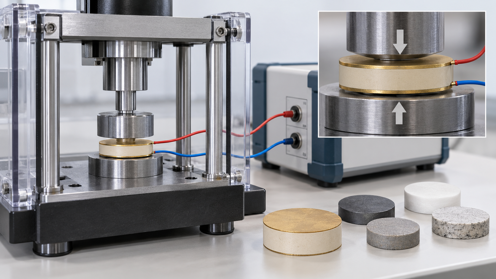
- What piezoelectric materials are (the short version)
- How they work — polarization, the perovskite structure, the morphotropic phase boundary
- Reading the metrics — d33, d31, g33, coupling factors, Qm, Curie temperature
- The material families — PZT, single crystals, KNN, BNT, BaTiO 3 -based, PVDF, AlN/ScAlN
- Why the numbers change with measurement conditions
- Lead-free regulation — the RoHS exemptions
- Our calculations: d33 × g33, a working-temperature guide, lead and niobium
- Applications, and where lead-free stands today
- Limits, and what could not be confirmed
- How to read evaluations and standards
- Glossary
- References (primary sources)
- Claim-to-source audit
Sourced = stated in published material (link given)
Our calculation = a figure this article derived, with the assumptions spelled out
Not yet confirmed = a plan or schedule whose outcome has not been confirmed
Materials-design interpretations are marked separately as Commentary. Inference is shown in bold.
Values such as d33 and the Curie temperature quoted here differ by source in sample form (sintered body, single crystal, thin film, film), measurement method and temperature. A manufacturer’s stated value is a typical value under that company’s conditions, not a guaranteed value for production parts. Please do not read laboratory champion data as the performance of production parts. This article does not rank materials or companies, and gives no individual advice on medical devices or safety.
1. What piezoelectric materials are (the short version)
- Piezoelectricity converts force into electricity and back: force produces charge (the direct effect), and a voltage changes the shape (the converse effect). The size of this conversion is expressed by piezoelectric constants such as d33
- Why PZT has been the mainstream, and its weak point: PZT has a large d33 and its properties can be tuned through composition. It also contains more than 60% lead by weightSourced [Ref. 1]. The EU RoHS Directive restricts lead strictly, but PZT piezoceramics are covered by an exemptionSourced [Ref. 14]
- Going lead-free is not just “finding a material with the same number”: compositions with a large d33 tend to have a low Curie temperature, and sintering and reliability raise separate problems. Several reviews judge that lead-free materials are at the stage of being usable for particular applications, not of broadly replacing PZTSourced [Refs. 2, 3, 4]
A d33 value is a different thing depending on the material form (sintered body, single crystal, thin film, polymer), the measurement method (quasi-static, resonance, large field) and the poling conditions. When a lead-free d33 is placed next to PZT, look at the Curie temperature (or depolarization temperature) and the measurement conditions together.
2. How they work — polarization, the perovskite structure, the morphotropic phase boundary
A piezoelectric material is one in which the centres of positive and negative charge in the crystal are displaced, that is, the crystal is polarized. When force deforms the crystal, the polarization changes and charge appears on the surface (the direct effect). Conversely, a voltage deforms the crystal (the converse effect). PZT, BaTiO3, KNN and BNT have the ABO3 perovskite structure, and the polarization is usually explained as arising when the B-site ion sits slightly off centre (a general explanation; this is the article’s commentary).
In a sintered ceramic the polarization directions of the grains are not aligned, so the piezoelectric response is small as it stands. A treatment called poling, in which a high electric field aligns the directions, is applied (commentary). PI Ceramic states that its data were measured 24 to 48 hours after poling at 23 °CSourced [Ref. 8]. The later sections show how measured values move with poling conditions.
The idea used to explain a high d33 is the morphotropic phase boundary (MPB). Liu and Ren describe, for the Ba(Ti0.8Zr0.2)O3–(Ba0.7Ca0.3)TiO3 (BZT–BCT) system, an MPB that starts from a triple point of cubic, rhombohedral and tetragonal phases; at MPB compositions the polarization can rotate easily between the tetragonal <001> and rhombohedral <111> directions, which is why d33 is largeSourced [Ref. 7]. PZT and PMN–PT are said to have a similar triple point [Ref. 7].
3. Reading the metrics — d33, d31, g33, coupling factors, Qm, Curie temperature
| Metric | Meaning | Reading note |
|---|---|---|
| d33 (pC/N, 10−12 C/N) | Charge generated per unit force applied in the same direction. Saito et al. define it as “the induced charge per unit force applied in the same direction” [Ref. 1]. For the converse effect the same value can be expressed as strain per unit field (m/V, pm/V) (commentary) | Changes with poling conditions, measurement method, temperature and sample form. For BZT–BCT the value spans 560–620 pC/N depending on poling conditions [Ref. 7] |
| d31 | Coefficient for a direction perpendicular to the force. Relevant to the bending and lateral vibration of plate-shaped elements | The sign depends on the axis convention and on the material. PZT is listed with positive d33 and negative d31 [Ref. 8]; PVDF film is listed with positive d31 and negative d33 [Ref. 9]. When comparing, check the absolute values and the axes |
| g33 (10−3 V·m/N) | Electric field generated per unit applied stress; it expresses the voltage-output sensitivity. g is d divided by the permittivity (an explanation based on the definition) | A large d33 does not give a large g if the permittivity is also large. PIC153, with a high permittivity, has a d33 of 600 pC/N but a g33 of 16.4, smaller than the 25 of PIC255 [Ref. 8] |
| kp, kt, k31, k33 (coupling factors) | Dimensionless coefficients that express the efficiency of conversion between electrical and mechanical energy | Different values for each vibration mode (spreading of a disc, thickness, length of a bar and so on). PIC255 has kp 0.62 and k33 0.69; the BNT-type PIC700 has kp 0.14 and k33 0.43 [Ref. 8] |
| Qm (mechanical quality factor) | Expresses how small the mechanical loss is at resonance. Larger means less loss | The hard PZT PIC181 is 2,000 and the soft PIC255 is 80 [Ref. 8]. Hard types with a large Qm are used for high-power applications with large voltages and currents (as described by PI Ceramic [Ref. 22]) |
| Relative permittivity, tanδ | Properties as a capacitor. tanδ is the dielectric loss | PIC255 has εT33/ε0 of 1,800 and tanδ of 20×10−3; PIC181 has 1,200 and 3×10⁻³ [Ref. 8]. These are low-frequency small-signal values and change with frequency and field (commentary) |
| Curie temperature Tc / depolarization temperature Td | Tc is the temperature at which ferroelectricity is lost. For BNT-type materials the manufacturer’s document lists a depolarization temperature rather than Tc (in general, the depolarization temperature is lower than Tc and is used as a guide to where the piezoelectric response begins to fall: commentary) | In PI Ceramic’s document the “190 °C” for PIC700 is a depolarization temperature [Ref. 8]. Do not read it as the same thing as a “Tc” in the same table. The manufacturer’s recommended operating temperature is up to 50% of Tc [Ref. 8] |
| e31,f (C/m2) | Transverse piezoelectric stress constant used for thin films clamped on a substrate | A film is constrained by its substrate, so this is an index different from the bulk d31. A review gives the expression relating e31,f to d31 and the elastic compliances [Ref. 11] |
All Sourced (PI Ceramic [Ref. 8], Measurement Specialties [Ref. 9], Saito et al. [Ref. 1], Liu and Ren [Ref. 7], Jung et al. [Ref. 11]). Parts marked “commentary” are this article’s explanations based on general definitions.
4. The material families — PZT, single crystals, KNN, BNT, BaTiO3-based, PVDF, AlN/ScAlN
The table below lists, for each family, typical values confirmed in primary sources together with their conditions. Sample forms, measurement methods and sources all differ, so the table is not meant to rank the materials.
| Family | Sample form | Values confirmed, and conditions | Source |
|---|---|---|---|
| Soft PZT (PIC151, PIC255, PIC153 and others) | Sintered body (manufacturer’s stated values) | PIC255: Tc 350 °C, d33 400 pC/N, εT33/ε0 1,800. PIC151: Tc 250 °C, d33 500, εT33/ε0 2,500. PIC153: Tc 160 °C, d33 600, εT33/ε0 4,500. Across the five soft types: d33 240–600 pC/N, Tc 160–350 °C. 23 °C, test pieces of the EN 50324-2 shape, 24–48 h after poling | [8] |
| Hard PZT (PIC181 and others) | Sintered body (manufacturer’s stated values) | PIC181: Tc 330 °C, d33 265 pC/N, εT33/ε0 1,200, tanδ 3×10⁻³, Qm 2,000. Across the five hard types: d33 190–300 pC/N, Tc 270–370 °C. Same conditions as above | [8] |
| PZT-type thin films | Film on a substrate | |e31,f| about 12.2–15.3 C/m2 for PZT-type films. Crystallization needs 500–700 °C (a review’s statement) | [11] |
| PMN–PT and PZN–PT single crystals | Single crystal (<001>-oriented rhombohedral) | Reported d33 above 2,500 pC/N, k33 above 90% and dielectric loss below 1% (1997) | [5] |
| Sm-doped PMN–PT | Ceramic | d33 up to 1,500 pC/N, ε33/ε0 above 13,000, Tc 89 °C | [6] |
| KNN-type | Textured ceramic (paper), sintered body (manufacturer) | Saito et al. (2004): d33 above 300 pC/N, up to 416 pC/N when textured. PI Ceramic PIC753: Tc 300 °C, d33 241 pC/N, kp 0.53, Qm 200 (preliminary data). PIC758 is annotated as under development with no specifications | [1] [8] |
| BNT-type | Sintered body (manufacturer) | PIC700: depolarization temperature 190 °C, d33 100 pC/N, kp 0.14, tanδ 30×10−3 (preliminary data) | [8] |
| BZT–BCT | Ceramic | d33 of 560–620 pC/N (a range depending on poling conditions; 20 °C; Berlincourt-type d33 meter), Tc 93 °C, relative permittivity about 3,060. Sintered at 1,450–1,500 °C in air | [7] |
| PVDF and copolymer films | Stretched polymer film | PVDF: d31 23, d33 −33 pC/N, εr 12–13, g31 216×10−3 V·m/N. Copolymer: d31 11, d33 −38. Use or storage above 100 °C is not recommended for PVDF, and the copolymer is rated to 135 °C at most (a 1999 manufacturer document) | [9] |
| AlN and ScAlN thin films | Sputtered film | |e31,f| about 1.1 C/m2 for AlN and about 3.2 C/m2 for ScAlN (Sc fraction x ≈ 0.41, a value for the ferroelectric state). Deposition below 400 °C, compatible with CMOS processing (a review’s statement) | [11] |
All Sourced. Manufacturer values are typical values for sintered bodies and include preliminary data. The “Sc fraction x ≈ 0.41” value follows the table note in the review [Ref. 11].
PI Ceramic says that its BNT-type and KNN-type lead-free materials sit at various levels of technological maturity and are supplied for custom application development, and that lead-free piezoceramics can be an alternative to lead-containing ones especially in resonant applications. At the same time, lead-free materials behave differently from PZT in applications, so parameters and dimensions usually have to be adjusted for each application and long-term stability retestedSourced [Ref. 22]. The lead-free columns of its material data carry the note that reliability must be re-evaluated in each application [Ref. 8].
The reviews agree. In 2009 Rödel et al. wrote that the new materials appear adequate in specific but narrow application ranges but are not yet suited to replace PZT on a broader basis [Ref. 2]; in 2015 that there are now clear prospects for transfer into applications in some areas, while demanding applications needing high reliability, large displacement, high frequency and a wide temperature range appear to remain in the distant future [Ref. 3]. Hong et al. (2016) note that commercial products for certain applications have appeared, but that the goal of a lead-free piezoceramic equivalent or superior to PZT does not seem to have been fulfilled yet [Ref. 4].
In Fig. 3, the points with a large d33 (1,500 pC/N for Sm-doped PMN–PT and 620 pC/N for BZT–BCT) both sit on the low-Tc side, at around 90 °CSourced [Refs. 6, 7]. PIC255, with a Tc of 350 °C, has a d33 of 400 pC/N [Ref. 8]. Liu and Ren point out, however, that the high d33 of BZT–BCT cannot be explained by the low Tc alone, because existing lead-free materials with a similar Tc show much lower d33 [Ref. 7].
In KNN-type materials too, lowering the temperature of the orthorhombic–tetragonal polymorphic transition toward room temperature raises the room-temperature properties, but this usually comes at the expense of a lower TcSourced [Ref. 10]. Liu and Ren also report that d33 of BZT–BCT peaks at the temperature where the sample crosses the MPB [Ref. 7], and Dwivedi et al. state that the phase coexistence in KNN–BZT depends strongly on temperature, unlike the classic MPB of PZT [Ref. 10]. From a materials viewpoint, choosing a lead-free material by its room-temperature maximum d33 alone means its performance will move at the operating temperature. Besides the room-temperature values in the table, the change of d33 over the operating temperature range has to be checked (this article’s commentary).
A review states that KNN is hard to densify into a ceramic with good electrical properties by conventional sintering because the alkali elements (K, Na) are highly volatileSourced [Ref. 10]. BZT–BCT was made with calcination at 1,350 °C and sintering at 1,450–1,500 °C [Ref. 7]. For thin films, another review states that the lead in PZT is a contamination source for CMOS processes, while KNN also needs crystallization at 600 °C or above and its mobile K+ and Na+ ions pose a contamination riskSourced [Ref. 11]. In short, going lead-free is not only a change of composition but a replacement of the whole process: powders, firing atmosphere, electrodes, deposition tools and line control (this article’s commentary).
5. Why the numbers change with measurement conditions
Even a single “d33” is a different quantity under a different condition when it comes from the quasi-static method, the resonance method, strain at a large field, or a thin-film measurement. The figure below sorts out the measurement differences met in this article.
The review by Damjanovic (Rep. Prog. Phys. 1998) discusses how polarization switching and domain-wall displacement contribute to the dielectric and piezoelectric properties of ferroelectric ceramics and thin filmsSourced [Ref. 21]. Domain-wall motion can depend on field and frequency, so a coefficient measured at small signal is not necessarily the same as the effective value when the part is driven at a large field (this article’s commentary).
For the quasi-static method (the d33 meter), the guide from the UK National Physical Laboratory (NPL, 2001) describes a quasi-static measurement at a few hundred hertz in which a small oscillating force is applied and the output charge is divided by the force amplitude. It advises checking the static pre-load, the AC load level, the sample thickness, the measurement frequency, the calibration, the temperature, and moisture and air currents, because they affect the resultSourced [Ref. 23]. The same guide says the resonance method is the most reliable, but needs a sample whose shape gives a pure fundamental resonance mode. At the time of that guide, there was no standard for the quasi-static method.
Typical misreadings
- Different forms: single crystals (d33 above 2,500 pC/N [Ref. 5]), ceramics, thin films (described by e31,f [Ref. 11]) and polymers (d33 of −33 pC/N [Ref. 9]) cannot be compared by putting them in one table
- Tc versus Td: the “190 °C” for the BNT type in the manufacturer’s document is a depolarization temperature [Ref. 8]. Do not read it in the same sense as the numbers in the Tc column
- Preliminary data: PIC753 and PIC700 are preliminary data that the manufacturer says may change [Ref. 8]. Do not write laboratory or prototype-stage values as the performance of production parts
- The comparison target: when Liu and Ren say “similar to PZT”, the PZT is the ultrasoft PZT-5H (d33 about 590 pC/N) [Ref. 7], not PZT in general. When something is described as “on a par with PZT”, check which PZT
6. Lead-free regulation — the RoHS exemptions
The EU RoHS Directive (Directive 2011/65/EU) restricts certain hazardous substances in electrical and electronic equipment. The limit for lead is 0.1% by weight in a homogeneous materialSourced [Ref. 14]. PZT contains more than 60% lead by weight [Ref. 1], so it far exceeds this limit (calculated in the next section). Whether PZT piezoceramics can be used in electrical and electronic equipment therefore rests on the exemptions in Annex III.
Commission Delegated Directive (EU) 2025/2363, adopted on 8 September 2025, revised the exemptions for lead in glass or ceramic as followsSourced [Ref. 14].
| Annex III entry | Scope (summary of the text) | Expiry |
|---|---|---|
| 7(c)-I | Electrical and electronic components containing lead in a glass or ceramic other than dielectric ceramic in capacitors, e.g. piezoelectronic devices, or in a glass or ceramic matrix compound. All categories | 30 June 2027 |
| 7(c)-VI (new) | Lead in a ceramic that fulfils either of these functions: (1) use in piezoelectric lead zirconium titanate (PZT) ceramics, (2) providing ceramics with a positive temperature coefficient (PTC). All categories (except applications covered by points 7(c)-II, 7(c)-III and 7(c)-IV and by point 14 of Annex IV) | 31 December 2027 |
| 7(c)-II | Lead in dielectric ceramic in capacitors for a rated voltage of 125 V AC or 250 V DC or higher | 31 December 2027 |
All Sourced (Annex of Delegated Directive (EU) 2025/2363 [Ref. 14]). Entry 7(c)-V (lead in glass applications) is omitted.
The recitals of the same directive give the conclusions of the evaluationSourced [Ref. 14]. In ceramics, lead provides dielectric, piezoelectric, pyroelectric, ferroelectric and other properties over a wide range of temperatures, voltages and frequencies. Substitutes for lead-containing ceramics and glasses are either not technically practicable for all applications or not sufficiently reliable for specific applications. Entry 7(c)-I was renewed only for a short term, and its expiry was set to one date for all categories.
Delegated Directive (EU) 2025/2363 was adopted on 8 September 2025 and published in the Official Journal on 21 November 2025. It enters into force on the twentieth day after publication (as written in its text), which by our calculation is 11 December 2025. Member States must adopt the national measures by 30 June 2026 and apply them from 1 July 2026 (as of the checking date of 10 October 2026, that date has passed). We have not checked the state of each country’s national law. The expiry dates of 7(c)-I (30 June 2027) and of 7(c)-VI and 7(c)-II (31 December 2027) are future datesNot yet confirmed, and we could not confirm whether renewal requests have been filed or what applies afterwards. The RoHS Directive covers electrical and electronic equipment; other legislation (such as REACH) and non-EU regulation are outside this article.
7. Our calculations: d33 × g33, a working-temperature guide, lead and niobium
(1) The product of d33 and g33 — “large d33” and “large voltage output” are different things
We multiply d33 and g33 from the manufacturer’s documentsOur calculation. The unit is 10−12 C/N × 10−3 V·m/N = 10−15 m2/N, shown converted to 10−12 m2/N.
- Soft PZT: PIC151 is 500 × 21.5 = 10,750 → 10.8, PIC255 is 400 × 25 = 10,000 → 10.0, PIC153 is 600 × 16.4 = 9,840 → 9.8 [Ref. 8]
- Hard PZT: PIC181 is 265 × 23 = 6,095 → 6.1 [Ref. 8]
- Lead-free (preliminary data): KNN-type PIC753 is 241 × 20.0 = 4,820 → 4.8; BNT-type PIC700 is 100 × 16 = 1,600 → 1.6 [Ref. 8]
- PVDF film: 33 × 330 = 10,890 → 10.9 (absolute values of d33 −33 pC/N and g33 −330×10−3 V·m/N, from a 1999 manufacturer document [Ref. 9])
Assumptions and limits: this is a product of static, small-signal material constants and excludes the coupling factor, mechanical impedance, operating frequency, element shape and load. The PZT and KNN/BNT values come from one manufacturer’s August 2024 document and the PVDF value from another manufacturer’s 1999 document, so editions and conditions differ. The product is not a value that ranks output or sensitivity. Even so, it shows that PIC153 (600 pC/N), the soft PZT with the largest d33, gives a smaller product than PIC151 and PIC255. Because g is d divided by permittivity, the product is proportional to d squared divided by permittivity, so a high-permittivity material has trouble raising its material index for output even if d33 is large (this article’s commentary).
(2) A working-temperature guide — applying the manufacturer’s “50% of Tc”
PI Ceramic’s document gives the recommended operating temperature as “up to 50% of the Curie temperature” [Ref. 8]. We apply this by multiplying the Tc value (in °C) in the document by 0.5Our calculation.
- PIC255: 350 × 0.5 = 175 °C. PIC181: 330 × 0.5 = 165 °C. PIC151: 250 × 0.5 = 125 °C. PIC153: 160 × 0.5 = 80 °C
- KNN-type PIC753: 300 × 0.5 = 150 °C. BNT-type PIC700: depolarization temperature 190 × 0.5 = 95 °C
Assumptions and limits: the document does not state the temperature basis of “50%” (Celsius or absolute), so we multiplied the Celsius value. The guide applies only to PI Ceramic’s materials and does not apply to other makers’ materials, to actual guaranteed temperatures, or to the voltages and durations of use. The BNT type uses the depolarization temperature instead of Tc. Even so, the guide for PIC153, with the large d33 (Tc 160 °C), is less than half that of PIC255, with the smaller d33 (Tc 350 °C), which agrees with the trend in Fig. 3 that “large d33” and “usable at high temperature” tend to trade off.
(3) Lead content and the RoHS limit
The lead in PZT is above 60% by weight [Ref. 1] and the RoHS limit is 0.1% in a homogeneous material [Ref. 14]. 60 ÷ 0.1 = 600 times or moreOur calculation.
Assumptions and limits: 60% is the statement in Saito et al.’s paper (“more than 60 weight per cent”) and not an exact value for each composition. The 0.1% limit is judged per homogeneous material, not as an average over the whole part. Even so, the size of this gap is why the use of PZT depends on an exemption (this article’s commentary).
(4) Raw material for lead-free materials — niobium supply
According to the USGS Mineral Commodity Summaries 2026, world mine production of niobium in 2025 (estimated) was 112,000 t (niobium content), of which Brazil produced 104,000 t [Ref. 13]. 104,000 ÷ 112,000 = about 92.9%Our calculation. Ibn-Mohammed et al. point out that KNN contains about 60 wt% Nb2O5 [Ref. 12]. Niobium is 69.904% of Nb2O5 by weight (USGS footnote), so 60% × 0.699 = about 42% NbOur calculation.
Assumptions and limits: “about 60 wt%” is the paper’s approximate figure and varies with composition (Li, Ta, Sb additions and so on). USGS gives the breakdown of US niobium consumption as about 77% steels and about 23% superalloys [Ref. 13]. We have not checked how demand from piezoceramics would affect supply.
Ibn-Mohammed et al. question the view of KNN as a “less hazardous” substitute. Nb2O5 is much less toxic to humans than lead oxide, they say, but its mining and extraction cause significant environmental damageSourced [Ref. 12]. In USGS statistics, most niobium mine production is concentrated in one country [Ref. 13]. Which material counts as “better” changes with the axis chosen: toxicity to humans, mining burden, concentration of supply, or treatment after use. From a materials viewpoint, the discussion of going lead-free needs to separate reducing the regulated substance from reducing the environmental burden over the whole life cycle (this article’s commentary).
8. Applications, and where lead-free stands today
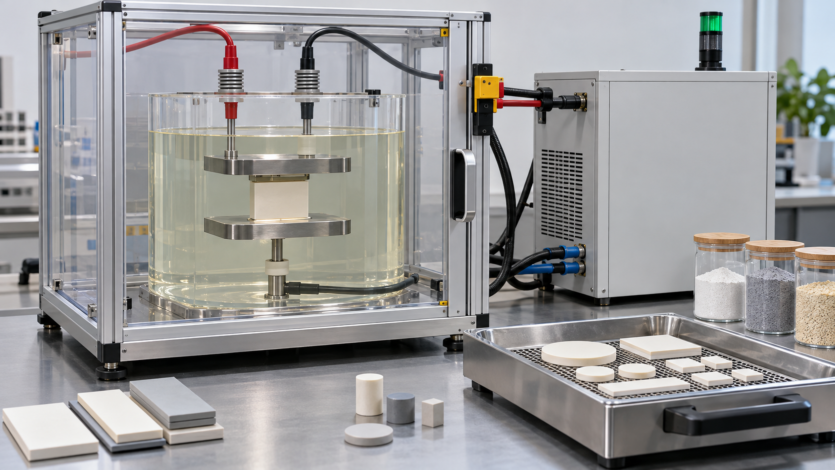
Ultrasonics, sensors and actuators
PI Ceramic lists, for soft PZT, actuators for micro- and nano-positioning, vibration sensors, ultrasonic transmitters and receivers for flow and level measurement, and electro-acoustic transducers. Hard PZT is described as used in high-power ultrasonics, where large electrical and mechanical loads are applied (cleaning, material processing, dispersing liquids), and in sonarSourced [Ref. 22]. For its lead-free BNT and KNN types, the company says an alternative is possible especially in resonant applications, and that first positive development results can be demonstrated for micropumps, ultrasonic nebulizers, power ultrasonic transducers and sensors [Ref. 22]. Its application table lists air-bubble detection, flow metering, mixing and dispersion, and sonication (this article does not address the performance or safety of any medical use).
MEMS and thin films
The review by Jung et al. states that the most widely used piezoelectric material in MEMS is PZT (d33 of 200–600 pC/N), used for example in MEMS mirrors for LiDAR, but that it needs 500–700 °C for crystallization, which raises compatibility with CMOS processes, a lead contamination risk, and hysteresis associated with ferroelectricitySourced [Ref. 11]. AlN has a smaller piezoelectric constant but can be deposited below 400 °C, is compatible with CMOS and shows no hysteresis. Adding Sc to give ScAlN is summarized as raising e31,f to about 3.2 C/m2 (x ≈ 0.41) [Ref. 11]. The measurement of thin films is specified in IEC 62047-30 and JIS C 5630-30 [Refs. 15, 16].
Polymer films
The manufacturer’s manual explains that the acoustic impedance of PVDF film is about one tenth that of PZT (PVDF 2.7 and PZT 30, in units of 106 kg/m2·s), close to that of water and living tissueSourced [Ref. 9]. It also says that a piezo film is a relatively weak transmitter compared with ceramics, particularly at resonance and at low frequencies, and that the film suits strain sensing needing wide bandwidth and high sensitivity [Ref. 9].
Where lead-free stands today
On the basis of a figure-of-merit analysis, Rödel et al. conclude that lead-free piezoceramics can be envisaged for some applications, while applications demanding reliability, displacement, frequency and temperature range remain far off [Ref. 3]. The 2009 review (adequate in narrow applications) [Ref. 2], the 2016 review (the goal of equalling or exceeding PZT has not been fulfilled) [Ref. 4], and PI Ceramic’s explanation (readjustment for each application and retesting of long-term stability) [Ref. 22] point in the same direction. The text of the directive sets the exemption for lead in PZT piezoceramics until 31 December 2027Sourced [Ref. 14]. This shows that the regulator, too, judged that substitutes are not technically practicable for all applications (a statement in the recitals).
9. Limits, and what could not be confirmed
(1) Texts of the standards
We have not checked the texts of ISO 19622, 21819, 17859 and 5712, IEC 60483 and 62047-30, IEEE 176, EN 50324-2, and JIS R 1696, R 1699, R 1682, R 1762 and C 5630-30 (we checked the titles and scopes shown on the ISO, IEC and JSA pages). Test conditions, procedures and acceptance criteria are not given.
(2) Reliability and life of lead-free materials
Fatigue, aging in heat and humidity, and the scatter of production characteristics of lead-free materials are not given numerically in the primary sources we could confirm. PI Ceramic’s documents also say reliability must be re-evaluated for each application [Refs. 8, 22].
(3) PVDF values
The d31 and d33 of PVDF are typical values from Measurement Specialties’ 1999 manual. We have not checked current editions or values for other makers and stretching conditions.
(4) Scope of regulation
We could not confirm what applies after the expiry of the RoHS exemptions (whether renewal requests were filed, and the Commission’s decision). Non-EU regulation, REACH and the state of national transposition are not covered.
(5) ASTM, and a JIS or ISO for the room-temperature resonance method
We could not find an applicable ASTM standard for piezoceramics in non-ASTM sources (the ASTM site was not opened). We also found no JIS or ISO specifying the room-temperature resonance method (Chapter 10).
(6) Market and shipment volumes
We could not confirm public statistics on the adoption or shipment volumes of lead-free materials, so none are given.
- d33 is a number with conditions. It differs between sintered bodies, single crystals, thin films and polymers, and also moves with poling conditionsSourced
- Compositions with a large d33 tend to have a low Tc. Sm-doped PMN–PT has a d33 of up to 1,500 pC/N at a Tc of 89 °C, and BZT–BCT 560–620 pC/N at a Tc of 93 °CSourced
- Lead-free materials are at the stage of being usable in particular applications. The manufacturer asks for readjustment for each application and retesting of long-term stability, and reviews say demanding applications are far offSourced
- The EU sets the exemption for lead in PZT piezoceramics until 31 December 2027. 7(c)-I runs to 30 June 2027Sourced. What applies afterwards is not confirmedNot yet confirmed
- “Lead-free” does not always mean “environmentally friendly.” KNN contains about 60 wt% Nb2O5, and about 93% of niobium mine production is in BrazilSourced / Our calculation
10. How to read evaluations and standards
The performance of a piezoelectric material is measured through these quantities: d33 and d31 (the relation between force and charge, or between field and strain), g33 (voltage-output sensitivity), the coupling factor k, the mechanical quality factor Qm, relative permittivity, dielectric loss tanδ and the Curie temperature Tc. For ceramics, two approaches are common: obtaining many coefficients from the small-signal electrical impedance near the resonance and antiresonance frequencies of a test piece of defined shape (disc, bar and so on), and the quasi-static method (the d33 meter), which applies a small oscillating force and measures the charge. Strain at a large field, behaviour at high temperature and high load, and power generation have separate methods, and for thin films the electromechanical conversion is measured with the film clamped on its substrate.
In this survey we confirmed that ISO/TC 206 (fine ceramics) and JIS standards drafted by the Japan Fine Ceramics Association include several measurement standards for piezoceramics. We could not confirm an applicable ASTM standard.
| Item evaluated | ISO | IEC / IEEE (and regional) | JIS | ASTM | What changes the value |
|---|---|---|---|---|---|
| d33 by the quasi-static method (d33 meter, Berlincourt method) Sourced | ISO 19622:2018, “Fine ceramics (advanced ceramics, advanced technical ceramics) — Test method for piezoelectric constant d33 of piezoelectric ceramics by direct quasi-static method” (Edition 1, April 2018; confirmed at review in 2023) [Ref. 24] | Could not be confirmed | JIS R 1696:2014, test method for the piezoelectric constant d33 of piezoelectric ceramics by the quasi-static direct piezoelectric effect method (title translated by us) [Ref. 28] | Could not be confirmed | Pre-load, AC load level, sample thickness, frequency, calibration, temperature (NPL guide [Ref. 23]). Poling conditions |
| Small-signal properties of piezoceramics (resonance method: coupling factors, d, g, elastic constants, Qm and so on) Sourced | Could not be confirmed | IEC 60483:1976, “Guide to dynamic measurements of piezoelectric ceramics with high electromechanical coupling” (IEC/TC 49) [Ref. 17] IEEE Std 176-1987, “IEEE Standard on Piezoelectricity” (withdrawn on 6 March 2000) [Ref. 19] EN 50324-2, “Piezoelectric properties of ceramic materials and components – Part 2: Methods of measurement – Low power” (CENELEC regional standard, 2002 edition) [Ref. 20] | Could not be confirmed (we found no JIS specifying the room-temperature resonance method in the range searched) | Could not be confirmed | Test-piece dimensions, time since poling, temperature, small voltage. PI Ceramic’s values are for “test pieces of EN 50324-2 dimensions, 24–48 h after poling, 23 °C” [Ref. 8] |
| Piezoelectric properties at high load and high temperature Sourced | ISO 21819-1:2018 (resonance/antiresonance method, high-temperature conditions) and ISO 21819-2:2018 (electrical transient response method, high vibration levels). Both Edition 1, August 2018, confirmed at review in 2024 [Refs. 25, 26] | Could not be confirmed | JIS R 1699-1:2016 and JIS R 1699-2:2016 (same subject as the ISO titles; titles translated by us) [Refs. 29, 30] | Could not be confirmed | Temperature and vibration level. The range of each method is set by the standard (texts not checked) |
| Field-induced strain at a high electric field Sourced | ISO 17859:2015, “Measurement method of piezoelectric strain at high electric field” (Edition 1, September 2015; confirmed in 2020; shown as under review on the ISO page on 10 October 2026). Scope: applied field 0–2 MV/m, field frequency 0.1–1 Hz [Ref. 27] | Could not be confirmed | JIS R 1682:2007, measurement method of field-induced strain of fine ceramics at high electric field (title translated by us) [Ref. 31] | Could not be confirmed | Field magnitude and frequency, and how the sample is held. Not guaranteed to equal the small-signal d33 |
| Electromechanical conversion of MEMS piezoelectric thin films Sourced | Could not be confirmed | IEC 62047-30:2017, “Semiconductor devices – Micro-electromechanical devices – Part 30: Measurement methods of electro-mechanical conversion characteristics of MEMS piezoelectric thin film” (Edition 1, 15 September 2017) [Ref. 15]. Parts 36 (2019) and 37 (2020) of the same series cover environmental tests (titles only checked) [Ref. 15] | JIS C 5630-30:2020, Micromachines and MEMS — Part 30: Measurement method of electromechanical conversion characteristics of MEMS piezoelectric thin film (title translated by us). Identical (IDT) to IEC 62047-30:2017 [Ref. 16] | Could not be confirmed | Substrate, film thickness, electrodes, field, frequency. The standard defines the method and the report format (IEC scope statement [Ref. 15]) |
| Power generation of piezoelectric resonant devices (energy harvesting) Sourced | ISO 5712:2022, “Method for measuring the power generation characteristics of piezoelectric resonant devices for stand-alone power sources” (Edition 1, May 2022) [Ref. 32] | Could not be confirmed | JIS R 1762:2020, fine ceramics — method for measuring power generation characteristics of piezoelectric devices for stand-alone power sources (title translated by us) [Ref. 33] | Could not be confirmed | Vibration frequency and acceleration, and load. See our explainer on energy harvesting |
| Terminology for piezoceramics Sourced | Could not be confirmed | IEC TS 61994-4-2:2011, “…Glossary – Part 4-2: Piezoelectric and dielectric materials – Piezoelectric ceramics” (Edition 2.0, technical specification, 8 March 2011) [Ref. 18] | Could not be confirmed | Could not be confirmed | A definition of terms; it does not set measurement conditions (as far as the title shows) |
| Summary (our own) Our calculation | How the standards are positioned: ISO 19622, 21819, 17859 and 5712 are international standards, all handled by ISO/TC 206. JIS R 1696, R 1699, R 1682 and R 1762 are national standards drafted by the Japan Fine Ceramics Association; the “corresponding international standard” field on the JSA page shows no international standard (we could not confirm an identical (IDT) relationship), and their establishment years are earlier than the ISO ones (R 1696 in 2014, ISO 19622 in 2018). For MEMS thin films IEC 62047-30 is the international standard and JIS C 5630-30 is its identical national standard. IEC 60483 dates from 1976, IEEE 176-1987 is withdrawn, and EN 50324-2 is a European regional standard that a manufacturer cites for its test-piece dimensions as a working reference. | ||||
Because the texts are paid, we keep to number, title, year of issue and scope (as stated on the ISO and JIS pages). ASTM International’s site states that AI use is not permitted, so we did not open it. We found no applicable ASTM standard for piezoceramics in the non-ASTM sources searched (ISO, JIS, NPL, papers).
Notes on reading standards
- A standard is a test method, not a guarantee of material performance. PI Ceramic’s values are described as typical values measured on test pieces with the dimensions of EN 50324-2 [Ref. 8]. A standard exists to make measurements comparable; it does not guarantee that the value will appear in your element or under your operating conditions
- The same property name can mean different methods and different standards. d33 by the quasi-static method (ISO 19622), by resonance, by strain at a high field (ISO 17859) and on a thin film (IEC 62047-30) differ in both conditions and standards (Chapter 5). The NPL guide (2001) noted that the quasi-static method then had no standard, and that each system performed the measurement slightly differently [Ref. 23]. JIS R 1696 (2014) and ISO 19622 (2018) were established later. For an older d33, check which procedure it came from
- Read a manufacturer’s value together with its standard, edition and conditions. PI Ceramic’s example lists the document edition (August 2024), the time since poling (24–48 hours), the temperature (23 °C) and the test-piece standard (EN 50324-2) [Ref. 8]. A note that data are preliminary, or that a material is under development with no specification, matters as much as the standard value
- Watch for old, withdrawn and under-review standards. IEEE 176-1987 is withdrawn [Ref. 19], IEC 60483 is a 1976 guide, and ISO 17859 is under review [Ref. 27]Not yet confirmed. Whether the premises of an old standard fit a new material (lead-free ceramics, ScAlN films) is to be checked by comparing the text of the standard with the conditions of the material (this article’s commentary)
11. Glossary
- Direct / converse piezoelectric effect
- Charge appears under force / the shape changes under voltage.
- Polarization / poling
- Displacement of the charge centres / aligning the polarization with a high electric field.
- d33, d31
- Piezoelectric constants: along the force direction (33) and perpendicular to it (31). Unit pC/N.
- g33
- Piezoelectric voltage constant: field per unit stress. Unit 10−3 V·m/N.
- Coupling factor k
- Expresses the efficiency of electrical-to-mechanical energy conversion.
- Qm
- Mechanical quality factor: how small the loss is at resonance.
- Curie temperature Tc
- The temperature at which ferroelectricity is lost.
- Depolarization temperature Td
- A guide to the temperature where polarization starts to be lost; used in BNT-type documents.
- MPB
- Morphotropic phase boundary: where two ferroelectric phases meet as the composition changes.
- PZT
- Lead zirconate titanate, the representative lead-containing piezoceramic.
- KNN / BNT
- Potassium sodium niobate / bismuth sodium titanate: lead-free material systems.
- BZT–BCT
- Ba(Ti,Zr)O3–(Ba,Ca)TiO3, a lead-free perovskite system.
- PVDF
- Polyvinylidene fluoride, a polymer made piezoelectric by stretching and poling.
- e31,f
- Transverse piezoelectric stress constant of a film clamped on a substrate. Unit C/m2.
- RoHS exemption
- A mechanism listed in Annex III that allows a restricted substance in specific uses, for a limited period.
12. References (primary sources)
- Saito Y. et al. “Lead-free piezoceramics”, Nature 432, 84–87 (2004), DOI 10.1038/nature03028 — doi.org/10.1038/nature03028
- Rödel J. et al. “Perspective on the Development of Lead-free Piezoceramics”, J. Am. Ceram. Soc. 92, 1153–1177 (2009), DOI 10.1111/j.1551-2916.2009.03061.x — doi.org/10.1111/j.1551-2916.2009.03061.x
- Rödel J. et al. “Transferring lead-free piezoelectric ceramics into application”, J. Eur. Ceram. Soc. 35, 1659–1681 (2015), DOI 10.1016/j.jeurceramsoc.2014.12.013 — doi.org/10.1016/j.jeurceramsoc.2014.12.013
- Hong C.-H. et al. “Lead-free piezoceramics – Where to move on?”, J. Materiomics 2, 1–24 (2016), DOI 10.1016/j.jmat.2015.12.002 (open access) — doi.org/10.1016/j.jmat.2015.12.002
- Park S.-E., Shrout T. R. “Ultrahigh strain and piezoelectric behavior in relaxor based ferroelectric single crystals”, J. Appl. Phys. 82, 1804–1811 (1997), DOI 10.1063/1.365983 — doi.org/10.1063/1.365983
- Li F. et al. “Ultrahigh piezoelectricity in ferroelectric ceramics by design”, Nat. Mater. 17, 349–354 (2018), DOI 10.1038/s41563-018-0034-4 — doi.org/10.1038/s41563-018-0034-4
- Liu W., Ren X. “Large Piezoelectric Effect in Pb-Free Ceramics”, Phys. Rev. Lett. 103, 257602 (2009), DOI 10.1103/PhysRevLett.103.257602 — doi.org/10.1103/PhysRevLett.103.257602
- PI Ceramic GmbH “Piezo Ceramics Material Data” (material data for standard PZT and lead-free materials; August 2024 edition; manufacturer’s stated values) — pi-usa.us …/Piezo_Ceramics_Material_Data.pdf
- Measurement Specialties, Inc. “Piezo Film Sensors Technical Manual”, P/N 1005663-1 REV B (2 April 1999; manufacturer’s stated values) — courses.media.mit.edu/…/MSI-techman.pdf
- Dwivedi S. et al. “Structure, dielectric, and piezoelectric properties of K0.5Na0.5NbO3-based lead-free ceramics”, RSC Adv. 8, 24286–24296 (2018), DOI 10.1039/c8ra04038a (open access) — doi.org/10.1039/c8ra04038a
- Jung Y. et al. “Recent progress in aluminum nitride for piezoelectric MEMS mirror applications: enhancements with scandium doping”, Microsyst. Nanoeng. 11, 179 (2025), DOI 10.1038/s41378-025-01053-8 (open access) — doi.org/10.1038/s41378-025-01053-8
- Ibn-Mohammed T. et al. “Are lead-free piezoelectrics more environmentally friendly?”, MRS Commun. 7, 1–7 (2017), DOI 10.1557/mrc.2017.10 (open access) — doi.org/10.1557/mrc.2017.10
- U.S. Geological Survey “Mineral Commodity Summaries 2026: Niobium (Columbium)” (February 2026) — pubs.usgs.gov/periodicals/mcs2026/mcs2026-niobium.pdf
- European Commission “Commission Delegated Directive (EU) 2025/2363 of 8 September 2025 amending Directive 2011/65/EU … as regards an exemption for lead in glass or ceramic components”, Official Journal L, 21.11.2025 (EUR-Lex) — eur-lex.europa.eu/eli/dir_del/2025/2363/oj/eng
- International Electrotechnical Commission (IEC) “IEC 62047-30:2017” product page (IEC Webstore) — webstore.iec.ch/en/publication/29344
- Japanese Standards Association (JSA) “JIS C 5630-30:2020” standard page (JSA Webdesk; title in Japanese: Micromachines and MEMS — Part 30: Measurement method of electromechanical conversion characteristics of MEMS piezoelectric thin film) — webdesk.jsa.or.jp/books/W11M0090/index/?bunsyo_id=JIS+C+5630-30:2020
- International Electrotechnical Commission (IEC) “IEC 60483:1976” product page (IEC Webstore) — webstore.iec.ch/en/publication/2229
- International Electrotechnical Commission (IEC) “IEC TS 61994-4-2:2011” product page (IEC Webstore) — webstore.iec.ch/en/publication/6261
- IEEE “176-1987 – IEEE Standard on Piezoelectricity” standard page (withdrawn) — standards.ieee.org/ieee/176/356
- AFNOR Editions “NF EN 50324-2 / EN 50324-2:2002” standard page (shows the title and scope of EN 50324-2) — boutique.afnor.org/…/nf-en-503242/…
- Damjanovic D. “Ferroelectric, dielectric and piezoelectric properties of ferroelectric thin films and ceramics”, Rep. Prog. Phys. 61, 1267–1324 (1998), DOI 10.1088/0034-4885/61/9/002 — doi.org/10.1088/0034-4885/61/9/002
- PI Ceramic GmbH “Piezoceramic Materials” (product page; descriptions of soft and hard PZT and lead-free materials and their applications) — piceramic.com/en/products/piezoceramic-materials
- Stewart M., Battrick W., Cain M. (National Physical Laboratory) “Measurement Good Practice Guide No. 44: Measuring Piezoelectric d33 coefficients using the Direct Method”, June 2001 — eprintspublications.npl.co.uk/2768/1/mgpg44.pdf
- International Organization for Standardization (ISO) “ISO 19622:2018 Fine ceramics (advanced ceramics, advanced technical ceramics) — Test method for piezoelectric constant d33 of piezoelectric ceramics by direct quasi-static method” (ISO page) — iso.org/standard/65515.html
- International Organization for Standardization (ISO) “ISO 21819-1:2018 … Characteristic of piezoelectric properties under high-load conditions — Part 1: Resonant-antiresonant method under high-temperature conditions” (ISO page) — iso.org/standard/71874.html
- International Organization for Standardization (ISO) “ISO 21819-2:2018 … Characteristic of piezoelectric properties under high-load conditions — Part 2: Electrical transient response method under high vibration levels” (ISO page) — iso.org/standard/71875.html
- International Organization for Standardization (ISO) “ISO 17859:2015 Fine ceramics (advanced ceramics, advanced technical ceramics) — Measurement method of piezoelectric strain at high electric field” (ISO page) — iso.org/standard/60834.html
- Japanese Standards Association (JSA) “JIS R 1696:2014” standard page (JSA Webdesk; title in Japanese: test method for piezoelectric constant d33 of piezoelectric ceramics by the quasi-static direct piezoelectric effect method) — webdesk.jsa.or.jp/…bunsyo_id=JIS+R+1696:2014
- Japanese Standards Association (JSA) “JIS R 1699-1:2016” standard page (JSA Webdesk; title in Japanese: Fine ceramics — Characteristics of piezoelectric materials under high-load conditions — Part 1: Resonance/antiresonance method under high-temperature conditions) — webdesk.jsa.or.jp/…bunsyo_id=JIS+R+1699-1:2016
- Japanese Standards Association (JSA) “JIS R 1699-2:2016” standard page (JSA Webdesk; title in Japanese: … Part 2: Electrical transient response method under high vibration levels) — webdesk.jsa.or.jp/…bunsyo_id=JIS+R+1699-2:2016
- Japanese Standards Association (JSA) “JIS R 1682:2007” standard page (JSA Webdesk; title in Japanese: Measurement method of field-induced strain of fine ceramics at high electric field) — webdesk.jsa.or.jp/…bunsyo_id=JIS+R+1682:2007
- International Organization for Standardization (ISO) “ISO 5712:2022 Fine ceramics (advanced ceramics, advanced technical ceramics) — Method for measuring the power generation characteristics of piezoelectric resonant devices for stand-alone power sources” (ISO page) — iso.org/standard/81569.html
- Japanese Standards Association (JSA) “JIS R 1762:2020” standard page (JSA Webdesk; title in Japanese: Fine ceramics — Method for measuring power generation characteristics of piezoelectric devices for stand-alone power sources) — webdesk.jsa.or.jp/…bunsyo_id=JIS+R+1762:2020
13. Claim-to-source audit
| Claim in the text | Basis | Type |
|---|---|---|
| PZT contains more than 60% lead by weight. For textured KNN-type ceramics, d33 above 300 pC/N and up to 416 pC/N. The definition of d33 (induced charge per unit force applied in the same direction) | Abstract of Saito et al. (2004) Reference 1 https://doi.org/10.1038/nature03028 | Sourced |
| Lead-free piezoceramics are adequate in specific narrow applications but do not broadly replace PZT (2009). Prospects for transfer in some applications, while demanding applications are far off (2015). Products have appeared for certain applications, but the goal of equalling or exceeding PZT has not been fulfilled (2016) | Abstracts of the three reviews Reference 2 https://doi.org/10.1111/j.1551-2916.2009.03061.x Reference 3 https://doi.org/10.1016/j.jeurceramsoc.2014.12.013 Reference 4 https://doi.org/10.1016/j.jmat.2015.12.002 | Sourced |
| Single crystals of PMN–PT and PZN–PT: d33 above 2,500 pC/N, k33 above 90%, dielectric loss below 1% (<001>-oriented rhombohedral) | Abstract of Park and Shrout (1997) Reference 5 https://doi.org/10.1063/1.365983 | Sourced |
| Sm-doped PMN–PT ceramic: d33 up to 1,500 pC/N, ε33/ε0 above 13,000, Tc 89 °C | Abstract of Li et al. (2018) Reference 6 https://doi.org/10.1038/s41563-018-0034-4 | Sourced |
| BZT–BCT: d33 560–620 pC/N (20 °C, Berlincourt-type meter, a range depending on poling), Tc 93 °C, relative permittivity about 3,060, calcination at 1,350 °C and sintering at 1,450–1,500 °C, dS/dE 1,140 pm/V (PZT 360–900), comparison with PZT-5H (about 590 pC/N), the explanation by the triple point and polarization rotation at the MPB, the remark that Tc alone cannot explain the d33, and d33 peaking at the temperature where the MPB is crossed | Liu and Ren (2009) Reference 7 https://doi.org/10.1103/PhysRevLett.103.257602 | Sourced |
| Soft PZT, five types (d33 240–600 pC/N, Tc 160–350 °C); hard PZT, five types (d33 190–300, Tc 270–370 °C); individual values for PIC255, PIC151, PIC153 and PIC181; values for KNN-type PIC753 and BNT-type PIC700 (preliminary data); PIC758 under development; the BNT temperature is a depolarization temperature; recommended operating temperature up to 50% of Tc; measurement conditions (EN 50324-2 test pieces, 24–48 h after poling, 23 °C); reliability of lead-free materials must be re-evaluated for each application | PI Ceramic material data (August 2024 edition). Manufacturer’s stated values Reference 8 https://www.pi-usa.us/fileadmin/user_upload/pi_us/files/technotes_whitepapers/Piezo_Ceramics_Material_Data.pdf | Sourced |
| PVDF film: d31 23 and d33 −33 pC/N, g31 216×10⁻³, relative permittivity 12–13; copolymer d31 11 and d33 −38; PVDF not recommended above 100 °C, copolymer to 135 °C at most; acoustic impedance (PVDF 2.7, PZT 30); a weaker transmitter than ceramics | Measurement Specialties manual (1999 edition). Manufacturer’s stated values Reference 9 https://courses.media.mit.edu/2022spring/mas836/readings/MSI-techman.pdf | Sourced |
| KNN-type: volatility of the alkali elements makes densification difficult; lowering the polymorphic transition toward room temperature raises room-temperature properties but usually lowers Tc; the phase coexistence in KNN–BZT depends strongly on temperature | Dwivedi et al. (2018) Reference 10 https://doi.org/10.1039/c8ra04038a | Sourced |
| |e31,f| of PZT-type films about 12.2–15.3 C/m², AlN about 1.1, ScAlN about 3.2 (Sc fraction x≈0.41); PZT crystallization at 500–700 °C; AlN deposition below 400 °C and CMOS compatibility; KNN crystallization at 600 °C or above and the contamination risk of K⁺ and Na⁺; the contamination risk of lead in PZT; the expression for e31,f; PZT d33 of 200–600 pC/N | Review by Jung et al. (2025) Reference 11 https://doi.org/10.1038/s41378-025-01053-8 | Sourced |
| KNN contains about 60 wt% Nb₂O₅; Nb₂O₅ is much less toxic to humans than lead oxide, but its mining and extraction cause significant environmental damage | Abstract of Ibn-Mohammed et al. (2017) Reference 12 https://doi.org/10.1557/mrc.2017.10 | Sourced |
| World mine production of niobium of 112,000 t (2025 estimate) with 104,000 t from Brazil; niobium is 69.904% of Nb₂O₅ by weight; the breakdown of US consumption (steels about 77%, superalloys about 23%) | USGS Mineral Commodity Summaries 2026 Reference 13 https://pubs.usgs.gov/periodicals/mcs2026/mcs2026-niobium.pdf | Sourced |
| RoHS: lead limit 0.1% by weight (homogeneous material); adoption (8 September 2025) and publication (21 November 2025) of Delegated Directive 2025/2363; application from 1 July 2026; the wording and expiry dates of 7(c)-I (30 June 2027) and of 7(c)-II, 7(c)-V and 7(c)-VI (31 December 2027); the conclusions in the recitals; the expiry dates set by 2018/736 (21 July 2021, 2023 and 2024); that renewal requests were filed and the existing exemption remains valid until a decision | Delegated Directive (EU) 2025/2363 (EUR-Lex, Official Journal) Reference 14 https://eur-lex.europa.eu/eli/dir_del/2025/2363/oj/eng | Sourced |
| Title, issue date (15 September 2017) and scope of IEC 62047-30:2017; titles of IEC 62047-36:2019 and -37:2020 | IEC Webstore Reference 15 https://webstore.iec.ch/en/publication/29344 | Sourced |
| Title of JIS C 5630-30:2020, and its identity (IDT) with IEC 62047-30:2017 | JSA Webdesk standard page Reference 16 https://webdesk.jsa.or.jp/books/W11M0090/index/?bunsyo_id=JIS+C+5630-30%3A2020 | Sourced |
| Titles, years of issue and status of IEC 60483:1976, IEC TS 61994-4-2:2011 (8 March 2011, Edition 2), IEEE 176-1987 (withdrawn on 6 March 2000) and EN 50324-2 (CENELEC, 2002 edition) | IEC Webstore, IEEE and AFNOR pages Reference 17 https://webstore.iec.ch/en/publication/2229 Reference 18 https://webstore.iec.ch/en/publication/6261 Reference 19 https://standards.ieee.org/ieee/176/356 Reference 20 https://www.boutique.afnor.org/en-gb/standard/nf-en-503242/piezoelectric-properties-of-ceramic-materials-and-components-part-2-methods/fa019556/20692 | Sourced |
| Domain-wall displacement contributes to the dielectric and piezoelectric properties of ferroelectric ceramics and thin films | Abstract of Damjanovic (1998) Reference 21 https://doi.org/10.1088/0034-4885/61/9/002 | Sourced |
| PI Ceramic’s applications of soft and hard PZT; supply status and applications of lead-free (BNT, KNN) materials; the need to readjust for each application and retest long-term stability | PI Ceramic product page Reference 22 https://www.piceramic.com/en/products/piezoceramic-materials | Sourced |
| Guidance for the quasi-static method (d33 meter): quasi-static at a few hundred hertz; pre-load, AC load level, sample thickness, frequency, calibration and temperature; no standard existed for this method in 2001 | NPL Measurement Good Practice Guide No. 44 (2001) Reference 23 https://eprintspublications.npl.co.uk/2768/1/mgpg44.pdf | Sourced |
| Titles, years of issue, status and scope of ISO 19622:2018 (quasi-static d33), ISO 21819-1 and -2:2018 (high load, high temperature), ISO 17859:2015 (strain at high field, 0–2 MV/m, 0.1–1 Hz, under review) and ISO 5712:2022 (power generation of piezoelectric resonant devices) | ISO pages (checked on 10 October 2026) Reference 24 https://www.iso.org/standard/65515.html Reference 25 https://www.iso.org/standard/71874.html Reference 26 https://www.iso.org/standard/71875.html Reference 27 https://www.iso.org/standard/60834.html Reference 32 https://www.iso.org/standard/81569.html | Sourced |
| Titles of JIS R 1696:2014, R 1699-1 and -2:2016, R 1682:2007 and R 1762:2020, and that the “corresponding international standard” field shows no international standard | JSA Webdesk standard pages Reference 28 https://webdesk.jsa.or.jp/books/W11M0090/index/?bunsyo_id=JIS+R+1696%3A2014 Reference 29 https://webdesk.jsa.or.jp/books/W11M0090/index/?bunsyo_id=JIS+R+1699-1%3A2016 Reference 30 https://webdesk.jsa.or.jp/books/W11M0090/index/?bunsyo_id=JIS+R+1699-2%3A2016 Reference 31 https://webdesk.jsa.or.jp/books/W11M0090/index/?bunsyo_id=JIS+R+1682%3A2007 Reference 33 https://webdesk.jsa.or.jp/books/W11M0090/index/?bunsyo_id=JIS+R+1762%3A2020 | Sourced |
| Points in Fig. 3 (manufacturer values and paper values); d33×g33 in Fig. 6 (PIC151 10.8, PIC255 10.0, PIC153 9.8, PIC181 6.1, PIC753 4.8, PIC700 1.6, PVDF 10.9); working-temperature guide (175, 165, 125, 80, 150 and 95 °C); lead 60% ÷ 0.1% = 600 times or more; niobium 104,000 ÷ 112,000 = about 92.9%; 60% × 0.699 = about 42%; entry-into-force date 11 December 2025 | Our calculation. Assumptions and limits are in Chapter 7 (the product uses static small-signal material constants; the working-temperature guide applies PI Ceramic’s guide to Celsius values) | Our calculation |
| The expiry dates of 30 June 2027 and 31 December 2027 are future dates; whether renewal requests have been filed and what applies afterwards could not be confirmed | Not confirmed within the scope of this article; outlook only | Not yet confirmed |
| Texts of IEC 60483, IEC 62047-30, IEEE 176, EN 50324-2, the ISO and JIS standards cited; numerical reliability and life of lead-free materials; current PVDF values; any ASTM standard | Could not be confirmed in the primary sources accessible to this article, so they are not stated | Commentary |
| The readings that “a composition with a large d33 has a low Tc and its performance moves with temperature”, “going lead-free is also a replacement of sintering and contamination control”, “lead-free does not always mean environmentally friendly”, and “a high-permittivity material has trouble raising its output index even with a large d33”; the positioning of the standards (Chapter 10) | This article’s own organization and commentary based on the published content. Not views stated by the companies or institutions | Commentary |
| That Figs. 2–6 are explanatory drawings and not actual observation images or data themselves, and that Figs. 1 and 7 are AI-generated images | Note by this article | Commentary |
Last updated: 10 October 2026. Sources are limited to primary material (peer-reviewed papers, manufacturers’ material data, the EU Commission’s delegated directive, USGS and standards-body pages). The texts of the standards are paid and could not be checked. Because the article includes structural summaries and materials-design readings, these are marked as “commentary” and kept apart from sourced facts. The texts of the standards, numerical reliability and life of lead-free materials, current PVDF values, and what applies after the RoHS exemptions expire could not be confirmed and are not stated. Values such as d33 differ by source in sample form, measurement method and temperature and cannot be generalized to other materials or production parts. All figures are explanatory conceptual drawings. Figs. 2 to 6 are vector drawings and Figs. 1 and 7 are AI-generated images; none of them shows an actual cross-section photograph, micrograph or real product.