Key Findings
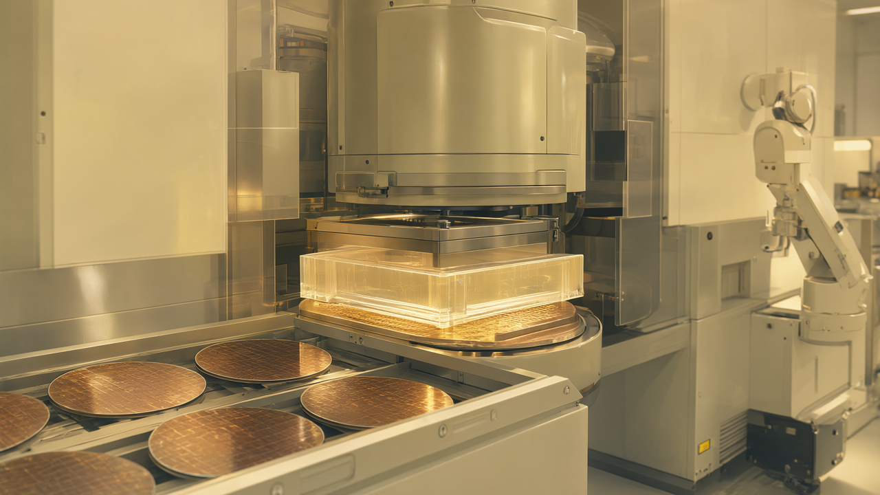
Canon has revealed its proactive engagement with customers to optimize mass production lines for its advanced nanoimprint lithography (NIL) systems. This initiative highlights the technology’s potential to drastically cut power consumption by approximately 90% during the critical exposure process in semiconductor manufacturing, thereby offering substantial improvements in sustainability and cost-efficiency for the miniaturizing semiconductor industry.
Technical / Clinical Details
Nanoimprint lithography operates by directly transferring patterns, leading to a simpler system architecture compared to complex optical lithography tools. This inherent simplicity is key to its dramatic energy savings, particularly in the exposure step. Through rigorous evaluation and optimization with customers, Canon is validating NIL systems’ capability to achieve an approximate 10-fold improvement in energy efficiency over conventional exposure technologies. This efficiency not only translates to reduced manufacturing costs but also significantly lowers the environmental footprint of the semiconductor industry. NIL technology is compatible with state-of-the-art 2nm process nodes, enabling the formation of high-density, uniform patterns with high fidelity.
Background & Context
The semiconductor manufacturing sector is experiencing ever-increasing demands for higher performance and greater miniaturization, which has simultaneously led to a critical challenge: escalating power consumption during manufacturing processes, especially lithography. Existing advanced exposure technologies like EUV, while high-performing, entail prohibitive capital expenditure, high operational costs, and immense power requirements. In this context, Canon’s NIL technology presents a clear advantage in low power consumption, positioning it as an attractive alternative for semiconductor manufacturers. The industry-wide push for sustainable manufacturing processes further elevates the significance and anticipation for NIL’s broader adoption.
Strategic Significance & Outlook
The progress in mass production line optimization achieved through Canon’s collaboration with its customers is expected to accelerate the widespread adoption of NIL technology. Moving forward, NIL is poised to enable the fabrication of energy-efficient semiconductors for a broad range of applications, including mobile devices, AI accelerators, and data centers. The maturation of this technology promises to drive down semiconductor manufacturing costs and reduce environmental impact, providing an essential foundation for the evolution of next-generation electronics.
Source: https://global.canon/en/technology/canon-tech/interview/nanoimprint/
Get our weekly technology intelligence — free
Receive an infographic that lets you judge at a glance whether each field’s analysis report is worth reading.
Subscribe Free — Weekly Tech Intelligence
By subscribing, you’ll receive Troy-Technical’s weekly technology intelligence newsletter.
- Your email and selected fields are used only to deliver the newsletter.
- We never share your information with third parties.
- You can unsubscribe anytime via the link in each email.
See our Privacy Policy for details.
Takes about a minute · Unsubscribe anytime