COMPANY PROFILE / AI & MACHINE LEARNING
TSMC
The manufacturing backbone of AI: it makes the chips and also performs the "connecting" steps such as CoWoS
Most GPUs and custom AI chips used to train and run AI are designed by one company and made by another. TSMC is the foundry that manufactures customers' designs, and HPC (high performance computing, which includes AI accelerators) was 58% of its 2025 revenue. This profile concentrates on leading-edge process technology and on advanced packaging such as CoWoS, which joins several chips and HBM into one package, within what the company has filed, published in its annual report and said on earnings calls. No CoWoS capacity figure appears in the company's official materials. We do not use press or research-firm numbers and say "not confirmed" instead. Products and investments change quickly, so every status carries its check date (15 October 2026).
- TSMC in 30 seconds, and where it stands in AI and machine learning
- The logo and how the name is written
- Where the company sits in the AI and machine learning field
- Scale (limited to the AI-related business)
- Resources committed to AI and machine learning
- What it has done so far
- What comes next
- What the company is aiming for in AI and machine learning
- Map of partnerships in AI and machine learning
- Technology, products and services
- The risks this company carries
- Glossary / References / Claim-to-source audit
1. TSMC in 30 seconds, and where it stands in AI and machine learning
NYSE: TSMTaiwan since September 1994; NYSE (ADSs) since October 1997
(contract manufacturing)It does not design chips for sale; it manufactures customers' designs. The classification is ours
(3DFabric)Capacity and standalone revenue are not disclosed
Before an AI chip reaches a customer there are two stages: making the wafer and packaging the chips and memory together. In its 20-F, TSMC says that besides leading-edge process technology it offers CoWoS (which puts several SoC chips and HBM stacks into one package) and SoIC (which stacks chips in three dimensions) as "3DFabric" Sourced. AI supply therefore depends not only on TSMC's wafer capacity but on its packaging capacity. The company, however, discloses neither its CoWoS capacity nor the revenue of advanced packaging on its own. The other feature is that sales are concentrated: in 2025 the ten largest customers were 78% of revenue, and the 20-F does not name them Sourced. This profile reads the company through those two points: a supply structure that includes packaging, and customer concentration.
2. The logo and how the name is written
A note on names: the legal entity is Taiwan Semiconductor Manufacturing Company Limited, shortened to TSMC. JASM (the Kumamoto fab) and ESMC (the Dresden fab) are separate companies in which TSMC holds a majority. VIS (Vanguard International Semiconductor) and GUC (Global Unichip) are separate listed companies in which TSMC holds stakes; they are not TSMC itself.
Official site: https://www.tsmc.com/english3. Where the company sits in the AI and machine learning field
4. Scale (limited to the AI-related business)
Most of TSMC's revenue is leading-edge logic wafers. The table shows company-wide figures, centred on the indicators closest to AI (HPC and advanced process). Figures are from the 20-F, in NT$ millions Sourced.
| Indicator (NT$ millions) | 2023 | 2024 | 2025 |
|---|---|---|---|
| Net revenue | 2,161,736 | 2,894,308 | 3,809,054 |
| of which HPC | 934,769 | 1,476,891 | 2,192,931 |
| HPC share | 43% | 51% | 58% |
| Gross margin | 54.4% | 56.1% | 59.9% |
| Advanced technologies (7nm and below), share of wafer revenue | 58% | 69% | 74% |
| R&D expense | 182,370 | 204,182 | 246,427 |
| Capital expenditure | 949,817 | 956,007 | 1,272,411 |
| Employees (year-end) | 76,478 | 83,825 | 90,557 |
Net income attributable to the parent in 2025 was NT$1,697,604 million, R&D was 6.5% of revenue, and wafer shipments were about 15.02 million 12-inch equivalents (about 12.91 million the year before). The 20-F says annual capacity exceeded 17 million 12-inch equivalent wafers Sourced. Wafer fabrication was about 86% of revenue; the remaining roughly 14% (our calculation) was mainly packaging and testing, mask making, design and royalties Our calculation.
Figures for the latest quarter (April to June 2026) are below. Check date: 15 October 2026 Sourced.
| Second quarter of 2026 | Value | Note |
|---|---|---|
| Net revenue | NT$1,270.38 billion (US$40.20 billion) | Up 36.0% year on year in NT dollars; up 33.7% in U.S. dollars |
| Gross margin | 67.7% | Share of revenue. 66.2% in the previous quarter |
| By platform | HPC 66% / smartphone 22% / IoT 5% / automotive 4% / consumer electronics 1% | As described on the earnings call |
| By technology (wafer revenue) | 2nm 3% / 3nm 30% / 5nm 33% / 7nm 11% (77% at 7nm and below) | Earnings release |
| Third-quarter outlook | Revenue US$44.6-45.8 billion; gross margin 65-67% | Company outlook; the steep 2nm ramp is said to dilute margin by 3-4 points Not yet confirmed |
| Full-year 2026 revenue | Growth slightly above 40% in U.S. dollars | Company outlook Not yet confirmed |
HPC is not the same as AI accelerators. The 20-F says HPC includes AI GPUs and AI ASICs but also PC CPUs, consumer GPUs, FPGAs, server processors and high-speed networking chips Sourced. The HPC share therefore cannot be read as the AI share of revenue. The revenue of AI accelerators on their own appears in neither the 20-F nor the earnings materials. On the July 2026 call, the head of investor relations recalled that in January 2026 the company had described AI growth over five years as "mid- to high-50s" percent a year, and the CEO said it is stronger than that but gave no number Not yet confirmed.
5. Resources committed to AI and machine learning
The table shows whether the four items (people, money, outside investments and joint ventures, and ties with universities and public bodies) could be confirmed in the 20-F, the annual report and the earnings call.
| Type of resource | Details | Status |
|---|---|---|
| People | 90,557 employees at the end of 2025 (83,825 a year earlier). The number dedicated to advanced packaging is not disclosed | Sourced |
| Money: R&D | NT$246,427 million in 2025 (US$7,855 million, 6.5% of revenue). R&D is split between centralized work (new logic and package technology) and fab-led work | Sourced |
| Money: capex | NT$1,272,411 million in 2025 (US$40,895 million). For 2026, US$52-56 billion in the 20-F, raised to US$60-64 billion on the July call. Allocation: 70-80% advanced process, about 10% specialty, 10-20% advanced packaging, testing, mask making and other (no standalone figure for packaging) | Sourced (2026 figures: Not yet confirmed) |
| Outside investments and JVs | JASM (Kumamoto) 72.6%, ESMC (Dresden) 70%, VIS 27.6%, SSMC 38.8%, GUC 34.8%, VisEra 67.2%, Xintec 41.0% (as of 28 February 2026). On 15 May 2026 announced the sale of an 8.1% stake in VIS (the second-quarter materials list it as sold). On 11 August 2026 announced an agreement with Sony Semiconductor Solutions to set up a joint venture for next-generation image sensors (this article confirmed only the announcement title) | Sourced |
| Public funding | U.S.: TSMC Arizona signed agreements with the Department of Commerce in November 2024 for up to US$6.6 billion in direct funding and up to US$5 billion in loans, subject to conditions and milestones. Germany: ESMC agreed in December 2024 to up to EUR 5 billion in state aid (European Chips Act). The 20-F notes that receipt depends on conditions | Sourced |
| Universities and research bodies | The 20-F mentions collaboration "with customers, equipment vendors and external research and development consortia" but names no specific university or institution that we could confirm. On standards, it says TSMC contributed the 3Dblox standard to the IEEE | Not confirmed |
| Advanced packaging facilities | Operates seven advanced backend fabs (20-F). Says it is building 13 leading-edge and advanced packaging fabs in Taiwan over the next several years and will invest a further US$100 billion in Arizona that includes advanced packaging fabs (company statements, July 2026) | Sourced (plans: Not yet confirmed) |
Key products and facilities, as far as the company's materials let us confirm (check date 15 October 2026). The generation and reticle labels are the company's own.
| Product or facility | Scale and content | Stage | Date | Source |
|---|---|---|---|---|
| 2nm (N2, nanosheet) | First nanosheet transistor generation; 3% of wafer revenue in the second quarter of 2026 | In volume production | 2025 (20-F) | Reference 1, 3 https://www.sec.gov/Archives/edgar/data/1046179/000162828026025362/tsm-20251231.htm https://www.sec.gov/Archives/edgar/data/1046179/000104617926000451/a2q26e_withguidancexfinal.htm |
| A16 | The generation after 2nm | Risk production expected in 2026 | Per the 20-F | Reference 1 https://www.sec.gov/Archives/edgar/data/1046179/000162828026025362/tsm-20251231.htm |
| A14 | Second-generation nanosheet | Risk production in 2027, volume production scheduled for 2028 Not yet confirmed | July 2026 | Reference 5 https://investor.tsmc.com/english/encrypt/files/encrypt_file/reports/2026-08/3e494f0c14dd0890f897aa044415e21d93486cc4/TSMC%202Q26%20Transcript.pdf |
| CoWoS-L (3.5-reticle) | RDL interposer plus local silicon interconnect (LSI) | In volume production since 2024 | Annual report | Reference 2 https://investor.tsmc.com/static/annualReports/2025/english/pdf/2025_tsmc_ar_e_ch5.pdf |
| CoWoS-L (5.5-reticle) | The annual report says in one place that certification was completed in 2025 with volume production starting in 2026, and in another that qualification finishes in 2026. The April 2026 release says it is "now producing" it | Production (wording differs by document) | April 2026 | Reference 2, 6 https://investor.tsmc.com/static/annualReports/2025/english/pdf/2025_tsmc_ar_e_ch5.pdf https://pr.tsmc.com/english/news/3302 |
| CoWoS-L (9.5-reticle) | Described as making good progress | In development Not yet confirmed | Annual report | Reference 2 https://investor.tsmc.com/static/annualReports/2025/english/pdf/2025_tsmc_ar_e_ch5.pdf |
| CoWoS (14-reticle and beyond) | The 14-reticle version is said to integrate about 10 large compute dies and 20 HBM stacks, in production in 2028, then beyond 14 reticles in 2029 | Plan Not yet confirmed | April 2026 | Reference 6 https://pr.tsmc.com/english/news/3302 |
| SoIC (3nm) / A14-to-A14 SoIC | The 3nm SoIC entered volume production in 2025. A14-to-A14 SoIC is slated for 2029, with 1.8X the die-to-die I/O density of N2-on-N2 | In production / plan Not yet confirmed | 2025; April 2026 | Reference 2, 6 https://investor.tsmc.com/static/annualReports/2025/english/pdf/2025_tsmc_ar_e_ch5.pdf https://pr.tsmc.com/english/news/3302 |
| COUPE (optical engine) | COUPE on substrate begins production in 2026; the company claims 2X power efficiency and 10X lower latency versus a pluggable on the circuit board | Production planned Not yet confirmed | April 2026 | Reference 6 https://pr.tsmc.com/english/news/3302 |
| SoW-X (wafer-scale) | A System-on-Wafer of 40-reticle size | Expected in 2029 Not yet confirmed | April 2026 | Reference 6 https://pr.tsmc.com/english/news/3302 |
| Arizona (Fab 21) | The first facility reached volume production at the end of 2024; the second is under construction; the third started in 2025; more land was acquired in 2026 | Operating / under construction | April 2026 (20-F) | Reference 1 https://www.sec.gov/Archives/edgar/data/1046179/000162828026025362/tsm-20251231.htm |
"Plan", "scheduled" and "expected" do not mean the outcome is certain. The reticle multiple is the package size relative to the largest area one exposure can print.
6. What it has done so far
| When | What happened | Why it matters |
|---|---|---|
| 1987 / 1994 / 1997 | Founded as a joint venture including the Taiwanese government; listed in Taiwan (1994) and on the NYSE as ADSs (1997) | A dedicated foundry from the start (20-F history) |
| March 2020 | With Broadcom, announced a CoWoS 2X-reticle interposer (about 1,700 mm²) able to hold up to six HBM stacks | An early step on the path of larger interposers and more HBM stacks |
| From 2023 | The annual report says CoWoS has been "experiencing strong growth due to surging AI demand since 2023" | The company attributes the rise in advanced-packaging demand to AI |
| 2024 | 3.5-reticle CoWoS-L entered production. In April, an MOU with SK hynix on the HBM4 base die and CoWoS integration. In November, the CHIPS Act agreements with the U.S. Department of Commerce; in December, the German state-aid agreement for ESMC. Arizona and Kumamoto reached volume production by year-end | A year in which both packaging and overseas sites expanded |
| 2025 | 2nm entered volume production; the 3nm SoIC entered volume production; certification of 5.5-reticle CoWoS-L completed. In December, the U.S. Section 232 proclamation on semiconductor imports | Next generations on both process and packaging, alongside changes in trade policy |
| April 2026 | Filed the 20-F (16 April). At its technology symposium, presented A13 and plans for 14-reticle CoWoS, SoW-X and COUPE (22-23 April) | Set out the product path toward 2028-2029 |
| July 2026 | On the earnings call, raised the capital budget to US$60-64 billion and described an additional US$100 billion in Arizona and the construction of 13 fabs in Taiwan | The scale of investment rose sharply within a year |
| August-September 2026 | Agreed with Sony Semiconductor Solutions to set up an image sensor joint venture (11 August). With ASML, announced an initiative on 12-inch photomasks for High NA EUV (8 September) | Partnerships are widening around manufacturing |
7. What comes next
The company presents these as outlook and plans, not as achieved facts Not yet confirmed. On equipment supply, it says it coordinates with tool suppliers well in advance and does not foresee bottlenecks to its expansion plans.
None of the following could be confirmed in the company's 20-F, annual report, earnings materials or call transcript Not yet confirmed: CoWoS monthly capacity and expansion figures; standalone revenue and capex for advanced packaging (the company groups "packaging, testing, mask making and other" together at 10-20%); customer names and revenue by customer; the absolute value of AI accelerator revenue; monthly wafer output by product. Capacity figures and customer allocations given by the press or research firms are not official company materials and are not used here.
8. What the company is aiming for in AI and machine learning
This chapter includes points the company does not state directly. They are written as inferences from primary sources, with the evidence alongside.
| What can be read | Primary evidence | Status |
|---|---|---|
| It sees supply limits spreading beyond wafers into packaging and testing and shifts equipment spending accordingly | 10-20% of the capital budget goes to advanced packaging, testing, mask making and other. The CEO said that, depending on customers' products, testers run short and spending shifts between front end and back end | Inference |
| It aims for integrated supply that includes packaging in Arizona | The added US$100 billion is described as for logic fabs and advanced packaging fabs | Inference |
| It keeps several options for "what comes after CoWoS" | CoWoS beyond 14 reticles, SoW-X, COUPE on substrate and alternatives such as glass substrates (the CEO said the majority is still CoWoS and that the alternative pipeline needs about another year) | Inference |
| Overseas expansion proceeds with the margin dilution built in | Overseas ramp-ups are expected to dilute gross margin by 2-3 points at first and 3-4 points later | Sourced |
| The company itself expects concentration in a few customers to continue | The 20-F says system companies increasingly design their own semiconductors and work directly with foundries. The ten largest customers were 78% of revenue | Sourced |
On the July 2026 call an analyst asked for the capex split for advanced packaging alone. The company answered with a combined band of "advanced packaging, testing, mask making and other" at 10-20%, and the CEO said it cannot split this finely because it moves money to wherever a bottleneck appears, front end or back end Sourced. The same answer said that, depending on customers' products, testers are in short supply. From this we read that AI chip supply depends not only on wafer capacity but on back-end equipment (packaging and testing), and that the company steers its spending on that premise. Because the back-end amount itself is undisclosed, its scale cannot be judged Not yet confirmed.
9. Map of partnerships in AI and machine learning
10. Technology, products and services
| Layer | Main technologies | What the 20-F and annual report say |
|---|---|---|
| Leading-edge logic | N2 (2nm nanosheet), N3, N4, N5, A16, and the HPC-focused N4X, N3X and N2X | Offers leading-edge logic and high-speed interconnect IP for HPC; N4X, N3X and N2X target the maximum performance and clock speed in each family |
| 3D stacking | TSMC-SoIC (chip-on-wafer) | Provides high-density interconnect for chiplet-based HPC; the 3nm SoIC entered volume production in 2025 |
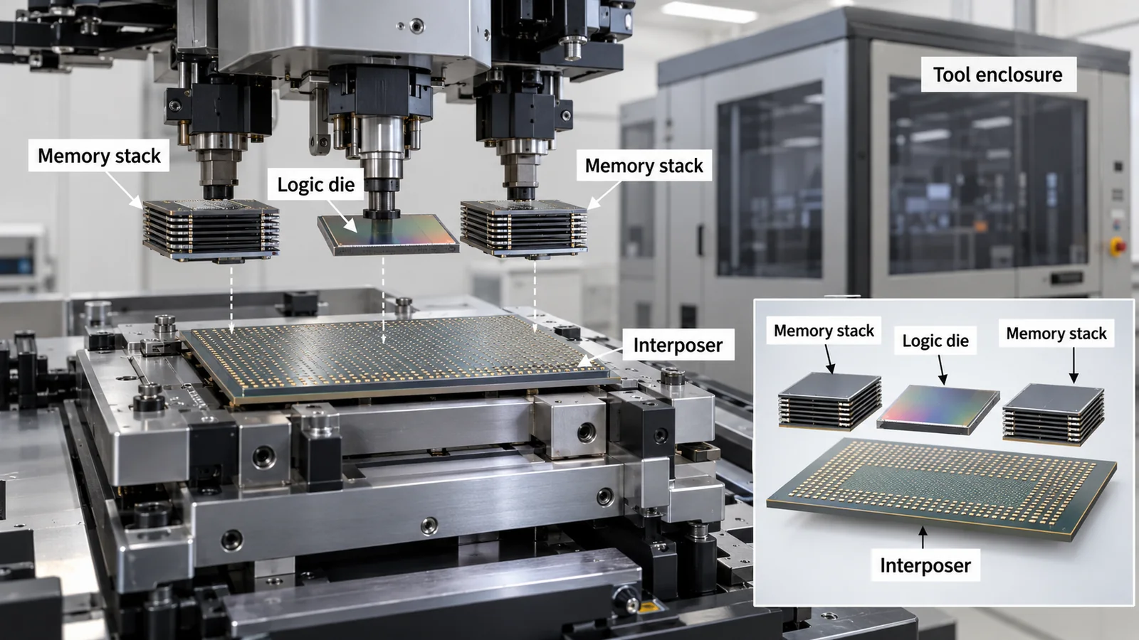
| 2.5D packaging | CoWoS-S / CoWoS-R / CoWoS-L | Joins SoC chips and HBM stacks to raise compute and memory bandwidth. S = silicon interposer, R = RDL interposer, L = RDL plus local silicon interconnect |
| Wafer scale | TSMC-SoW / SoW-X | Wafer-level heterogeneous integration for data center compute chips; the first generation is logic only |
| Optical connection | COUPE and CoWoS CPO | Combines silicon photonics and control chips. COUPE is expected in volume production in 2026; CPO is a method under development that puts an interposer-based module and COUPE into one package |
| Design infrastructure | 3Dblox, 3DIC reference flows and the Open Innovation Platform | TSMC contributed the 3Dblox standard to the IEEE; the annual report also mentions design support aligned with the IEEE P3537 standard |
Memory bandwidth and the interposer: the annual report describes CoWoS as bringing SoC chips and HBM stacks close together in one package to raise compute and memory bandwidth Sourced. The S type has high routing density and embedded capacitors (eDTC); the L type adds local silicon interconnect (LSI) in an RDL interposer to support larger sizes. To carry several compute dies and HBM stacks, larger interposers (the reticle multiple) are the axis of progress (our reading; see our explainers on CoWoS, HBM and heterogeneous integration).
Substrate and heat: in large packages, substrate warpage and heat removal become issues. Asked in July 2026 about newer approaches such as glass substrates, the CEO said the majority is still CoWoS and that the pipeline for alternatives needs about another year to mature. Intel's 10-K also refers to an industry-wide shortage of substrates (see our Intel profile).
Power and process: 2nm is the first nanosheet generation, and A12, previewed in April 2026, adds backside power delivery (Super Power Rail) as planned for 2029. Splitting routing between front and back to deliver power suggests an aim of handling the high currents of HPC Not yet confirmed.
Connecting with light: COUPE puts the optical engine inside the package, and the company says it gives 2X power efficiency and 10X lower latency than a pluggable on the circuit board. That is the company's stated value; the comparison conditions are not confirmed here (see our explainers on co-packaged optics and optical interconnects and SerDes).
Raw materials: the 20-F says the main raw materials are silicon wafers, chemicals, gases and precious metals; most wafers come from a limited number of suppliers in Taiwan, Japan, Germany and Singapore, and some materials are sole-sourced Sourced.
11. The risks this company carries
| Risk | Details | Status |
|---|---|---|
| Customer concentration | The ten largest customers were 78% of revenue (76% in 2024, 70% in 2023). The largest was 19% (22%, 25%) and the second 17% (12%, 11%). Names are not disclosed | Sourced |
| Export controls | Under the January 2025 U.S. rules, shipping products made at 16nm or below to specified destinations may need a licence unless conditions are met. The Nanjing fab's VEU authorization expired in December 2025 and was replaced by an annual export licence (renewal is not assured). At the time of the 20-F, results had not been materially affected | Sourced |
| Tariffs and trade | A December 2025 U.S. proclamation imposes a 25% tariff on certain advanced computing chips meeting specified performance thresholds (excluding imports for designated U.S. use). In January 2026 the U.S. and Taiwan announced a trade and investment agreement; in February 2026 the U.S. Supreme Court ruled the IEEPA tariffs unlawful. The 20-F says the effects remain unclear | Sourced |
| An export-control notification | In October 2024 TSMC notified U.S. and Taiwan authorities that one type of customer chip it made might have been diverted to, or incorporated in the product of, a restricted entity, and it has cooperated with requests for further information. The 20-F gives no conclusion, and this article does not speculate | Sourced |
| Geographic concentration | Most principal executives and production facilities are in Taiwan, and most revenue derives from operations there. Earthquakes in April 2024 and January 2025 caused losses of about NT$3 billion and NT$5.3 billion (net of insurance) | Sourced |
| Capex and demand | The 2026 capital budget is US$60-64 billion. The 20-F warns that if demand does not materialise, the added cost could weigh on results. Dependence on AI demand is also large (HPC was 66% in the second quarter of 2026) | Sourced |
| Overseas margins and subsidy conditions | Overseas ramp-ups are expected to dilute gross margin by 2-3 points, later 3-4 points. The 20-F notes that subsidies may be reduced or repaid if conditions are breached | Sourced |
| Competition and antitrust | The 20-F points to competitors that may receive government subsidies, customers who may seek more suppliers, and heightened antitrust risk | Sourced |
12. Glossary
- Foundry
- A company that manufactures semiconductors designed by its customers. TSMC is a dedicated foundry that manufactures rather than designs and sells chips.
- HPC
- High performance computing. In TSMC's categories it includes AI accelerators, PC CPUs, FPGAs and more.
- CoWoS
- Chip on Wafer on Substrate. A 2.5D technology that places a compute chip and HBM side by side on an interposer in one package.
- SoIC
- System on Integrated Chips. TSMC's name for bonding chips directly and stacking them in three dimensions.
- 3DFabric
- TSMC's umbrella name for its 3D stacking and packaging technologies, including SoIC, CoWoS, InFO and SoW.
- HBM
- High bandwidth memory. Memory stacked right next to a compute chip.
- Reticle
- The largest area an exposure tool can print at once (about 26 x 33 mm). "5.5-reticle" means a package about 5.5 times that area.
- Interposer
- An intermediate wiring layer that connects chips to each other and to the substrate; it may be silicon or RDL (redistribution layer).
- COUPE
- Compact Universal Photonic Engine, TSMC's silicon photonics engine for optical signals.
- Nanosheet
- A newer transistor structure in which the gate surrounds thin sheets; adopted from TSMC's 2nm (N2).
- VEU
- Validated End-User: a U.S. export-control authorization allowing items to be supplied to a specific facility without individual licences.
- Form 20-F
- The annual report that foreign companies listed in the U.S. file with the SEC.
13. References
- TSMC Annual Report on Form 20-F for the fiscal year ended December 31, 2025 (filed with the U.S. SEC on 16 April 2026). Business, revenue by platform, customer concentration, capital expenditure, R&D, headcount, subsidiaries and holdings, export controls and tariffs, risk factors. https://www.sec.gov/Archives/edgar/data/1046179/000162828026025362/tsm-20251231.htm
- TSMC 2025 Annual Report, Chapter 5 "Business Activities". The status of 3DFabric (SoIC, CoWoS, SoW, COUPE) in production and development, and the CoWoS stages by reticle size. https://investor.tsmc.com/static/annualReports/2025/english/pdf/2025_tsmc_ar_e_ch5.pdf
- TSMC TSMC Reports Second Quarter EPS of NT$27.25 (earnings release, exhibit to Form 6-K, 16 July 2026). Second-quarter revenue, margins, revenue by technology and the third-quarter outlook. https://www.sec.gov/Archives/edgar/data/1046179/000104617926000451/a2q26e_withguidancexfinal.htm
- TSMC 2026 Second Quarter Earnings Conference Presentation Material (exhibit to Form 6-K, 16 July 2026). Financial statement extracts and the 2026 revenue outlook. https://www.sec.gov/Archives/edgar/data/1046179/000104617926000451/a2q26presentatione.htm
- TSMC Q2 2026 Taiwan Semiconductor Manufacturing Co Ltd Earnings Call (edited transcript by LSEG StreetEvents, 16 July 2026, hosted on TSMC's investor site). The capital budget and its allocation, the added Arizona investment, new fabs in Taiwan and the HPC share. https://investor.tsmc.com/english/encrypt/files/encrypt_file/reports/2026-08/3e494f0c14dd0890f897aa044415e21d93486cc4/TSMC%202Q26%20Transcript.pdf
- TSMC TSMC Debuts A13 Technology at 2026 North America Technology Symposium (press release, issued 23 April 2026). A13 and A12, and the plans for CoWoS, SoW-X, SoIC and COUPE. https://pr.tsmc.com/english/news/3302
- TSMC and ASML ASML and TSMC Announce Initiative to Pioneer Industry Transition to Large-Format Photomasks for High NA EUV (joint press release, 8 September 2026). https://pr.tsmc.com/english/news/3338
- TSMC and Broadcom TSMC and Broadcom Enhance the CoWoS Platform with World's First 2X Reticle Size Interposer (press release, 3 March 2020). https://pr.tsmc.com/english/news/2026
- SK hynix SK hynix Partners with TSMC to Strengthen HBM Technological Leadership (SK hynix press release, 19 April 2024, with a comment from a TSMC executive). Collaboration on HBM4 and CoWoS. https://news.skhynix.com/en/sk-hynix-partners-with-tsmc-to-strengthen-hbm-technological-leadership/
- TSMC Source of the logo image (an image inside TSMC's earnings release, filed with Form 6-K; checked 15 October 2026). https://www.sec.gov/Archives/edgar/data/1046179/000104617926000451/image_1.jpg

14. Claim-to-source audit
| Claim in the text | Status | Reference |
|---|---|---|
| Legal name, headquarters and listing history | Sourced | Reference 1 https://www.sec.gov/Archives/edgar/data/1046179/000162828026025362/tsm-20251231.htm |
| Revenue, HPC revenue, gross margin, R&D, capex and headcount, 2023-2025 | Sourced | Reference 1 https://www.sec.gov/Archives/edgar/data/1046179/000162828026025362/tsm-20251231.htm |
| Ten largest customers 78% of revenue; largest 19%, second 17% (2025) | Sourced | Reference 1 https://www.sec.gov/Archives/edgar/data/1046179/000162828026025362/tsm-20251231.htm |
| Wafer fabrication about 86% of revenue; the rest is packaging, testing and other | Sourced | Reference 1 https://www.sec.gov/Archives/edgar/data/1046179/000162828026025362/tsm-20251231.htm |
| Seven advanced backend fabs; 2nm volume production in 2025; A16 risk production expected in 2026 | Sourced | Reference 1 https://www.sec.gov/Archives/edgar/data/1046179/000162828026025362/tsm-20251231.htm |
| 2026 capex of US$52-56 billion (20-F) | Not yet confirmed | Reference 1 https://www.sec.gov/Archives/edgar/data/1046179/000162828026025362/tsm-20251231.htm |
| Subsidiaries and holdings (JASM 72.6%, ESMC 70%, VIS, GUC, SSMC and others) | Sourced | Reference 1 https://www.sec.gov/Archives/edgar/data/1046179/000162828026025362/tsm-20251231.htm |
| U.S. CHIPS Act funding (up to US$6.6 billion) and loans (up to US$5 billion); German state aid (up to EUR 5 billion) | Sourced | Reference 1 https://www.sec.gov/Archives/edgar/data/1046179/000162828026025362/tsm-20251231.htm |
| Export controls (the January 2025 rules, the end of the VEU for the Nanjing fab and its annual licence) and tariffs (Section 232 and others) | Sourced | Reference 1 https://www.sec.gov/Archives/edgar/data/1046179/000162828026025362/tsm-20251231.htm |
| The October 2024 notification to U.S. and Taiwan authorities (a customer chip may have reached a restricted entity) | Sourced | Reference 1 https://www.sec.gov/Archives/edgar/data/1046179/000162828026025362/tsm-20251231.htm |
| Earthquake losses in Taiwan (NT$3 billion in 2Q 2024, NT$5.3 billion in 1Q 2025) | Sourced | Reference 1 https://www.sec.gov/Archives/edgar/data/1046179/000162828026025362/tsm-20251231.htm |
| The production and development status of CoWoS, SoIC, SoW and COUPE; 3.5-reticle CoWoS-L in production since 2024, 5.5-reticle starting volume production in 2026, 9.5-reticle in development | Sourced | Reference 2 https://investor.tsmc.com/static/annualReports/2025/english/pdf/2025_tsmc_ar_e_ch5.pdf |
| Second-quarter 2026 revenue, gross margin and revenue by technology; the third-quarter outlook | Sourced | Reference 3 https://www.sec.gov/Archives/edgar/data/1046179/000104617926000451/a2q26e_withguidancexfinal.htm |
| Expects 2026 revenue to grow slightly above 40% in U.S. dollar terms | Not yet confirmed | Reference 4 https://www.sec.gov/Archives/edgar/data/1046179/000104617926000451/a2q26presentatione.htm Reference 5 https://investor.tsmc.com/english/encrypt/files/encrypt_file/reports/2026-08/3e494f0c14dd0890f897aa044415e21d93486cc4/TSMC%202Q26%20Transcript.pdf |
| Raised the 2026 capital budget to US$60-64 billion; allocation 70-80% advanced process, about 10% specialty, 10-20% advanced packaging and other | Not yet confirmed | Reference 5 https://investor.tsmc.com/english/encrypt/files/encrypt_file/reports/2026-08/3e494f0c14dd0890f897aa044415e21d93486cc4/TSMC%202Q26%20Transcript.pdf |
| HPC at 66% of second-quarter 2026 revenue; the margin effect of overseas fabs (2-3%, later 3-4%) | Sourced | Reference 5 https://investor.tsmc.com/english/encrypt/files/encrypt_file/reports/2026-08/3e494f0c14dd0890f897aa044415e21d93486cc4/TSMC%202Q26%20Transcript.pdf |
| An additional US$100 billion in Arizona and 13 leading-edge and advanced packaging fabs in Taiwan (company plans) | Not yet confirmed | Reference 5 https://investor.tsmc.com/english/encrypt/files/encrypt_file/reports/2026-08/3e494f0c14dd0890f897aa044415e21d93486cc4/TSMC%202Q26%20Transcript.pdf |
| The CEO's remarks on advanced packaging capital spending (tester shortage, flexibility between front and back end) | Sourced | Reference 5 https://investor.tsmc.com/english/encrypt/files/encrypt_file/reports/2026-08/3e494f0c14dd0890f897aa044415e21d93486cc4/TSMC%202Q26%20Transcript.pdf |
| Now producing 5.5-reticle CoWoS; 14-reticle in 2028, beyond 14 in 2029, SoW-X in 2029, COUPE on substrate in 2026; timing of A13, A12 and N2U | Not yet confirmed | Reference 6 https://pr.tsmc.com/english/news/3302 |
| The joint initiative with ASML on 12-inch photomasks (pilot line by 2031, advanced-node production by 2033 as the aim) | Not yet confirmed | Reference 7 https://pr.tsmc.com/english/news/3338 |
| The 2020 CoWoS 2X-reticle interposer with Broadcom (about 1,700 mm², up to six HBM stacks) | Sourced | Reference 8 https://pr.tsmc.com/english/news/2026 |
| The April 2024 MOU with SK hynix (TSMC logic process for the HBM4 base die; optimising HBM-CoWoS integration) | Sourced | Reference 9 https://news.skhynix.com/en/sk-hynix-partners-with-tsmc-to-strengthen-hbm-technological-leadership/ |
| Source of the logo image | Sourced | Reference 10 https://www.sec.gov/Archives/edgar/data/1046179/000104617926000451/image_1.jpg |
| The four-type classification and where TSMC sits | Our calculation | Our own classification; company names are examples from firms covered in this series (this article) |
| The roughly 14% of revenue outside wafer fabrication | Our calculation | Our calculation (100% minus 86%) |
| CoWoS monthly capacity; standalone advanced-packaging revenue and capex; customer names; the absolute value of AI accelerator revenue | Not yet confirmed | No figures in the 20-F, the annual report or the earnings materials; press and research-firm figures are not used. These are items we could not confirm, not company outlook |
| The readings that the company is widening its supply limits into packaging and testing, aims at integrated production in Arizona, and keeps several "next after CoWoS" options | Inference | This article's interpretation of the 20-F, the earnings call and the press releases |
| The materials engineer's view (interposer, memory bandwidth, substrate, heat, power, optics) | Commentary | General technical commentary, not a company disclosure |
Last updated 15 October 2026 / Troy Technical
Figures in this article come from TSMC's statutory filings with the U.S. Securities and Exchange Commission (Form 20-F and Form 6-K), its annual report, its earnings call transcript and its press releases. No research-firm estimates or press-based figures have been used. Facility and product plans are company outlook, not achieved facts. Passages marked "Inference" are this article's interpretation of primary sources, not statements made by the company.