SEMICONDUCTOR FABRICATION · INTRODUCTION 1-1
What Is a Semiconductor?
How a carefully engineered crystal turns light into pictures, voltages into decisions, and electricity into useful work.
- Start with the photograph on your phone
- More useful than “halfway between a conductor and an insulator”
- Why the crystal matters
- The band gap: an energy rule, not a tiny space
- How can a missing electron carry current?
- Doping: a tiny change with a large effect
- A p–n junction makes movement directional
- From a junction to a solar panel, a camera and an LED
- The transistor: use one voltage to control another current
- From one transistor to an integrated circuit
- What fabrication has to achieve
- Check your understanding
- A short glossary
- Sources and further reading
Begin with the main text. The shaded physics boxes add optional detail and worked estimates. Figures are conceptual and not to scale. Numbered links lead to the supporting sources.
By the end, you should be able to describe what makes a semiconductor controllable, distinguish a band gap from a physical gap, explain how electrons and holes carry current, and connect a p–n junction and a transistor to familiar devices. No prior knowledge of quantum physics is needed. The optional calculation boxes take the ideas a little further.
Start with the photograph on your phone
Point a mobile phone at a friend, tap the shutter and look at the photograph. Several quite different jobs have just happened inside devices made from semiconductors. The camera converted incoming light into electrical signals. Processing circuits transformed those signals into a picture. Memory stored the result. The display produced or controlled light so that you could see it. Meanwhile, power circuits delivered the voltages each part needed.
It is tempting to imagine a semiconductor as a special substance with a single remarkable property. A more useful starting point is this: we can engineer where charge is available and how easily it moves. With different materials, structures and connections, that control becomes a light detector, a switch, a memory cell or a light source.
| Familiar action | What the device does | The semiconductor connection |
|---|---|---|
| Taking a photograph | Measures the light falling on many tiny regions | Absorbed photons create electrical charge that can be collected |
| Opening an app | Changes and combines electrical logic states | Transistors control conducting paths |
| Lighting an LED torch | Converts electrical energy into light | Electrons and holes recombine in a light-emitting structure |
| Charging a battery | Converts and regulates electrical power | Power transistors switch current through a conversion circuit |
These jobs do not all use the same semiconductor. Silicon dominates computing, but an efficient blue LED uses a different family of materials. The material sets the possibilities; the device structure makes a particular job possible.
A semiconductor material is a substance such as silicon. A semiconductor device is an engineered structure made using that material, such as a diode or transistor. An integrated circuit, or chip, combines many devices and their connections. The words are often used loosely in everyday conversation, but keeping them separate makes the physics much easier to follow.
More useful than “halfway between a conductor and an insulator”
Copper carries current readily. Glass usually does not. Semiconductors are often introduced as materials whose conductivity lies somewhere between the two. That description is a starting point, but it misses the reason they are useful.
A copper wire is valuable because it conducts reliably. A transistor is valuable because its ability to conduct can be changed. In a semiconductor, small amounts of selected impurities, an electric field, light and temperature can strongly alter the number of mobile charge carriers or their movement. We exploit those responses deliberately.
Silicon does not become a useful chip simply by being less conductive than copper. It becomes useful when we can create neighbouring regions with different electrical behaviour, put an insulating layer precisely where it is needed, and use a voltage to control a conducting path.
At about room temperature, intrinsic silicon has a resistivity of roughly 320,000 Ω·cm, whereas annealed copper at 20 °C is about 0.000001724 Ω·cm. Dividing the two gives approximately 190 billion. These are representative bulk values at slightly different reference temperatures, not a specification for every sample. Impurities, temperature and crystal quality matter. [1][2]
The point is the enormous range available to engineering. Silicon containing an appropriate concentration of dopants can be vastly more conductive than intrinsic silicon, while an insulating oxide can sit directly above it in the same device.
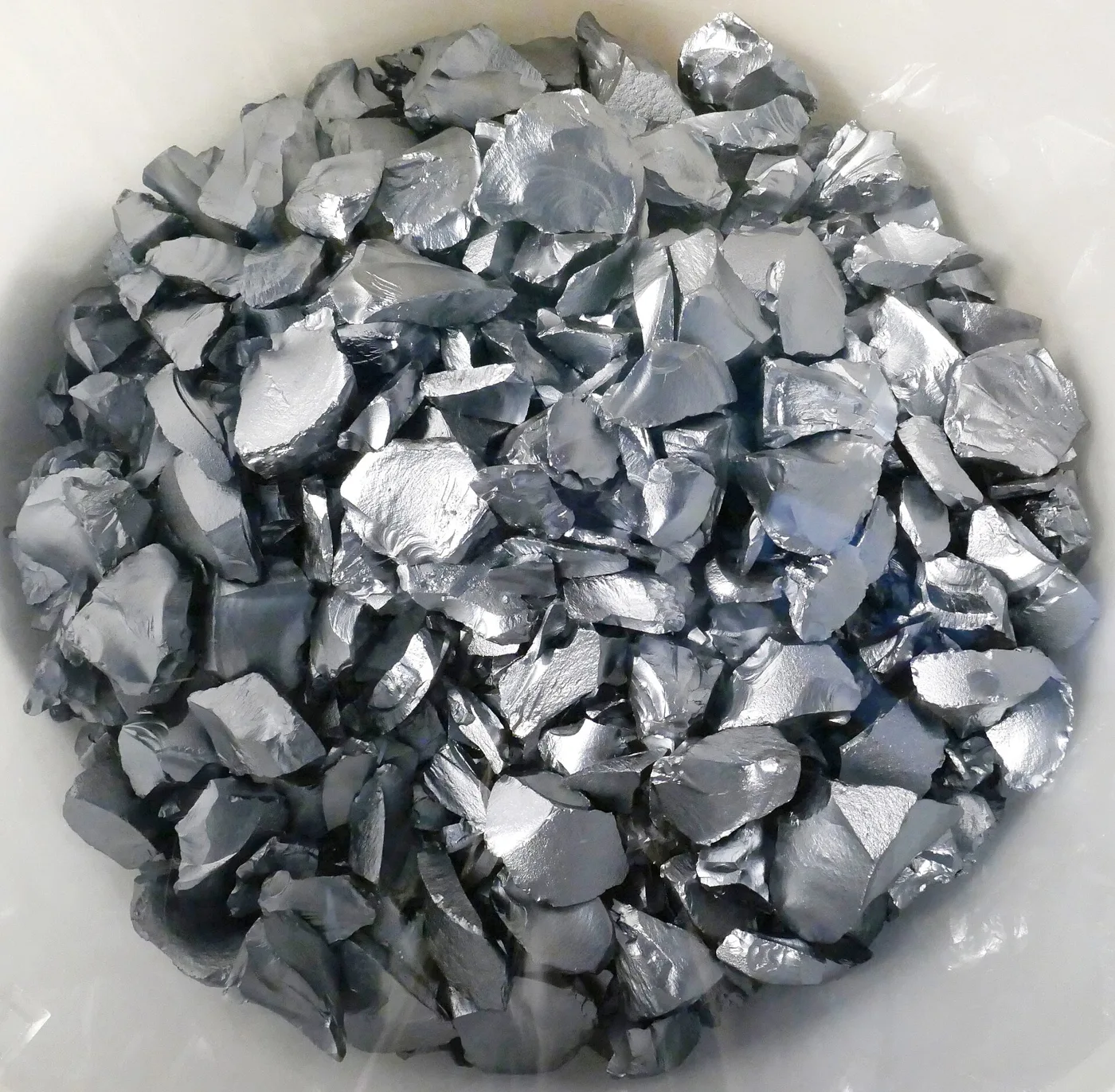
Why the crystal matters
A silicon atom has four electrons in its outer shell. In the crystal, each atom forms bonds with four neighbours. Electrons are shared in these covalent bonds. The local arrangement is three-dimensional: the four neighbours lie in tetrahedral directions around the central atom.
You can think of the crystal as an exceptionally orderly framework. That order allows us to predict how electrons behave throughout the material. It also explains why unwanted atoms, missing atoms and other defects can change device behaviour. Some impurities are introduced on purpose; others must be kept under extremely tight control.
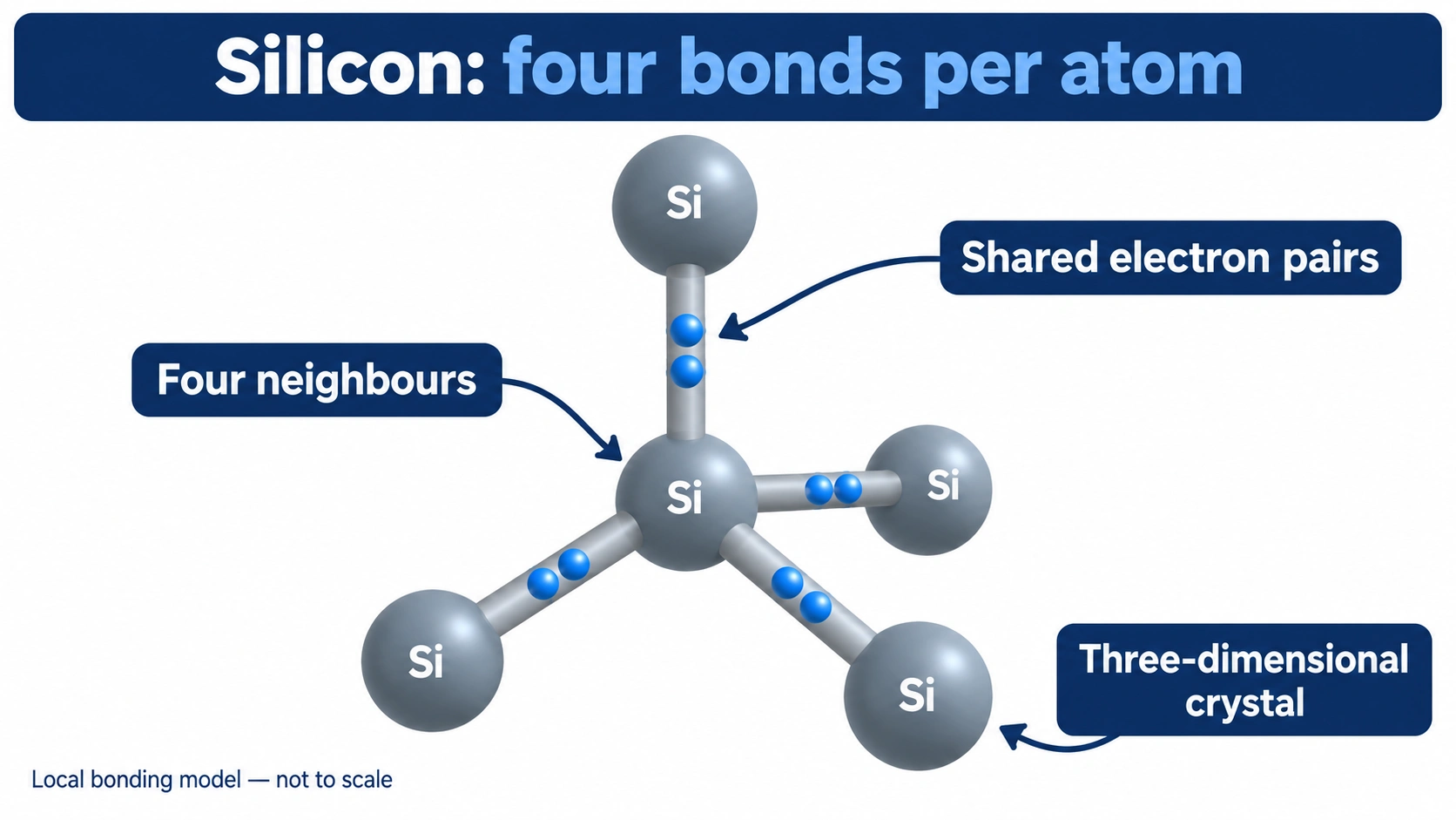
A drawing with neat sticks between atoms is a model, not a photograph of tiny rods. Electrons in a solid are described by quantum states extending through the material. The bond picture helps explain the local structure; the band picture in the next section explains which electronic states are available.
Silicon's cubic lattice constant is about 0.543 nm. This describes the repeating unit cell, not the distance along one individual silicon–silicon bond. A nanometre is one billionth of a metre. [3]
Silicon combines useful electronic properties with a particularly valuable oxide, silicon dioxide. That oxide can provide insulation and a well-controlled interface in transistor structures. Decades of manufacturing development have also made extremely pure crystals and extraordinarily precise processing possible. Abundance helps, but abundance alone does not explain silicon's success.
The band gap: an energy rule, not a tiny space
An electron in a solid cannot have just any energy. There are ranges of allowed electronic states, called bands, separated by ranges in which the crystal has no allowed bulk electronic states. The relevant forbidden range is the band gap.
The two bands we need first are the valence band and the conduction band. In a simple picture of silicon at very low temperature, the valence band is full and the conduction band is empty. A completely full band cannot produce a net electrical current in response to a small applied field: the occupied states balance one another. That does not mean its electrons are motionless.
Give an electron enough energy and it can be excited into the conduction band. The missing electron left in the valence band is called a hole. There are now two mobile carriers to discuss: a conduction-band electron and a valence-band hole.
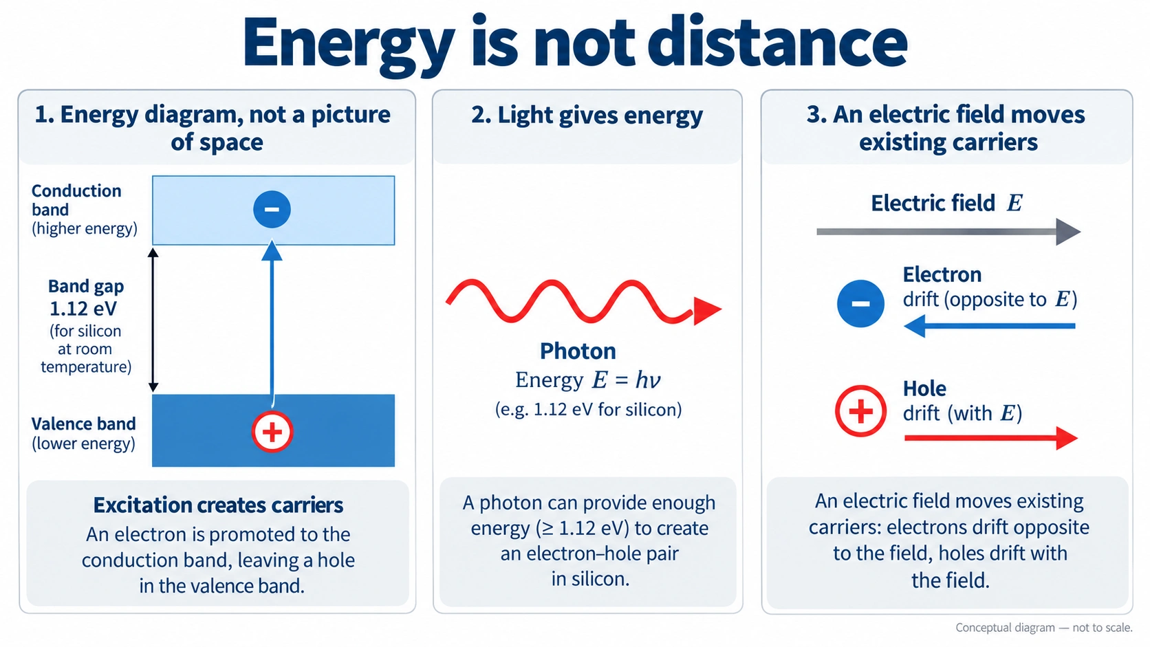
For silicon near room temperature, the band gap is about 1.12 electronvolts, usually written 1.12 eV. An electronvolt is a small unit of energy. The gap is not a distance between atoms, the thickness of an insulating film, or a threshold voltage that every circuit must exceed. [1]
This distinction prevents a common misunderstanding. An electron does not have to jump across the full band gap every time it moves along a wire or a transistor channel. Once mobile carriers exist, an electric field can change their average motion within the states available to them. Creating a carrier and transporting a carrier are different processes.
What light contributes
Light arrives in packets of energy called photons. A photon's energy depends on its wavelength: shorter wavelengths carry more energy per photon. A useful approximation is:
Photon energy in eV ≈ 1240 ÷ wavelength in nm.
A 620 nm photon carries about 2.0 eV, enough for band-to-band excitation in silicon if it is absorbed. A 1550 nm photon carries only about 0.80 eV, below silicon's band gap. Ordinary silicon photodetection therefore becomes ineffective beyond a wavelength of roughly 1100 nm. Real detector response also depends on absorption depth, reflection, thickness and device design. [4]
Turning up the brightness increases the number of photons arriving; it does not increase the energy of each photon at a fixed wavelength. Under ordinary operating conditions, many below-gap photons do not simply combine into one above-gap photon. Special high-intensity and defect-assisted processes are outside this introductory model.
What temperature contributes
Even in very pure silicon, thermal energy produces some electrons and holes at room temperature. These are continually generated and continually recombine. At equilibrium, the average concentrations settle to temperature-dependent values.
The intrinsic carrier concentration of silicon is roughly 1010 per cubic centimetre near 300 K, about 27 °C. That sounds large until you compare it with about 5 × 10²² silicon atoms in the same volume: roughly one conduction electron for every five trillion atoms. Values depend on the model and reference used. [1]
A common approximate relationship is ni ∝ T3/2 exp[−Eg/(2kT)]. It describes an equilibrium carrier concentration, not the probability that one particular electron jumps the gap.
If we hold silicon's band gap at 1.12 eV for a simplified calculation, increasing temperature from 300 K to 350 K raises this concentration by about 28 times; at 400 K it is about 350 times the 300 K value. The real band gap also changes with temperature. The practical lesson is that temperature can strongly affect leakage and sensor noise, even when a device is doing no useful work. [1][5]
How can a missing electron carry current?
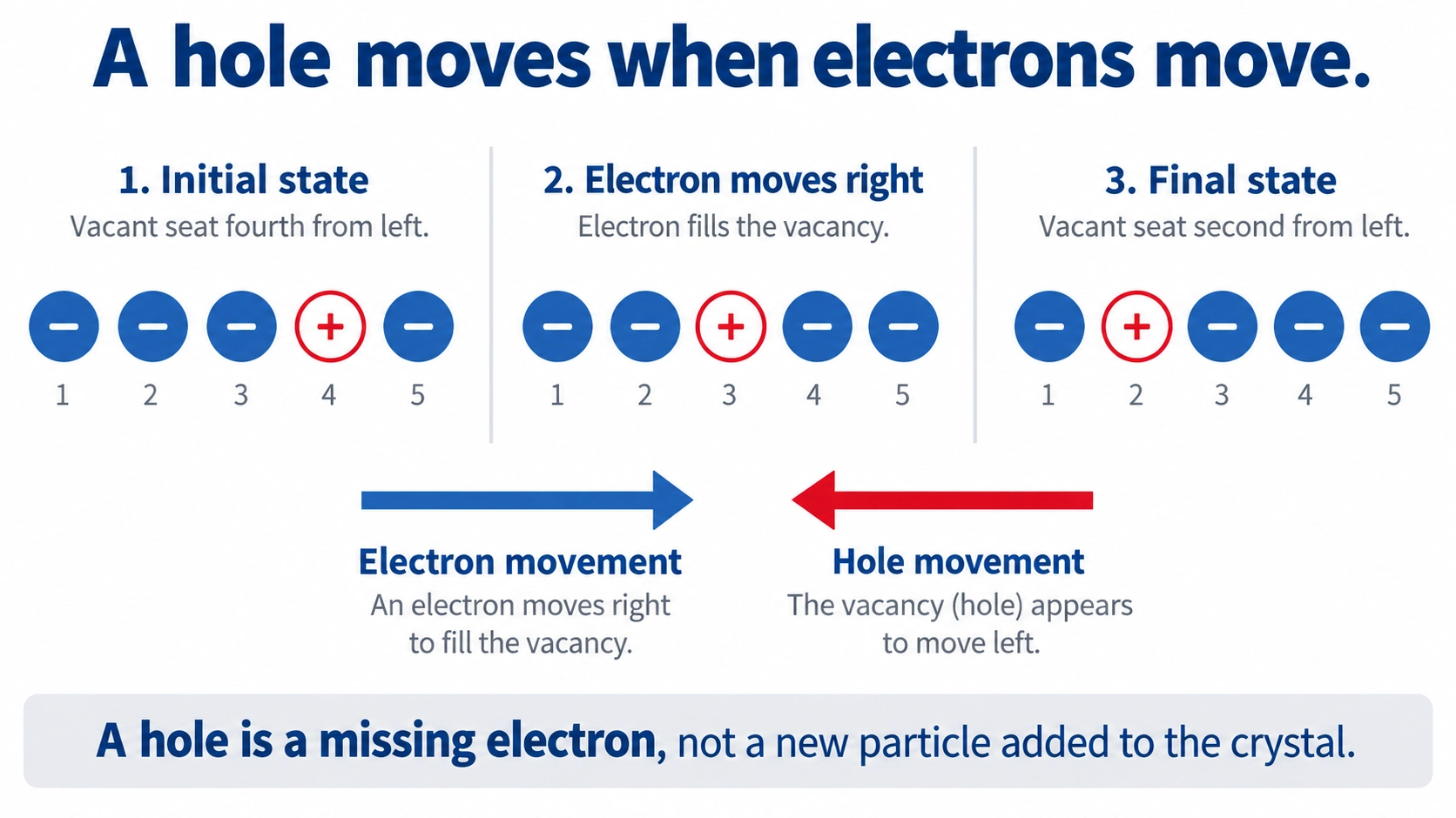
Imagine a row of occupied seats with one empty place. A person steps into the empty seat. Another person steps into the new vacancy. Everyone who moves goes one way, while the empty place appears to travel the other way.
In a valence band, neighbouring electrons can fill an unoccupied state. Tracking the vacancy is often much simpler than tracking all the electrons involved. We call that vacancy a hole and describe it as a mobile positive charge carrier. It is not a proton travelling through the crystal, and it is not an extra particle that we have inserted into the lattice.
Random movement, drift and diffusion
Carriers move and scatter even when there is no net current. Apply an electric field and a small average motion is added to this random activity. This is drift. Electrons drift opposite to the field because their charge is negative. Holes drift in the direction of the field because their effective charge is positive.
There is another route to current: diffusion. If carriers are crowded into one region, their random motion tends to spread them into less crowded regions. A concentration gradient can therefore produce a net carrier flow even without an applied electric field.
| Mechanism | What drives it? | A practical example |
|---|---|---|
| Drift | An electric field | A field helps separate light-generated carriers in a photodiode |
| Diffusion | A difference in carrier concentration | Injected carriers spread away from a junction |
| Recombination | An electron fills a hole through an allowed process | Charge is lost before collection, or light is emitted in a suitable LED |
Both drift and diffusion are essential to understanding a p–n junction. Thinking only in terms of a battery “pushing electrons” misses half the story. [6]
Which way does current go?
By convention, electrical current points in the direction positive charge would move. An electron travelling left therefore contributes to current towards the right. A hole travelling right also contributes to current towards the right. The directions of carrier movement and conventional current must not be confused.
Mobility describes how strongly a carrier's average drift velocity responds to a field at low fields. In lightly doped silicon near room temperature, representative mobilities are around 1400 cm²/V·s for electrons and 450 cm²/V·s for holes. These are not universal constants or a promise that every n-channel transistor is three times faster than every p-channel transistor. Doping, temperature, interfaces, geometry and strong fields change device behaviour. [1]
Doping: a tiny change with a large effect
The word doping means deliberately adding selected impurity atoms. In silicon, phosphorus has five outer electrons. Four participate in bonding; the extra electron is relatively easy to free. Phosphorus is therefore a donor, and silicon doped this way is n-type, with electrons as the majority carriers.
Boron has three outer electrons. It can accept an electron from the valence band, leaving a mobile hole behind. Boron is an acceptor, producing p-type silicon, in which holes are the majority carriers.
Neither label means that the whole piece of material is strongly electrically charged. In a nearly neutral n-type region, the negative mobile electrons are balanced by positive ionised donors. In a nearly neutral p-type region, positive mobile holes are balanced by negative ionised acceptors. The dopant ions remain in the lattice; they do not travel around the circuit.
A phosphorus donor level in silicon lies roughly 0.045 eV below the conduction-band edge. A boron acceptor level lies roughly 0.045 eV above the valence-band edge. These small energies explain why dopants can supply carriers without requiring a full 1.12 eV band-to-band excitation each time. Ionisation depends on temperature and concentration; the picture here assumes ordinary room-temperature, moderately doped material. [1]
Take 1016 donors per cm³, compared with about 5 × 10²² silicon atoms per cm³: approximately one donor for every five million silicon atoms. If the donors are ionised, compensation is negligible and electron mobility is 1400 cm²/V·s, ρ ≈ 1/(qnμ) ≈ 0.45 Ω·cm.
That is about 700,000 times less resistive than our representative intrinsic-silicon value. This is an estimate, not a manufacturing specification: actual mobility and carrier concentration determine the result. [1]
Doping does not remove the band gap. It changes the carrier population and the electronic conditions within the crystal. Spatially controlled doping gives us regions that can be joined into devices.
A p–n junction makes movement directional
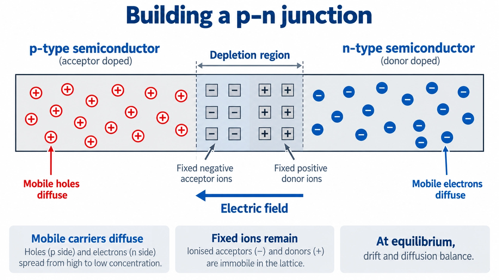
Bring p-type and n-type regions together within one crystal. Initially, electrons tend to diffuse from the electron-rich n-side into the p-side. Holes tend to diffuse in the opposite direction. Some carriers recombine near the boundary.
This leaves a region with relatively few mobile carriers and exposed fixed dopant charges: negative acceptor ions on the p-side and positive donor ions on the n-side. This is the depletion region. Its electric field points from the positive n-side towards the negative p-side.
That field opposes further majority-carrier diffusion. At thermal equilibrium, drift and diffusion currents balance, so there is no net current through the isolated junction. Carriers have not stopped moving; their opposing contributions balance.
Add a battery
Connect the p-side towards the positive terminal and the n-side towards the negative terminal: this is forward bias. It lowers the barrier to carrier injection. With suitable external circuitry, substantial current can flow.
Reverse the connection and the barrier increases. In the ordinary reverse-bias range, only a small leakage current flows in darkness. Light can add a photocurrent. At sufficiently high reverse voltage, breakdown mechanisms become important; these are not captured by “a diode blocks all reverse current”.
A silicon diode does not have one universal turn-on voltage. Its current–voltage curve is continuous, and the voltage at a chosen current depends on temperature and device construction. The familiar “about 0.7 V” is a convenient circuit approximation under some conditions.
For an ideal, non-degenerate silicon junction at equilibrium, Vbi = (kT/q) ln(NAND/ni²). Taking NA = ND = 1016 cm−3, ni = 1010 cm−3 and T = 300 K gives about 0.71 V.
This is an internal equilibrium potential difference. It is not a voltage source from which an isolated, uniform-temperature junction can continuously deliver energy. It is also not the threshold voltage of a transistor. [1][5][6]
From a junction to a solar panel, a camera and an LED
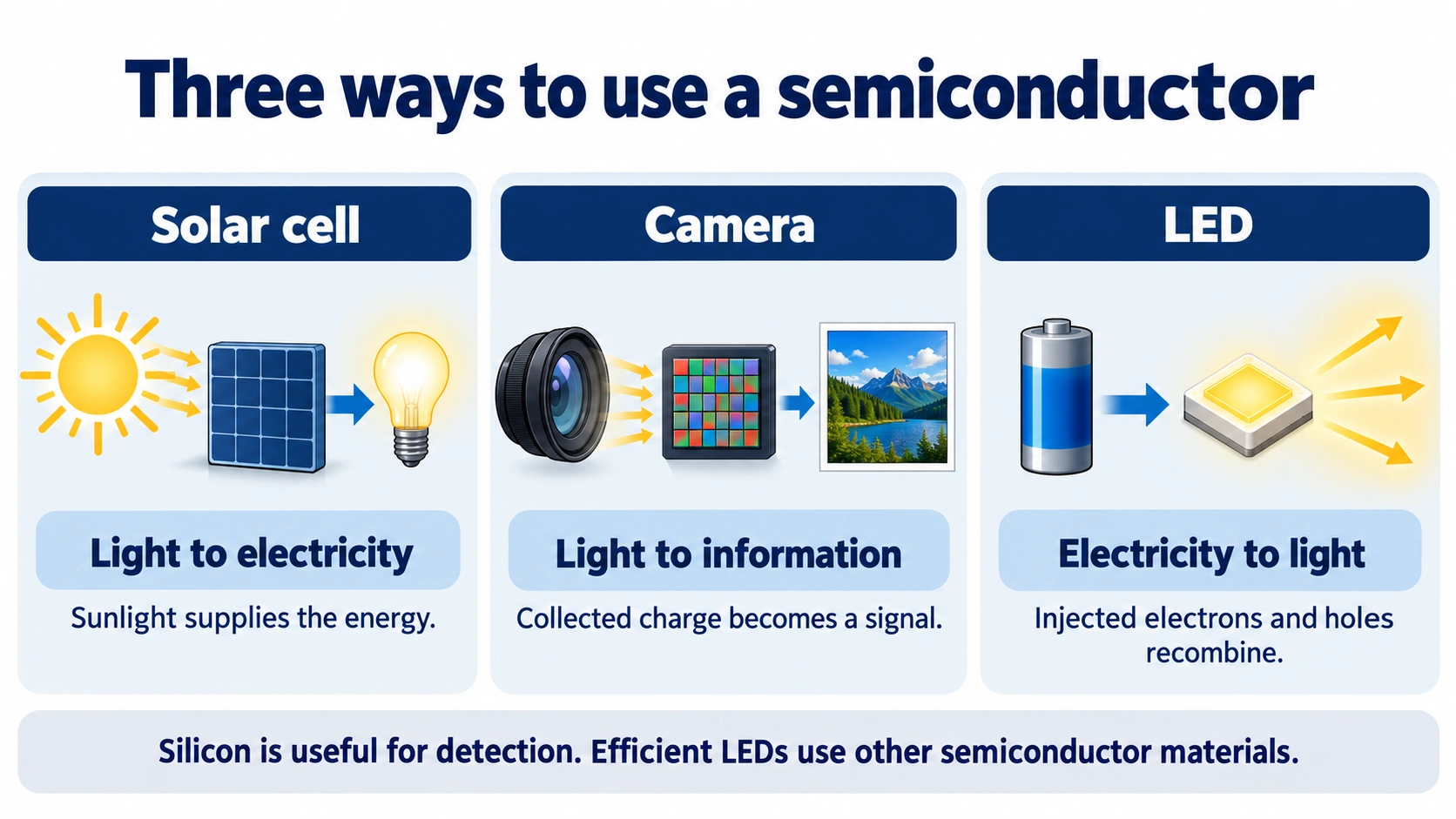
The same vocabulary now explains three familiar technologies. The important questions are: where do carriers come from, what separates or injects them, and where does the energy go?
A solar cell: collect energy carried by light
An absorbed photon can create an electron–hole pair. A junction and the surrounding device structure help separate and collect the carriers before they recombine. Electrons are collected towards the n-contact and holes towards the p-contact. Connect a suitable external load and the illuminated device can deliver electrical power.
The energy comes from the light. The internal field helps organise charge collection; it does not provide an inexhaustible energy supply. Losses arise when light is reflected or transmitted, when excess photon energy becomes heat, and when carriers recombine before collection. [7]
A camera sensor: count light well enough to form a picture
Each pixel contains a photosensitive structure. During an exposure, absorbed light generates charge that is collected and then read out as an electrical signal. Electronics convert the signal into digital values. In a typical colour sensor, filters help different pixels sample different parts of the spectrum, and processing reconstructs a colour image. [4][8]
More collected charge usually indicates more light, within the usable range. But a brighter pixel is not simply “one electron with more energy”. The useful signal is largely related to how much charge has accumulated.
Long exposures and warm sensors can reveal dark current: unwanted charge generated even without incoming light. This is one reason thermal behaviour matters in photography and scientific imaging. Photon statistics and readout electronics also contribute noise; cooling does not remove every source of uncertainty. [4]
An LED: inject carriers and let them release light
In a light-emitting diode, electrical energy drives electrons and holes into an active region. They can recombine and release energy as photons. A transition energy around 2 eV corresponds to roughly 620 nm, in the orange-red region; around 2.8 eV corresponds to roughly 443 nm, in the blue region. These are illustrative conversions, not specifications for every LED. [9]
Why not use ordinary silicon for all our LEDs? Silicon has an indirect band gap. Efficient radiative recombination requires a change in both energy and crystal momentum, with lattice vibrations participating in the process. In a suitable direct-band-gap material, the momentum requirement is simpler and light emission can be much more efficient. Silicon absorbs useful light well enough for many detectors, yet is a poor choice for a conventional efficient light emitter. Absorption and emission are not equally convenient engineering tasks. [1][9]
Actual blue LEDs commonly use indium gallium nitride active layers within a more complex structure. Their colour is set by the active region, including its composition and quantum-well design; it cannot be inferred simply from the bulk band gap of gallium nitride. A common white LED combines blue emission with a phosphor that converts some of the light to longer wavelengths. The mixture looks white. [9][10]
A detector needs to absorb the wavelengths of interest. An emitter needs an efficient route for electrical energy to become photons of the desired colour. A power switch must block voltage and manage losses. “Larger band gap” does not mean “better semiconductor” without a particular job in mind.
The transistor: use one voltage to control another current
A diode gives us a junction. A transistor adds a powerful new capability: a relatively small control signal can govern a conducting path. This makes amplification and switching possible.
For modern logic, a useful starting example is the MOSFET: metal–oxide–semiconductor field-effect transistor. The historical name remains useful even though modern gate stacks can use more complicated materials.
Consider an n-channel MOSFET, or nMOS. It has a source, a drain and a gate. An insulating layer separates the gate from the semiconductor. With suitable source, drain and body voltages, raising the gate voltage above a threshold creates an electron-rich conducting channel between source and drain.
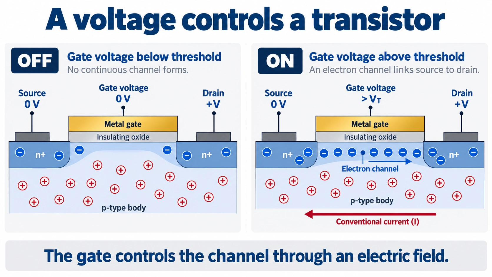
The gate controls the channel through an electric field across the insulating layer. In the ideal steady state, electrons do not flow continuously through that oxide from the gate into the channel. Real devices have leakage, and changing the gate voltage requires charging or discharging capacitance.
The source supplies the electrons that move along the channel. The gate does not need to create every conducting electron by lifting it across the full silicon band gap. This is another reason to keep the ideas of carrier generation and carrier transport separate.
A p-channel MOSFET, or pMOS, uses a complementary arrangement and holes as its principal channel carriers. Its voltage conditions are different; it should not be imagined as an nMOS with only the arrow reversed.
How switching becomes a logical decision
In a simple CMOS inverter, a pMOS device connects the output towards the positive supply and an nMOS device connects it towards ground. Their gates share an input.
| Input condition | Upper pMOS | Lower nMOS | Output condition |
|---|---|---|---|
| Low voltage, interpreted as 0 | On | Off | Pulled high, interpreted as 1 |
| High voltage, interpreted as 1 | Off | On | Pulled low, interpreted as 0 |
The output is a voltage that can control the gates of the next stage. A low output is a valid signal, not “no information” and not a command for the next circuit to stop. Circuits assign meanings to voltage ranges and combine many such operations to represent numbers, instructions and images. [11]
In an ideal stable state, one transistor is off, so there is no direct conducting path from the supply to ground. During switching, capacitances charge and discharge; there can also be a brief current while both devices partly conduct. Real circuits additionally have leakage. A phone that becomes warm while processing video is showing the cumulative effect of electrical losses across a very large circuit, not heat from one single electron jumping a band gap. [11]
A common first estimate for dynamic logic power is P ≈ αCV²f: activity factor α, switched capacitance C, supply voltage V and switching frequency f. Under the assumptions of this model, doubling frequency doubles dynamic power; reducing voltage helps strongly because voltage is squared.
This is not the whole power budget. Leakage, short-circuit current, memory access, interconnect and other parts of a system also matter. Raising frequency may require a higher voltage, so real power can rise faster than this simple frequency comparison suggests. [11]
From one transistor to an integrated circuit
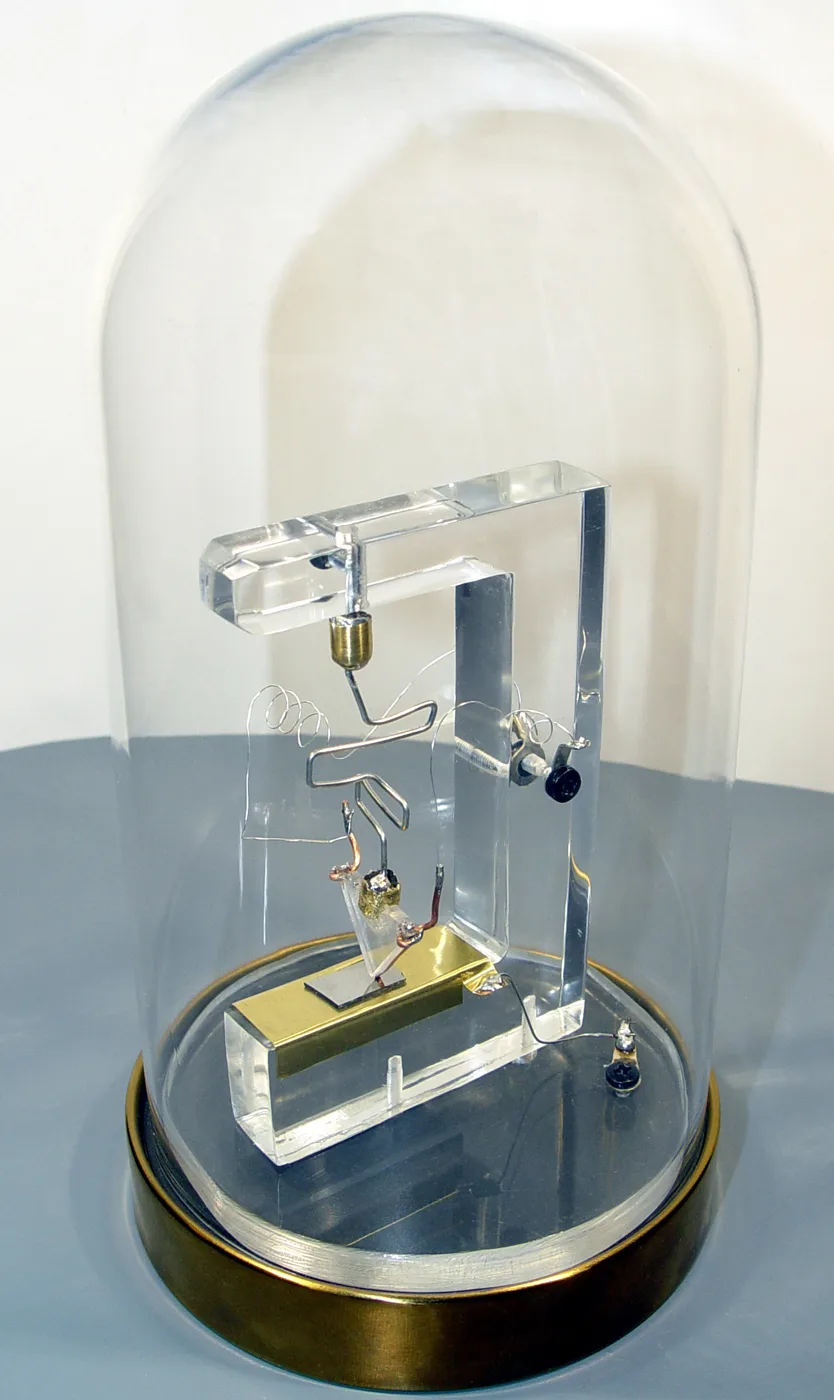
The first working point-contact transistor was demonstrated at Bell Labs in 1947. It used germanium and looked nothing like today's flat, densely patterned chips. It established that a solid-state device could control and amplify an electrical signal. The 1956 Nobel Prize in Physics recognised the transistor work of John Bardeen, Walter Brattain and William Shockley. [12][13]
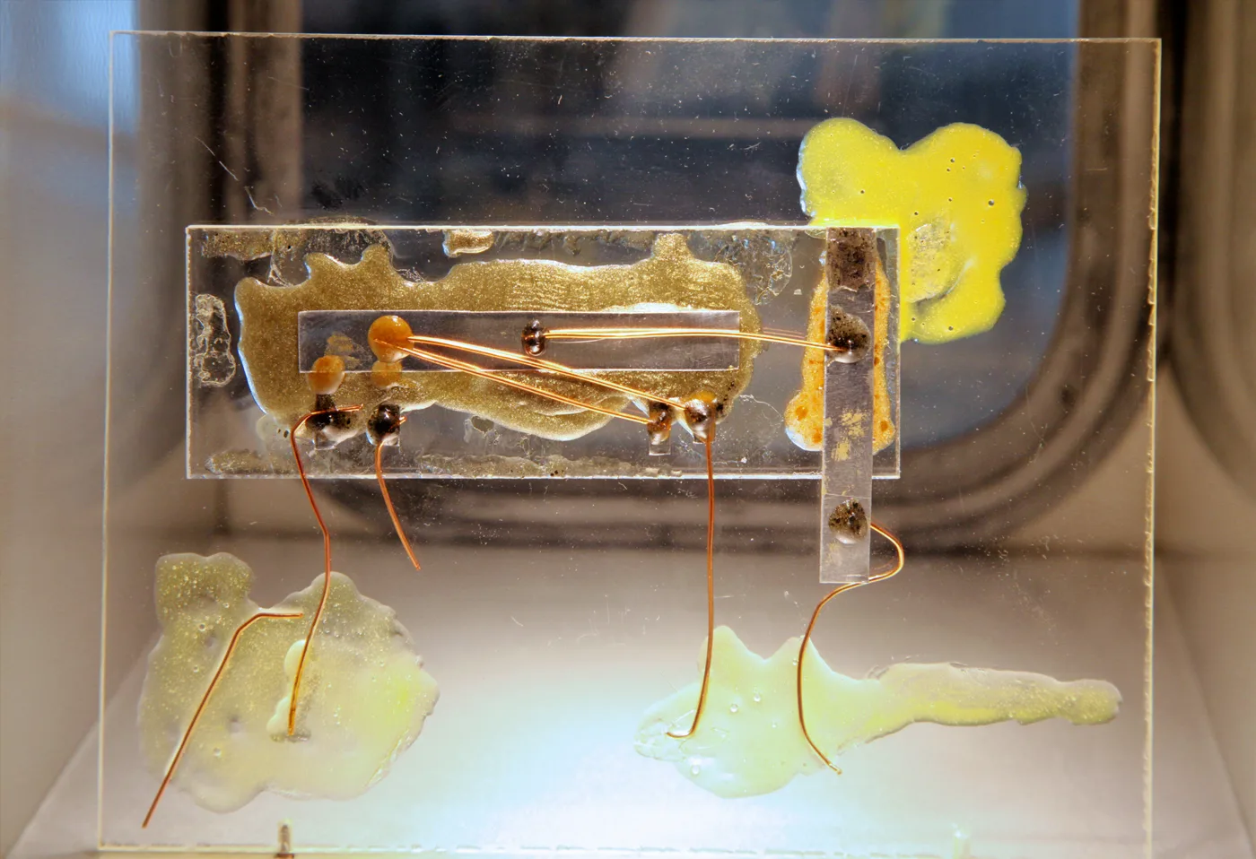
A further breakthrough was to make multiple components and connections as an integrated circuit. Jack Kilby demonstrated an early integrated circuit in 1958; Robert Noyce's work on a practical monolithic approach helped establish the route towards manufacturable silicon ICs. Integration reduced the need to assemble and wire every component individually. [14][15]
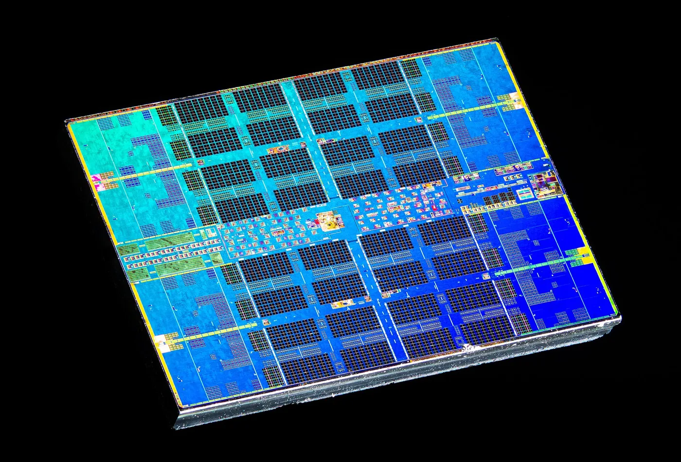
Today, the visible rectangles in a chip photograph are functional blocks and repeating circuit patterns, not a convenient photograph of every individual transistor. A chip contains devices, insulating layers, contacts and many levels of metal wiring. The wiring is as essential as the switches it connects.
Why making transistors smaller becomes difficult
Smaller devices can allow more functions within a given area and can reduce some capacitances. But as the channel becomes very short, the drain can interfere more strongly with the gate's control. Leakage, variability, resistance and heat become increasingly difficult to manage.
This helps explain the move from planar transistors to FinFETs, where the gate controls a raised fin from several sides, and gate-all-around structures, where it surrounds narrow channels. The purpose is better electrostatic control, not merely a more elaborate shape. [16][17]
A technology label such as “3 nm” is the name of a process generation. It should not be treated as a ruler reading for every transistor gate, wire or other feature. Comparing processes requires actual device and circuit metrics, not just the smallest number in a product announcement. [18]
What fabrication has to achieve
The physics tells us what a device needs. Fabrication turns that requirement into a repeatable structure across a wafer.
| Device requirement | What manufacturing must control |
|---|---|
| A predictable crystal | Purity, crystal quality and defects |
| Selected electron-rich and hole-rich regions | Dopant species, dose, depth and activation |
| A gate that controls a channel | Film thickness, interface quality and gate geometry |
| Insulation between conducting regions | Dielectric quality and patterning |
| Electrical access to devices | Contacts, metal wiring and alignment |
| Many devices that behave consistently | Contamination, process variation and measurement |
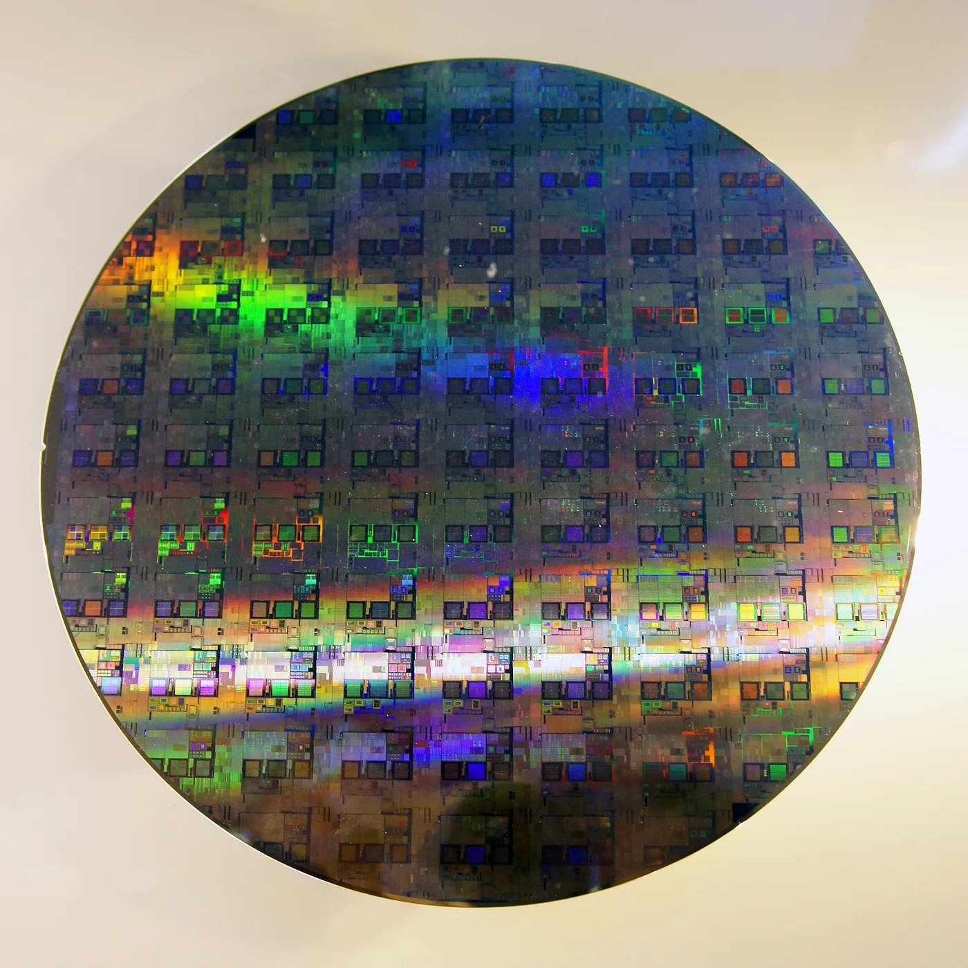
A wafer is not a single enormous transistor. It is the working surface on which many chips are fabricated in parallel. After processing and testing, chips are separated and packaged so that they can be connected to the outside world.
When later chapters introduce oxidation, deposition, lithography, etching or ion implantation, connect each process to the structure it creates. A gate oxide matters because it must insulate while allowing field control. A doped region matters because it supplies carriers and establishes electrical boundaries. A metal contact matters because a useful device must exchange charge with a real circuit.
The central thread is control: control of available states, carrier populations, electric fields, interfaces and geometry. From that control come the camera, the logic circuit and the power switch.
Check your understanding
Why is “a material between a conductor and an insulator” an incomplete explanation?
Show answer
It describes a possible conductivity range but misses controllability. Doping, fields, light and temperature can change carrier populations or transport, making useful devices possible.
Does the band gap describe a physical distance between two layers?
Show answer
No. It is a forbidden energy range between allowed bands in a bulk crystal. Vertical position on an energy-band diagram represents energy.
Must every electron cross the full band gap each time a transistor switches?
Show answer
No. A gate can control the movement of existing carriers within a channel. Carrier generation and carrier transport are different processes.
A hole moves right. In the seat analogy, which way do the electrons filling the vacancy move?
Show answer
Left. Tracking the vacancy gives a useful description of transport without following every valence electron.
Electrons drift left and holes drift right. Can they contribute to current in the same direction?
Show answer
Yes. Conventional current points in the direction positive charge would move, so both contributions here point right.
Is n-type silicon necessarily a negatively charged object?
Show answer
No. In a nearly neutral region, mobile electrons are balanced by positive ionised donor atoms. The label identifies the majority carrier type.
What establishes the depletion region's electric field?
Show answer
Fixed ionised dopants left behind as mobile carriers redistribute: negative acceptors on the p-side and positive donors on the n-side.
Where does a solar cell's output energy come from?
Show answer
Incoming light. The device's internal field and structure help separate and collect carriers; they are not a limitless energy source.
Why can silicon work well in a camera but poorly as a conventional efficient LED?
Show answer
It can absorb useful light and generate collectable charge, but its indirect band gap makes efficient radiative recombination less convenient than in suitable direct-gap materials.
Does a MOSFET gate normally supply the channel's steady current through its oxide?
Show answer
No. The gate controls the channel through an electric field. The source supplies carriers; gate capacitance must be charged when the control voltage changes, and real devices have leakage.
Does a logic 0 mean that a circuit has no information?
Show answer
No. Low and high voltage ranges are both valid logical states. A low output can cause the following stage to produce a high output.
Does a “3 nm” process mean that every gate and wire measures 3 nm?
Show answer
No. It is a process-generation label. Individual dimensions and performance metrics must be checked separately.
A short glossary
- Band gap
- The forbidden energy range between relevant allowed electronic bands.
- Carrier
- A mobile charge described as an electron or a hole.
- Conduction band
- An allowed band in which electrons can contribute to conduction.
- Valence band
- The band associated with bonding electrons; holes in it can contribute to conduction.
- Doping
- Deliberately introducing selected impurities to control electrical behaviour.
- Donor / acceptor
- A dopant that supplies an electron / accepts an electron and leaves a hole.
- Majority carrier
- The more abundant carrier type in a doped region.
- Drift
- Average carrier movement driven by an electric field.
- Diffusion
- Net carrier movement associated with a concentration gradient.
- Recombination
- The removal of an electron–hole pair through an allowed transition process.
- Depletion region
- A junction region depleted of many mobile carriers, with fixed dopant charge.
- Bias
- An externally imposed electrical operating condition, usually specified by voltages.
- MOSFET
- A transistor whose insulated gate controls a semiconductor channel through an electric field.
- CMOS
- Complementary circuitry using n-channel and p-channel MOS transistors.
- Wafer
- A thin semiconductor disc used as a substrate for device fabrication.
- Die
- One individual chip before or after separation from a wafer.
Sources and further reading
The sources below support the physical data, device explanations and historical examples. Numerical estimates in the text state their assumptions. Band diagrams, carrier symbols and device cross-sections are explanatory models, not atomically accurate images. Material parameters vary with temperature, doping and measurement method. This introduction deliberately leaves out advanced transport, detailed quantum-well physics and full circuit design.
- Ioffe Institute — Silicon: material properties and band structure — https://www.ioffe.ru/SVA/NSM/Semicond/Si/
- National Bureau of Standards — Copper Wire Tables, Handbook 100 — https://nvlpubs.nist.gov/nistpubs/Legacy/hb/nbshandbook100.pdf
- NIST — CODATA: lattice parameter of silicon — https://physics.nist.gov/cgi-bin/cuu/Value?asil
- Hamamatsu Photonics — Si photodiodes: technical information — https://www.hamamatsu.com/content/dam/hamamatsu-photonics/sites/documents/99_SALES_LIBRARY/ssd/si_pd_kspd9001e.pdf
- NIST — Boltzmann constant in eV/K — https://physics.nist.gov/cgi-bin/cuu/Value?kev
- MIT OpenCourseWare — Microelectronic Devices and Circuits: carrier drift and diffusion — https://ocw.mit.edu/courses/6-012-microelectronic-devices-and-circuits-spring-2009/4692cf463514c4f47d8629fab7d41c15_MIT6_012S09_lec03.pdf
- US Department of Energy — Solar Photovoltaic Cell Basics — https://www.energy.gov/cmei/systems/solar-photovoltaic-cell-basics
- Sony Semiconductor Solutions — Image sensor technology — https://www.sony-semicon.com/en/technology/is/index.html
- Toshiba — Basics of discrete semiconductors: LEDs — https://toshiba.semicon-storage.com/content/dam/toshiba-ss-v3/master/en/semiconductor/knowledge/e-learning/discrete/discrete-basic-chap5_en.pdf
- Nichia — The story of the white LED — https://led-ld.nichia.co.jp/en/blog/m000012.html
- Texas Instruments — CMOS Power Consumption and Cpd Calculation — https://www.ti.com/lit/an/scaa035b/scaa035b.pdf
- Computer History Museum — Invention of the Point-Contact Transistor — https://www.computerhistory.org/siliconengine/invention-of-the-point-contact-transistor/
- Nobel Prize — The Nobel Prize in Physics 1956 — https://www.nobelprize.org/prizes/physics/1956/summary/
- Computer History Museum — Kilby's first integrated circuit — https://www.computerhistory.org/tdih/september/12/
- Computer History Museum — Practical Monolithic Integrated Circuit Concept Patented — https://www.computerhistory.org/siliconengine/practical-monolithic-integrated-circuit-concept-patented/
- Intel — Transistor backgrounder: the move to 3-D Tri-Gate transistors — https://download.intel.com/newsroom/kits/22nm/pdfs/Intel_Transistor_Backgrounder.pdf
- Samsung Semiconductor — Chip production using gate-all-around architecture — https://semiconductor.samsung.com/news-events/news/samsung-begins-chip-production-using-3nm-process-technology-with-gaa-architecture/
- IEEE Spectrum — A Better Way to Measure Progress in Semiconductors — https://spectrum.ieee.org/a-better-way-to-measure-progress-in-semiconductors
Written and reviewed for the English edition, 31 October 2026. Numerical examples are illustrative unless stated otherwise.
Original explanatory illustrations generated with OpenAI Image Gen for this English edition. Third-party photographs retain their stated licences; image credits accompany each photograph.