COMPANY PROFILE / ADHESIVES & ENCAPSULANTS
ams OSRAM
— A photonics device maker, seen from the buying side of adhesives and encapsulants
ams OSRAM makes optical semiconductors (LEDs, lasers and light sensors) and is headquartered in Austria, with a co-headquarters in Germany. It is not an adhesives or encapsulants maker. It sits on the customer side: it uses those materials when it builds LEDs and sensors. This profile draws on the company's annual report, its application notes and its product datasheets to set out how it uses and chooses encapsulants, adhesives and silicones in LED packages. What the published sources do not tell us is which materials suppliers it buys what from, in what volumes, or whether it formulates any materials itself. We say so plainly in Chapters 1 and 5 and do not fill the gap with guesses.
- ams OSRAM in 30 seconds, and where it stands in adhesives and encapsulants
- The logo and how the name is written
- Where the company sits in adhesives and encapsulants
- Scale
- Resources committed to adhesives and encapsulants
- What it has done so far
- What comes next
- What the company is aiming for in adhesives and encapsulants
- Map of partnerships in adhesives and encapsulants
- Technologies, products and services
- The risks this company carries
- Glossary / References / Claim-to-source audit
1. ams OSRAM in 30 seconds, and where it stands in adhesives and encapsulants
ticker AMSPublished its 2025 annual report on 20 March 2026
(optical semiconductor maker)Fits none of the three types; the closest is semiconductor & electronic materials
hybrids, glassFor encapsulation and lenses. Die-attach adhesives and others (application note AN122)
In-house formulationNot stated in the annual report or application notes
Companies in adhesives and encapsulants fall into three broad types: general adhesives & chemicals makers, semiconductor & electronic materials makers, and UV-curing & specialty makers. ams OSRAM fits none of them, because it does not make and sell adhesives or encapsulants; it uses them in its LED and sensor products. Figure 1 highlights the closest type, semiconductor & electronic materials, and says so in a note. The company's annual report lists the main manufacturing steps as including "chip assembly, encapsulation and coating, and calibration and final testing", and names among the materials it buys "connecting materials made of ceramics, plastics, epoxy resins, and silicones" Sourced. Application note AN122 (2018) explains that LED encapsulants are chosen from epoxy, epoxy/silicone hybrid, silicone and glass, and that the guide for choosing is "thermal stability, transmission performance, gas/humidity permeability and refractive index match" Sourced.
What the sources we reviewed do not say is which company's products it uses, in what quantities, or what in-house formulation and evaluation it does Not yet confirmed. This article therefore concentrates on "what criteria a materials user applies, and what it treats as the trouble spots", and is explicit that what can be confirmed is limited.
Decision to write this profile: we judged that it should be written. Four primary sources of the company's own contain concrete facts on encapsulation and bonding materials (processes, material classes, the trade-offs between materials, test conditions and handling cautions): the 2025 annual report, application note AN122, application note AN024 and an LED datasheet. Information on procurement and formulation is thin, however, so what can be confirmed stops at "how the materials are used and chosen".
2. The logo and how the name is written

A note on naming: the legal entity is ams-OSRAM AG and the group is ams OSRAM. On their covers, AN122 (2018) is issued under the name "OSRAM Opto Semiconductors", while AN024 (2022) and the 2023 datasheet are issued under "ams-OSRAM AG" Sourced. In other words, the older technical documents cited here were written by a unit that is the predecessor of today's ams OSRAM (we did not review the details of how the names were merged).
The logo is the one shown on the front page of the company's official website (an SVG file), saved as
img/ams_osram_logo.svg. It is not AI-generated.
3. Where the company sits in adhesives and encapsulants
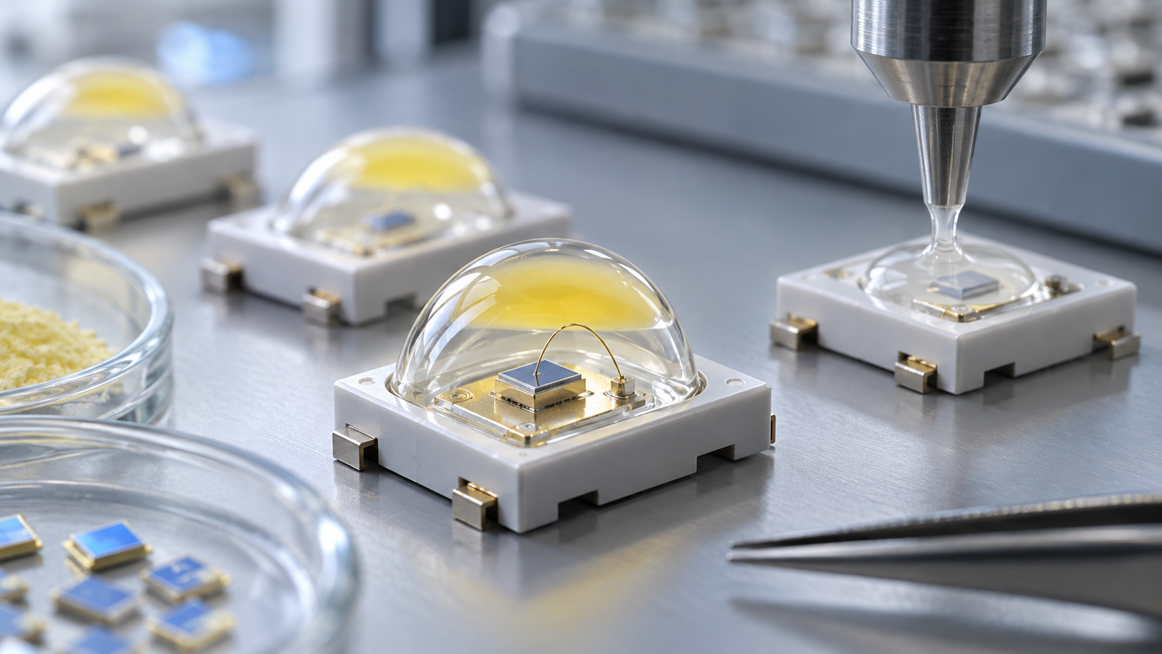
An LED package uses adhesive and encapsulating materials in at least four places. The table restates AN122's cross-section of an LED in our own words.
| Part | Role | Material (as described in AN122) |
|---|---|---|
| Die attach (fixing the chip) | Fixes the chip to the lead frame | Either glued with an adhesive or soldered. Silver or gold particles may be added to the adhesive to raise electrical conductivity |
| Housing (outer shape) | Gives the package its shape, acts as a reflector to extract light, and protects against external force | Thermoplastic polymer, silicone or epoxy. Some packages use ceramic substrates (for example the OSLON family) |
| Encapsulant and lens | Protects the chip and lead frame, buffers stress, reduces light-coupling losses and sets the beam pattern. Phosphor can be mixed in to convert color | Epoxy, epoxy/silicone hybrid, silicone or glass |
| Phosphor (color conversion) | Converts the blue chip's light into yellow and other colors to make white | Either dispersed through the encapsulant, or applied as a thin conversion layer on the chip surface (chip-level coating) |
4. Scale
The table gives the scale of the whole company. Figures for adhesives and encapsulants alone are not published Sourced.
| Measure (EUR million) | 2024 | 2025 |
|---|---|---|
| Revenue (group) | 3,428 | 3,323 |
| Opto Semiconductors (OS: LEDs, lasers and other emitters) | 1,448 | 1,375 |
| CMOS Sensors and ASICs (CSA: optical sensors and analog ICs) | 981 | 1,010 |
| Lamps & Systems (L&S: lamps and lighting) | 1,000 | 938 |
| Research and development expenses | 419 | 388 |
| Investments in intangible assets and property, plant and equipment (after government grants) | 502 | 117 |
| Item | Detail |
|---|---|
| Employees | 19,120 at the end of 2025 (19,665 at the end of 2024). The company's releases of May to July 2026 say "approximately 18,500" |
| Manufacturing | 16 production sites and two test sites (end of 2025), including Premstaetten (Austria), Regensburg and Herbrechtingen (Germany), Singapore, Wuxi (China), and Penang and Kulim (Malaysia) |
| R&D sites | 25 large development hubs worldwide. LED development is in Germany and Malaysia; development of packaging and conversion (phosphor) solutions is spread across Austria, Germany, Malaysia, China and Singapore |
| Patents | About 12,100 patents and applications (about 4,600 patent families) |
| April-June 2026 | Revenue EUR 805 million; adjusted EBITDA margin 16.9% (company announcement) |
Revenue in 2025 fell about 3% from the previous year, according to the company. The annual report attributes the decline at OS to inventory corrections by automotive LED customers, a cyclical low in industrial demand and a weaker U.S. dollar. R&D expenses were 12% of revenue, the same share as the year before. How much of revenue goes on encapsulating and bonding materials is not disclosed Not yet confirmed.
The OS segment's revenue (EUR 1,375 million) covers all emitters, such as LEDs and lasers; it is not a figure for packaging (encapsulation and bonding). The group's R&D spending of EUR 388 million likewise covers everything, including sensors, IC design and software. The purchase value of encapsulating and bonding materials, R&D spending on them, and dedicated headcount are all undisclosed, and this article does not estimate them. The sustainability report does give the total weight of direct materials the group used (23,990 tonnes in 2025), but it does not break that down (the amounts of epoxy, silicone and so on).
5. Resources committed to adhesives and encapsulants
The table covers four points (people, money, external deals, and public or academic links) and separates what we could confirm from what we could not. An explicit "no mention" is a finding in its own right.
| Type of resource | Confirmed | Not confirmed | Status |
|---|---|---|---|
| People and sites | Average R&D headcount for the group was 2,544 in 2025 (2,783 in 2024). The company has 25 large development hubs. Development of packaging and conversion (phosphor) solutions is spread across Austria, Germany, Malaysia, China and Singapore. "Encapsulation and coating" is one of the manufacturing steps it runs itself | Dedicated R&D headcount for encapsulating and bonding materials | Sourced / not disclosed |
| Money | R&D expenses of EUR 388 million (12% of revenue). Investments in intangible assets and property, plant and equipment of EUR 117 million (after grants). Direct materials totaled 23,990 tonnes in 2025 (including epoxy resins and silicones; no breakdown) | Purchases of encapsulating and bonding materials, and R&D spending on them | Sourced / not disclosed |
| Investments, acquisitions, joint ventures, divestments | Mainly divestments. It spun off its passive optical components business in the second half of 2024, announced the sale of its entertainment and industry lamps business in July 2025, agreed in February 2026 to sell its non-optical analog/mixed-signal sensor business to Infineon (EUR 570 million; completed 1 July 2026), and agreed in May 2026 to sell its CMOS image sensor business to indie Semiconductor (EUR 40 million, according to the company) | Any investment in, acquisition of, joint venture with or long-term supply contract with an encapsulant or adhesive maker (none stated) | Sourced / not confirmed |
| Universities, research institutes, public funding | Its development teams, together with those of Fraunhofer IZM (a German research institute), won the German Future Prize 2024 (Digital Light) for the multi-pixel LED EVIYOS. In 2025 it received EUR 83 million of funding from the European Commission's European Chips Act (the annual report says the Republic of Austria funds the new Premstaetten factory for CMOS sensors under that act) | Joint research with universities or institutes, or grants, on encapsulating and bonding materials (none stated). The funding above is for a CMOS-sensor factory, not for encapsulant development | Sourced / not confirmed |
AN122 says its LEDs undergo robustness tests per JEDEC JESD22-A108 (steady-state life) and 101 (temperature and humidity), that the company runs its own corrosion test at 15 ppm hydrogen sulfide, 40 °C and 90% relative humidity for more than 1,000 hours (stating that no recognized international standard exists for it), and that it also uses EN 60068-2-60 Method 4 (25 °C, 75% relative humidity, 200 ppb SO2, 200 ppb NO2, 10 ppb H2S and 10 ppb Cl2 for 21 days) Sourced. A materials maker guarantees the properties of a single material, but how a package behaves when the chip's heat and light, moisture and outside chemicals act together is something only the user can know. ams OSRAM's notes pass that knowledge on to customers, and they carry many cautions for the people who choose encapsulants, adhesives and coatings (luminaire makers). They can be read as a view of the same phenomena from the opposite side to the explainers on materials makers in this series.
6. What it has done so far
| When | What happened | Why it matters |
|---|---|---|
| 6 August 2018 | Issued application note AN122, "Chemical compatibility of LEDs" (under the name OSRAM Opto Semiconductors). It sets out the mechanisms of encapsulant discoloration, lead-frame sulfidation and phosphor degradation, plus test methods and a materials compatibility list | A systematic guide for customers on choosing encapsulating and bonding materials |
| 15 November 2022 | Issued application note AN024, "Handling of silicone resin LEDs". It says the company aims at a lifetime of 100,000 hours at room temperature for very bright LEDs and adopted a silicone sealing compound | Publishes why it uses silicone encapsulant, and handling cautions |
| 29 September 2023 | Datasheet (version 1.7) for the white LED "OSLON Black LCW H9GP": "SMD epoxy package with silicone lens", corrosion robustness class 3B, AEC-Q102 qualified, and so on | A real product that combines epoxy and silicone |
| 2024 | EVIYOS (multi-pixel LED) won the German Future Prize with Fraunhofer IZM. The passive optical components business was spun off in the second half | Concentration on high-value products, and tidying of non-core activities |
| 2025 | Ramped up production of EVIYOS HD25 (25,600 pixels). Improved ALIYOS (LED-on-foil) with thin, transparent and 2.5D-bendable versions. Throughout the year it pursued the debt-reduction plan outlined in April (aiming for well over EUR 500 million of divestment proceeds) | Package forms are diversifying |
| February 2026 | Announced a strategy to lead in "Digital Photonics" and the "Simplify" restructuring program (below) | Narrowing of the business |
| 1 July 2026 | Completed the sale of its non-optical sensor business to Infineon. Set up Digital Photonics business lines | A change in the scope of the company through divestment |
7. What comes next
mid-to-high single digitsAdjusted EBITDA margin of at least 25%. A company target (not yet confirmed)
over EUR 200 millionLeverage below 2. A company target
a year by end of 2028Plans to cut just over 2,000 jobs over three years. A company plan
The company says it will focus its European sites on "innovative and distinctive products" and make standardized, cost-intensive products mainly in Asia ("Simplify", announced 10 February 2026, per the annual report). The plan includes moving some production and R&D Not yet confirmed. It names automotive, AR (augmented-reality) smart glasses, biosensing, robotics and AI data-center optical interconnects as growth targets Sourced.
None of the following appears in the primary sources we reviewed Not yet confirmed.
Development plans, planned materials or supplier changes for packaging encapsulants and adhesives; the outlook for materials purchases; and how encapsulation and bonding processes or material specifications will change with the production moves under "Simplify". Research-firm estimates are not used here because they do not come from the company itself.
8. What the company is aiming for in adhesives and encapsulants
This chapter includes points the company does not state directly. They are inferences from primary sources, set out with their grounds.
| What can be read | Primary-source basis | Status |
|---|---|---|
| For uses that put a premium on lifetime, heat resistance and light resistance (above all automotive), encapsulant choice leans toward silicone | AN024 says housings using silicone resin allow a higher junction temperature than epoxy-based ones, show high moisture and cycling reliability, and are well suited to the automobile industry. The annual report says automotive is the largest end market and OS is the global leader in automotive LEDs | Inference |
| But it does not use silicone alone; it mixes materials according to the application | The datasheet lists a product with an "epoxy package with silicone lens". AN122 says it offers LED packages with epoxy, hybrid and silicone encapsulants | Sourced |
| It treats many material failures as problems of the customer's installation and surrounding materials | AN122 lists in detail the compatibility of conformal coatings, sealants, adhesives, cleaning agents, gaskets and more that customers use, and says "sufficient customer testing is always necessary" | Sourced |
| Moving standardized production to Asia could also change how materials are sourced and qualified | "Simplify" sets a policy of making standardized products mainly in Asia. Nothing is said about the effect on materials | Inference (weak grounds) |
The first inference rests on AN024. It says an LED's lifetime is determined not by the semiconductor chip itself but primarily by the housing (package), and that to reach a lifetime of 100,000 hours (the time for brightness to fall to half, at room temperature) in very bright LEDs the company adopted a silicone sealing compound Sourced. AN122 adds an example of epoxy encapsulation yellowing under blue light and heat, with silicone keeping its light output better in a 1,000-hour test at 85 °C and 85% relative humidity (30 mA). From this it is reasonable to read that the higher the power, temperature and blue-light exposure, the more likely silicone is chosen. But no list of which product uses which material has been published, so this is our interpretation Not yet confirmed.
9. Map of partnerships in adhesives and encapsulants
10. Technologies, products and services
What ams OSRAM sells is not materials but optical semiconductors built with them. This chapter therefore uses its application notes and product datasheet to set out how it uses encapsulating and bonding materials, and the criteria it applies in choosing them. The values are the manufacturer's (ams OSRAM's) stated values or test examples, and cannot be compared across different grades or conditions.
Choosing between epoxy and silicone (AN122's summary)
| Item | Epoxy | Silicone |
|---|---|---|
| Strengths | Hard, with good mechanical protection; good thermal-expansion match to LEDs; good adhesion to housing and lead frame; low gas and humidity permeability; lower price; refractive index about 1.5 | Withstands high power; high thermal stability (allows a higher junction temperature) |
| Weaknesses | Limited thermal stability; weak against light, especially blue light. Yellows through thermal oxidation | Soft, low stiffness; high thermal expansion; tacky surface that attracts dust; high gas and humidity permeability; higher price; refractive index 1.4-1.5 |
| How it degrades | A three-dimensional network cured with an anhydride hardener. Heat and light break bonds in the backbone, and the cleaved aromatic groups cause the discoloration | Si-O backbone. Oxidation of methyl groups adds crosslinks, so the material hardens and cracks. Cleaved phenyl groups can form chromophores and cause discoloration |
Hybrids, with properties between epoxy and silicone, are also used. AN122 gives the guide for choosing an encapsulant as "thermal stability, transmission performance, gas/humidity permeability and refractive index match" Sourced.
Product example and datasheet statements
| Document / product | Statement (manufacturer's stated) | Conditions / standards | Date |
|---|---|---|---|
| OSLON Black LCW H9GP (white LED) | Package "SMD epoxy package with silicone lens"; corrosion robustness class 3B; AEC-Q102 qualified; moisture sensitivity level MSL 2; not suitable for ultrasonic cleaning | Corrosion test: 40 °C, 90% relative humidity, 15 ppm H2S, 14 days (stated to be stricter than IEC 60068-2-43). MSL per JEDEC J-STD-020E | Version 1.7, 29 September 2023 |
| Type-designation key in the same datasheet | Encapsulation options include "silicone encapsulation (casted)" and "planar compression molded silicone" (with volume or layer conversion) | Conversion = color conversion by phosphor | Same |
| AN024 (silicone resin LEDs) | Adopts a silicone sealing compound and aims at a lifetime of 100,000 hours (room temperature) for very bright LEDs; a material with an extremely low level of volatile content; suitable for automotive use; clean with isopropyl alcohol for 5-10 seconds (15 at most); ultrasonic cleaning not recommended | Lifetime = time for brightness to fall to half of its initial value | 15 November 2022 |
AN024 says silicone is generally softer than standard encapsulants and its surface is more likely to attract dust. It therefore asks users to clean after soldering where needed, not to pierce the sealing compound with sharp objects, and to choose a pick-and-place nozzle larger than the reflector area Sourced. It also says that small foreign particles on the surface, though noticeable cosmetically, do not affect quality, lifetime or brightness and can be ignored.
The most practical part of AN122 is its account of interactions with other materials around the LED Sourced.
(1) Silver sulfidation. A silver-plated lead frame reflects well, but it reacts with hydrogen sulfide and similar gases to form black silver sulfide, and the note says light output can fall by as much as 30-40%. It asks users not to place sulfur-containing vulcanized rubber (O-rings, gaskets) or sealants containing sulfur compounds near LEDs. Because silicone is permeable to gas and humidity, the route that matters is outside gas passing through the encapsulant to reach the silver. Epoxy is less permeable and suits protecting silver.
(2) Discoloration by volatile organic compounds (VOCs). When VOCs from adhesives, solder pastes, sealants, polyurethane potting and similar sources are trapped in a nearly airtight space (under a coating, inside a sealed luminaire), heat and light break them down on the chip surface into a thin dark layer, which lowers light output and shifts color. The note gives examples where, once the cause was removed and the LED kept running (under 100 hours), the discoloration largely reversed. It advises making coatings and sealants not too airtight, leaving room for the gas to escape.
(3) Cautions on silicone itself. AN122's chemical list says of silicones (sealants, adhesives, encapsulants, potting and coating resins): "depending on the silicone source, grade and curing condition, may cause package failure. Curing by-products during silicone curing may cause package contamination. Electronics material grade with low ionic and impurity content is highly recommended." It also notes that acetone may swell a silicone encapsulation, that tetrachloromethane may soften and tarnish it, and that toluene and xylene may interact with silicones. Read together with our explainers on silicones, automotive silicones and encapsulants, die attach and semiconductor encapsulants, it becomes clear why a user needs the "low volatiles" and "low ionic content" that materials makers advertise.
11. The risks this company carries
| Risk | Detail | Status |
|---|---|---|
| Financial burden | Interest-bearing loans and borrowings were EUR 2,561 million at the end of 2025. Bonds due 2029 carry 10.50% (euro) and 12.25% (U.S. dollar). The company has made deleveraging a key strategic focus | Sourced |
| A changing business scope | Divestments continue: non-optical sensors (Infineon), CMOS image sensors (indie Semiconductor), and lamps. The mix and specifications of packaging-material purchases could change as a result (the size of the effect is not disclosed) | Inference |
| Precious-metal and critical raw-material prices | Higher prices for gold and other precious metals pushed up costs in 2025. The report says the materials it buys include precious metals (gold, platinum, palladium), and AN122 mentions lead-frame plating such as NiPdAu, NiAu and silver. The split by process and quantity is not disclosed | Sourced |
| Concentrated suppliers | For critical materials it generally vets at least one secondary source besides the preferred vendor, but this is not always possible. It lists remaining dependence on suppliers based in Taiwan as a risk | Sourced |
| Swings in automotive and industrial demand | In 2025, OS revenue fell on inventory corrections by automotive LED customers and a cyclical low in industrial demand | Sourced |
| Customer-side material incompatibility | Incompatible conformal coatings, sealants, adhesives and cleaning agents that customers use can cause encapsulant discoloration or lead-frame corrosion. AN122 states "sufficient customer testing is always necessary" | Sourced |
| Site restructuring | Under "Simplify" it plans to cut just over 2,000 jobs over three years and move some production and R&D. Re-evaluating packaging processes or materials could become necessary along the way (not stated) | Inference |
| Areas we could not confirm | Purchase values, suppliers, in-house formulation and long-term contracts for materials, and the cost of returns caused by encapsulant failures. This article does not estimate them | Not yet confirmed |
12. Glossary
- LED
- Light-emitting diode. A part in which current through a semiconductor chip produces light.
- Encapsulant
- A material that covers the chip and lead frame to protect them, and also serves as the lens and holds the phosphor. LEDs use epoxy, silicone, glass and others.
- Die attach
- The step, and the material, that fixes the chip (die) to a lead frame or substrate. An adhesive or solder is used.
- Lead frame
- A metal plate that carries the chip and provides electrical connection and heat dissipation. It may be plated with silver or other metals.
- Phosphor
- A powder that changes blue light into another color. Mixed into the encapsulant or applied thinly on the chip, it makes white and other colors.
- Chip-level coating (CLC)
- A method of applying the phosphor layer directly on the chip surface.
- Silver sulfide
- A black compound formed when silver reacts with sulfur-containing gases such as hydrogen sulfide. It lowers reflectivity.
- VOC
- Volatile organic compound. Released by adhesives and sealants, it can discolor the encapsulant when trapped beneath it.
- JEDEC
- A body that sets semiconductor standards. The JESD22 series covers reliability test methods, and J-STD-020 covers moisture sensitivity levels.
- MSL (moisture sensitivity level)
- A rating of how long a part may be exposed to humid air and still survive the heat of soldering.
- AEC-Q102
- A reliability qualification standard for discrete optoelectronic semiconductors in automotive use.
- SIX
- The Swiss stock exchange (SIX Swiss Exchange).
13. References
- ams OSRAM Annual Report 2025 (English edition, published 20 March 2026). Main manufacturing steps (die assembly, encapsulation and coating, etc.); 16 production sites and 25 development hubs. https://ams-osram.com/documents/d/ams-osram/eng-geschafts-und-nachhaltigkeitsbericht-ams-osram-2025
- ams OSRAM Management Report and Group Financial Statements 2025. Revenue by segment, R&D expenses and headcount, packaging and conversion development sites, patents, employees, investments, divestments, "Simplify", EVIYOS, risks. https://ams-osram.com/documents/d/ams-osram/ams-osram-en-management-report-and-group-financial-statement-2025
- ams OSRAM Sustainability Report 2025 (ESRS). Classes of materials it buys (epoxy resins, silicones) and the total weight of direct materials. https://ams-osram.com/documents/d/ams-osram/ams-osram-en-sustainability-report-2025
- ams OSRAM (formerly OSRAM Opto Semiconductors) Application Note AN122, "Chemical compatibility of LEDs" (6 August 2018). LED structure, comparison of encapsulants, degradation mechanisms, test methods and a materials compatibility list. https://look.ams-osram.com/m/399b39183ef36c94/original/Chemical-compatibility-of-LEDs.pdf
- ams-OSRAM AG Application Note AN024, "Handling of silicone resin LEDs" (15 November 2022). Why silicone encapsulant was adopted; handling and cleaning cautions. https://look.ams-osram.com/m/3e5513b220e8b206/original/Handling-of-silicon-resin-LEDs.pdf
- ams-OSRAM AG Datasheet "OSLON Black LCW H9GP" (version 1.7, 29 September 2023). Package, corrosion robustness, MSL, AEC-Q102 and the type-designation key. https://look.ams-osram.com/m/2bd6623678fd3f64/original/LCW-H9GP.pdf
- ams OSRAM Press release "Q2 2026 results". Results for April-June 2026, the outlook, and the new business lines. https://ams-osram.com/news/press-releases/q2-2026-results
- ams OSRAM Press release "Digital Photonics leader" (February 2026). Strategy, the 2030 financial targets and the announcement of the Infineon sale. https://ams-osram.com/news/press-releases/digital-photonics-leader
- ams OSRAM Press release "Infineon closing" (1 July 2026). Completion of the sale of the non-optical sensor business. https://ams-osram.com/news/press-releases/infineon-closing
- ams OSRAM Press release "CIS divestiture" (11 May 2026). Sale of the CMOS image sensor business to indie Semiconductor. https://ams-osram.com/news/press-releases/cis-divestiture
- ams OSRAM Press release "Annual Report 2025" (20 March 2026). Publication of the annual report and revenue. https://ams-osram.com/news/press-releases/annual-report-2025
- ams OSRAM Official website (to confirm the company overview and the logo). https://ams-osram.com/
14. Claim-to-source audit
| Claim in the text | Status | Source |
|---|---|---|
| Legal name, headquarters, group and segment revenue, R&D expenses, employees, patents, production and development sites | Sourced | Reference 2 https://ams-osram.com/documents/d/ams-osram/ams-osram-en-management-report-and-group-financial-statement-2025 |
| Main manufacturing steps (die assembly, encapsulation and coating, etc.); 16 production sites and 25 development hubs | Sourced | Reference 1 https://ams-osram.com/documents/d/ams-osram/eng-geschafts-und-nachhaltigkeitsbericht-ams-osram-2025 |
| Classes of materials it buys (epoxy resins, silicones and other connecting materials) and 23,990 tonnes of direct materials | Sourced | Reference 3 https://ams-osram.com/documents/d/ams-osram/ams-osram-en-sustainability-report-2025 |
| Packaging and conversion (phosphor) development spread across Austria, Germany, Malaysia, China and Singapore | Sourced | Reference 2 https://ams-osram.com/documents/d/ams-osram/ams-osram-en-management-report-and-group-financial-statement-2025 |
| The structure of an LED (die attach, housing, encapsulant, phosphor) and the material for each part | Sourced | Reference 4 https://look.ams-osram.com/m/399b39183ef36c94/original/Chemical-compatibility-of-LEDs.pdf |
| Strengths and weaknesses of epoxy and silicone, and how they degrade (thermal oxidation, phenyl chromophores, VOCs) | Sourced | Reference 4 https://look.ams-osram.com/m/399b39183ef36c94/original/Chemical-compatibility-of-LEDs.pdf |
| Sulfidation of silver-plated lead frames (light output down 30-40%), corrosion-test conditions, and the JEDEC test references | Sourced | Reference 4 https://look.ams-osram.com/m/399b39183ef36c94/original/Chemical-compatibility-of-LEDs.pdf |
| Cautions on silicones (sealants, adhesives, encapsulants, potting resins) and interactions with solvents | Sourced | Reference 4 https://look.ams-osram.com/m/399b39183ef36c94/original/Chemical-compatibility-of-LEDs.pdf |
| AN024: why silicone encapsulant was adopted, the 100,000-hour lifetime aim, and handling and cleaning cautions | Sourced | Reference 5 https://look.ams-osram.com/m/3e5513b220e8b206/original/Handling-of-silicon-resin-LEDs.pdf |
| OSLON Black LCW H9GP: epoxy package with silicone lens, corrosion robustness class 3B, AEC-Q102, MSL 2 | Sourced | Reference 6 https://look.ams-osram.com/m/2bd6623678fd3f64/original/LCW-H9GP.pdf |
| April-June 2026 revenue and adjusted EBITDA margin, the July-September outlook, and the new business lines | Sourced | Reference 7 https://ams-osram.com/news/press-releases/q2-2026-results |
| The Digital Photonics strategy, the 2030 financial targets, target growth markets, and the Infineon sale announcement | Sourced | Reference 8 https://ams-osram.com/news/press-releases/digital-photonics-leader |
| Completion of the sale to Infineon (1 July 2026) and about 18,500 employees | Sourced | Reference 9 https://ams-osram.com/news/press-releases/infineon-closing |
| Sale of the CMOS image sensor business to indie Semiconductor (EUR 40 million) | Sourced | Reference 10 https://ams-osram.com/news/press-releases/cis-divestiture |
| Publication date of the annual report (20 March 2026) and 2025 revenue of about EUR 3.3 billion | Sourced | Reference 11 https://ams-osram.com/news/press-releases/annual-report-2025 |
| "Simplify" (announced 10 February 2026); sales of the passive optical, lamps and Infineon businesses; the EVIYOS prize shared with Fraunhofer IZM; EUR 83 million of European Chips Act funding; borrowings and bond coupons | Sourced | Reference 2 https://ams-osram.com/documents/d/ams-osram/ams-osram-en-management-report-and-group-financial-statement-2025 |
| Supplier policy (vetting a secondary source), dependence on Taiwan-based suppliers, and higher precious-metal prices | Sourced | Reference 2 https://ams-osram.com/documents/d/ams-osram/ams-osram-en-management-report-and-group-financial-statement-2025 |
| Where the logo image comes from (the SVG on the official front page) | Sourced | Reference 12 https://ams-osram.com/ |
| The three segments' shares of revenue and the 2025 change | Our calculation | Our calculation from the figures in Reference 2 |
| That ams OSRAM fits none of the three types (a materials user) | Our calculation | Our own classification; the closest type is highlighted |
| Purchase value of encapsulating and bonding materials, R&D spending, dedicated headcount, suppliers, volumes and in-house formulation | Not yet confirmed | Not disclosed or not stated. This article does not estimate them |
| Development plans, planned materials, supplier changes, and any change in material specifications from the Simplify moves | Not yet confirmed | Not stated in the primary sources we reviewed. This article does not guess |
| Partnerships with encapsulant or adhesive makers, joint research with universities or institutes on such materials, and grants | Not yet confirmed | Not stated in the annual report or application notes. This article does not assert that none exist |
| The 2030 financial targets, the 2026 outlook and the Simplify savings | Not yet confirmed | Company targets and plans, an outlook, not results (References 2, 7 and 8) |
| The reading that silicone is favored in high-power, high-temperature, blue-light uses such as automotive | Inference | This article's interpretation of AN024 and AN122 and of automotive being the largest market |
| The reading that moving standardized production to Asia could change how materials are sourced and qualified | Inference | This article's interpretation of the Simplify policy (weak grounds) |
| The risk that divestments change the mix of packaging-material purchases | Inference | This article's interpretation of the divestments |
| The risk that site restructuring requires re-evaluating packaging processes or materials | Inference | This article's interpretation of the Simplify plan |
| The point that materials outside the encapsulant (silver sulfidation, VOCs, cautions on silicone) matter most | Sourced | Reference 4, summarized as this article's commentary |
Last updated 3 October 2026 / Troy Technical
Figures in this article come from ams OSRAM's annual report, application notes, datasheet and official releases. No research-firm estimates or press-based figures have been used. Values in the application notes are the manufacturer's (ams OSRAM's) stated values or test examples and cannot be compared across different conditions. ams OSRAM is a company that uses encapsulating and bonding materials, and we could not confirm information on how it procures or formulates them. Passages marked "Inference" are this article's interpretation of primary sources, not statements made by the company.