TECHNOLOGY EXPLAINER
AI in Semiconductor Design and Manufacturing
— separating production reports from claims still under debate
Semiconductor design and manufacturing both use AI and are being changed by it. AI enters in many places: chip placement and design-space exploration, support for design documents and scripts, classification of defects on wafers, computational lithography and fab data platforms. But what companies publish as production use or customer results, reports of internal use, claims still under research and debate, and ideas at the concept or exploration stage are all mixed together. This article separates them using official material and, with our own calculation, shows how a design lever (die area) and a manufacturing lever (defect density) each act on yield.
- AI in semiconductor design and manufacturing (the short version)
- The chip design flow and where AI enters, with status labels
- Placement and design-space exploration: company reports and the AlphaChip debate
- Language-model assistance for design: ChipNeMo and the yardsticks used
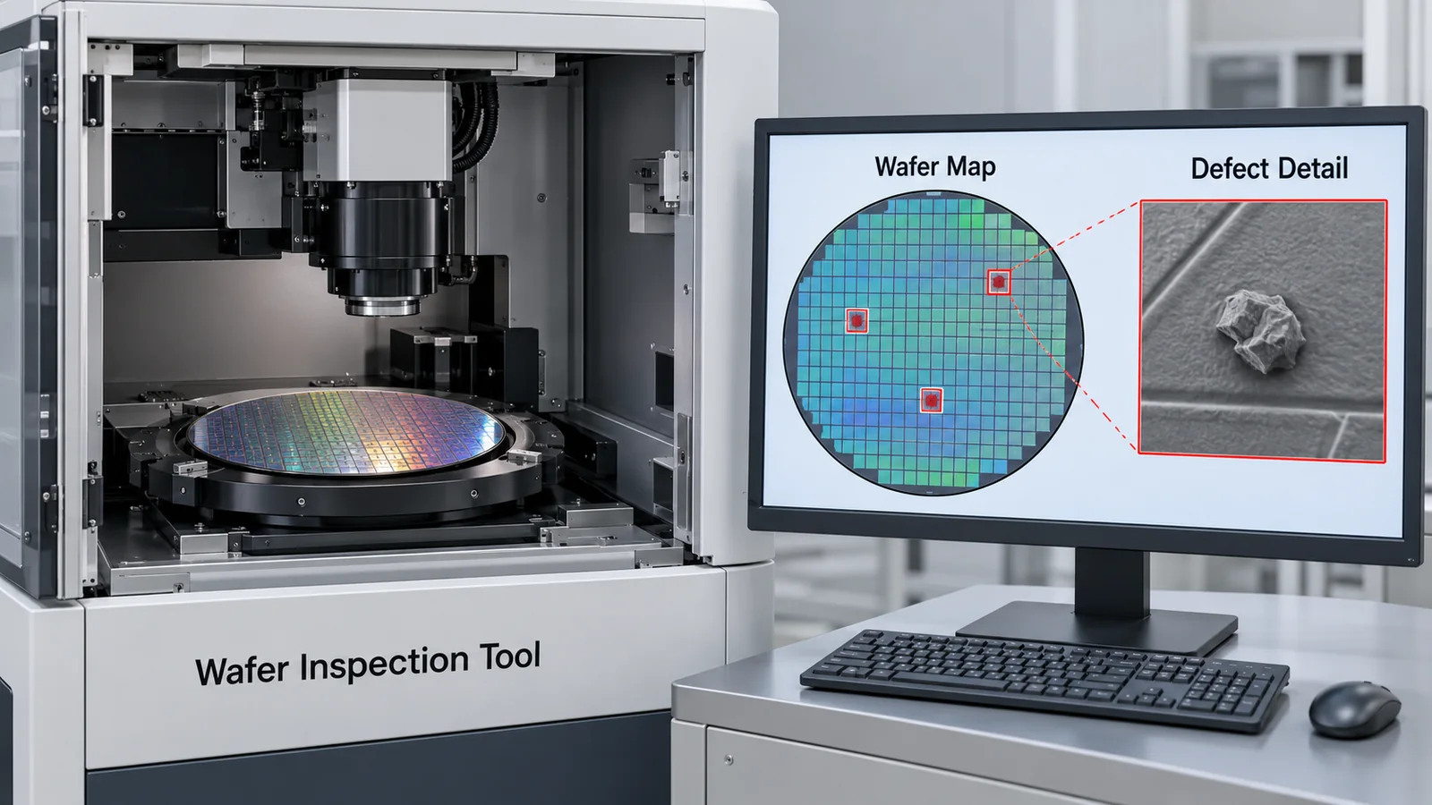
- Manufacturing: defect inspection and yield analysis, picking yield-relevant defects out of optical "noise"
- Computational lithography and digital twins: separating production from "being explored"
- Fab data and standards: SEMI standards for communication, data collection and cybersecurity
- Our calculation: what a 5% smaller die does to yield and the number of good dies
- Limits, and what could not be confirmed
- How to read evaluations and standards
- Glossary
- References
- Claim-to-source audit
Sourced = stated in a published source (linked)
Our calculation = a value this article derives from stated assumptions
Not yet confirmed = plans, schedules or proposals not yet confirmed as results
Interpretation and organization are marked as commentary. An inference is shown in bold.
The "N-fold" and "N% reduction" figures here are values reported by companies or researchers under their own conditions and are not necessarily independently verified. Design results depend on the kind of design, step, tool version and baseline, and figures from different reports are not lined up to rank them. We distinguish production use (a company publishes use in customers' volume production or in manufacturing), reports of internal use, research and evaluation stage and concept or exploration, and the last two are not written up as results. For contested evaluations we give both sides' statements without a verdict. No companies or products are ranked.
1. AI in semiconductor design and manufacturing (the short version)
- Design: exploration and assistance. There are two lines: automating the search of placement, routing and design parameters, for example with reinforcement learning (Synopsys DSO.ai, Cadence Cerebrus, Google's AlphaChip), and assisting with design documents, scripts and log analysis with language models (NVIDIA's ChipNeMo).Sourced[Ref. 3][Ref. 6][Ref. 7][Ref. 8]
- Manufacturing: defects and data. Applied Materials has published a technique that tells yield-relevant defects from the many signals of optical inspection using a small sample of electron-beam review and AI.Sourced[Ref. 10] On 31 May 2026 NVIDIA announced that TSMC is using computational lithography (cuLitho) and other tools, and describes a fab digital twin (FabTwin) as "being explored".Sourced[Ref. 13]
- Some evaluations are split. The AlphaChip placement results coexist with a Nature paper, an ISPD 2023 paper that re-evaluated them, and rebuttals from both sides (Chapter 3).Sourced This article gives no verdict and shows each side's statements and what could not be confirmed.
"Designed with AI" and "AI raised yield" can be read only once you know which step, compared with what, and reported by whom. And yield depends on both design-side die area and manufacturing-side defect density in an exponent (our calculation in Chapter 8). Materials and process engineers hold the second lever without waiting for AI.
2. The chip design flow and where AI enters, with status labels
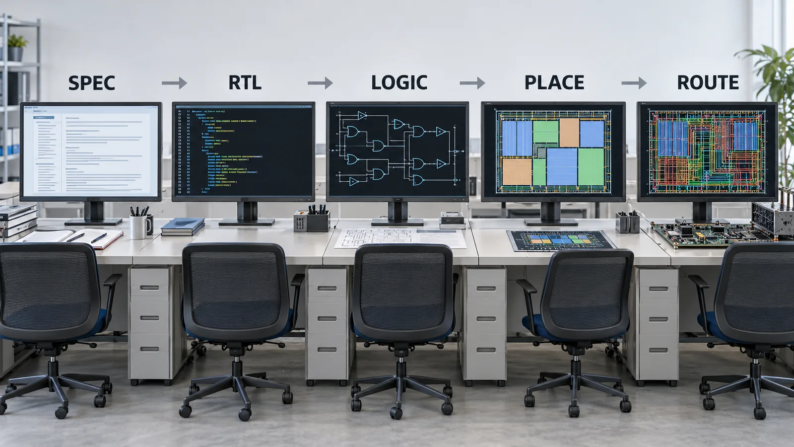
Chip design proceeds from specification through RTL (circuit description), logic synthesis, floorplanning and placement, routing, verification and signoff, to producing manufacturing data (tape-out) (our summary). The figure and table below set out where AI enters and what official material confirms. "Production use" means a company publishes use on customers' or its own real chips; "report of internal use" means a company reports internal evaluation or use; "research and evaluation" means claims still debated in papers and assessments.
View original SVG, values and source annotations
3. Placement and design-space exploration: company reports and the AlphaChip debate
Design-space exploration. On 7 February 2023 Synopsys announced that commercial tape-outs using DSO.ai (Design Space Optimization AI) reached 100 (the company's announcement). DSO.ai is described as using reinforcement learning to autonomously search a large space of solutions for good power, performance and area (PPA). The same announcement quotes customers: STMicroelectronics raising PPA-exploration productivity by more than 3x with DSO.ai on Azure, and SK hynix reducing die size by up to 5% on its most advanced process technologies.Sourced[Ref. 6] In a 9 June 2022 announcement Cadence said MediaTek and Renesas had adopted Cerebrus, a reinforcement-learning engine, in production flows; MediaTek cited a 5% die-area reduction and more than 6% power reduction on an SoC block and Renesas a 75% improvement in total negative slack (TNS) on an advanced-node CPU design (both customer quotes).Sourced[Ref. 7]
These are company announcements and customer quotes; the baseline (a human design or an earlier tool version), the block, the process and the measurement differ between announcements. This article does not line up the factors and percentages to rank them.
Reinforcement learning for placement, and the debate over its evaluation. Google's Mirhoseini et al. treated chip placement as a reinforcement-learning problem and reported that "in under 6 hours" the method can generate placements that are "superhuman or comparable" on modern accelerator netlists, whereas existing baselines "require human experts in the loop and take several weeks" (a 2020 preprint, published in Nature in 2021).Sourced[Ref. 1] A Nature addendum of 26 September 2024 and Google DeepMind's official blog call the method AlphaChip and, alongside a released pre-trained checkpoint, describe its use across several TPU generations, Axion processors and at MediaTek (the company's account; the blog contains no independent critique).Sourced[Ref. 2][Ref. 3]
| Issue | Statement from the Google side | Statement from the re-assessing side |
|---|---|---|
| Status of the evaluation | A peer-reviewed Nature paper; says the ISPD 2023 paper was a non-peer-reviewed invited paper that did not run the method as described in Nature [5] | Cheng et al. say they provide an improved assessment of Google Brain's reinforcement-learning macro placement and the updated Circuit Training implementation and release public benchmarks, evaluation flows and scripts [4] |
| Specific disagreements | Says the other work did not pre-train, used fewer resources (20x fewer RL experience collectors, half the GPUs), did not train to convergence and used unrepresentative test cases [5] | Uses a stronger simulated-annealing baseline and a commercial place-and-route tool for post-route power, performance and area as a "true reward"; offers insights on reproducibility and reporting and says confirmation of scalability and the pre-training method is "still missing" [4] |
| How this article treats it | Recorded as a production report (the company's account) | Recorded as part of the debate. This article adopts neither conclusion |
All Sourced (a summary of what each document's authors state; this article does not judge which side is right). The ISPD 2023 paper is bibliographically "Assessment of Reinforcement Learning for Macro Placement", DOI 10.1145/3569052.3578926, and the updated version is arXiv 2302.11014 [4].
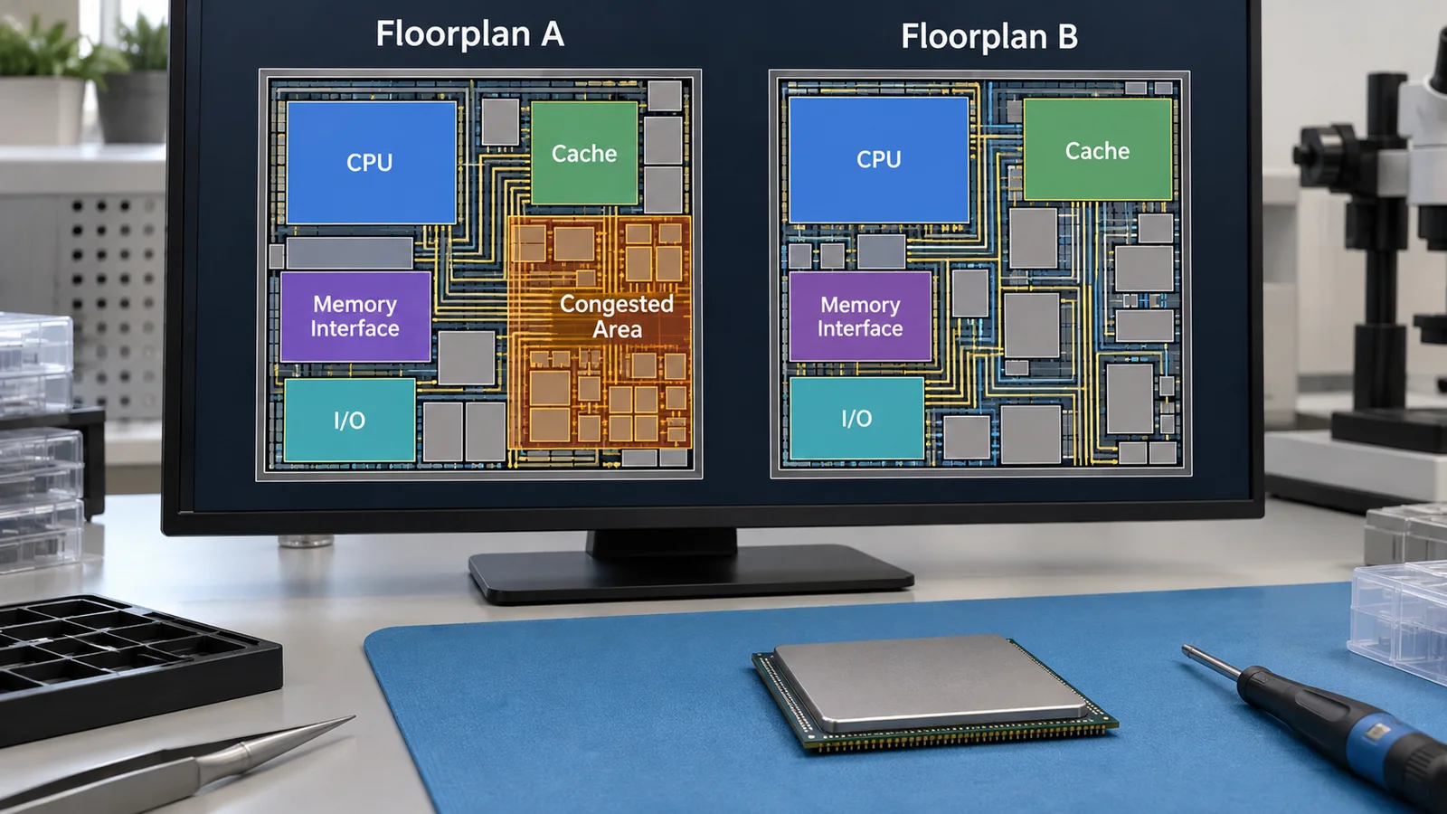
Optimizing placement and routing looks numerically like a search of power, performance and area, but behind it are materials and process quantities: wire resistance and capacitance, layer thickness, delay and heat. That a commercial place-and-route tool is used as the "true reward" in the evaluation (Cheng et al.)Sourced[Ref. 4] means design AI is ultimately judged by process models (delay and power libraries). If the process model drifts from the real silicon, the optimization drifts with it (our commentary).
In that sense, the measurements that materials and process engineers hold (wire resistance, dielectric constants, film-thickness distributions) set the quality of the inputs to design AI. As AI speeds up the search on the design side, the accuracy of process characterization may become the bottleneck, which is this article's inference (no source).
4. Language-model assistance for design: ChipNeMo and the yardsticks used
NVIDIA's ChipNeMo, instead of using off-the-shelf commercial or open models as they are, domain-adapts a language model to chip design (domain-adaptive tokenization, continued pre-training, instruction alignment and retrieval-model adaptation). Its three evaluated uses are an engineering-assistant chatbot, EDA script generation, and bug summarization and analysis, and the authors report that the largest model, ChipNeMo-70B, outperformed GPT-4 on two of them and was competitive on the third (NVIDIA's own evaluation for its own use cases).Sourced[Ref. 8] This is a report of internal use; third-party reproduction and figures for production-chip outcomes could not be found.
As a public yardstick, VerilogEval is a framework for evaluating Verilog (a hardware description language) code generation, consisting of 156 problems from the Verilog instructional site HDLBits, in which generated code is checked automatically for functional correctness by comparing simulation output with a golden solution.Sourced[Ref. 9] It centers on small circuit tasks and does not show the quality of real designs of millions of gates (our caution).
RTL and scripts written by a language model need to be checked by simulation, formal verification and signoff just like human-written ones. VerilogEval being built to check functional correctness by simulationSourced[Ref. 9] reflects that thinking. Raising generation quality and being able to skip verification are different matters, and no official material showing the latter was found in this article's research.
5. Manufacturing: defect inspection and yield analysis, picking yield-relevant defects out of optical "noise"
In an announcement of 16 March 2021 Applied Materials presented the use of big data and AI in process control. The challenge is telling yield-relevant defects from "noise" (harmless signals) among the many signals produced by an optical wafer inspection tool (Enlight). ExtractAI connects, in real time, the large volume of optical inspection data with an electron-beam tool (SEMVision) that reviews and classifies individual defects, and Applied says it can classify all candidate defects on the wafer map after reviewing only 0.001X of the samples. It adds that the AI adapts to new defects during volume production and improves as more wafers are scanned (the company's claim; no independent verification was found).Sourced[Ref. 10]
Classifying wafer maps for yield analysis is also widely studied. The paper by Wu et al. in IEEE Transactions on Semiconductor Manufacturing (2015) deals with recognizing failure patterns and similarity search for large-scale wafer-map data, and the data used there, called WM-811K, has been used as a standard in many later studies (per later studies; the original text was not read).Sourced[Ref. 11] Public data, however, comes from one manufacturing environment at one time, so whether it applies to your own process needs separate confirmation (our caution).
ExtractAI's idea is to correct a large volume of signals with a small number of reliable observations, but Applied's own announcement describes the challenge as small variations from 3D transistor formation and multiple process steps that become yield-killing defects and take time to root-cause.Sourced[Ref. 10] Better classification accuracy does not improve yield unless it is known which film, clean or etch, under which conditions, produced the defect. Wafer-map patterns (clustering at the center, at the edge, in lines) are clues for narrowing materials and process causes (our commentary).
The other is data quality and reproducibility. Tool-to-tool variation, material lots and calibration drift change a classifier's performance. High accuracy on public data does not guarantee the same accuracy in your process. Evaluation should use your own data under the conditions of the tools actually used (our commentary).
6. Computational lithography and digital twins: separating production from "being explored"
Computing the correction of mask patterns so they print the intended shapes on the wafer (computational lithography) needs enormous computation. In an announcement of 18 March 2024 NVIDIA said cuLitho speeds this computation up by 40 to 60 times (in joint tests 45x for curvilinear flows and nearly 60x for traditional Manhattan flows), that 350 H100 systems can replace 40,000 CPU systems, and that TSMC CEO C.C. Wei said "We are moving NVIDIA cuLitho into production at TSMC" (NVIDIA's announcement and an executive's quoted statement).Sourced[Ref. 12]
NVIDIA's announcement of 31 May 2026 (GTC Taipei) says TSMC is using cuLitho, that cuLitho improves cost effectiveness or cycle time by 20% to 50% compared with CPU-based computational lithography (with no stated basis for the range), that cuEST (chemistry simulation) is on average 50x faster for semiconductor material design, and that cuML is used for process control, Metropolis and the TAO Toolkit for inspection, and H200 for fab scheduling. On the other hand it describes a virtual fab environment, "FabTwin" (a digital twin using Omniverse libraries), as being explored (NVIDIA's announcement; no independent verification was found).Sourced[Ref. 13] The 2024 "40 to 60 times" and the 2026 "20% to 50%" differ in what is compared and in the metric, and are not updates of one number.
On terminology and framework for digital twins, the international standard ISO 23247-1:2021, "Automation systems and integration — Digital twin framework for manufacturing — Part 1: Overview and general principles", provides an overview and general principles of a digital-twin framework for manufacturing, including terms and definitions and requirements (title, edition and status confirmed on the ISO page; text not read).Sourced[Ref. 15] Lithography itself (EUV, masks, resists) is covered in our explainer on lithography and EUV, and etching in our explainer on etching.
| Item | What official material states | Status |
|---|---|---|
| cuLitho (computational lithography) | NVIDIA writes that TSMC's CEO said it is moving into production (2024), and that TSMC is using it in 2026 [12, 13] | Production use (company report) |
| cuML, Metropolis, TAO and H200 (fab process control, inspection and scheduling) | Stated as in use, but described qualitatively with no figures [13] | Production use (company report, no figures) |
| cuEST (chemistry simulation for semiconductor materials) | States "50x faster on average"; basis not given [13] | Company claim |
| FabTwin (a fab digital twin) | States TSMC is "exploring" building it with Omniverse libraries [13] | Not yet confirmed concept or exploration |
Column 2 summarizes NVIDIA's announcements (18 March 2024 and 31 May 2026); no independent verification was found. TSMC's own official announcements were not checked for this article.
7. Fab data and standards: SEMI standards for communication, data collection and cybersecurity
SEMI's smart manufacturing page says modern fabs gather constant streams of data from hundreds of sensors and use them to improve yield, mitigate defects and enhance productivity, and lists the standards underpinning this.Sourced[Ref. 14] The data flow that AI consumes rests on standards for equipment communication (SECS-I, SECS-II, HSMS and GEM), equipment data acquisition (EDA, Interface A), process control, data quality and cybersecurity. The list as checked on 15 October 2026 shows the following editions.Sourced[Ref. 14]
| Area | SEMI standard (number, edition, title) | Relation to AI and data use (our summary) |
|---|---|---|
| Equipment communication and control | E5-0622 (SECS-II message content), E30-0423 (GEM), E37-0222 (HSMS) | The long-standing basic communication for taking data from and sending recipes to tools |
| Equipment data acquisition (EDA) | E120-0922 (Common Equipment Model), E125-1022 (Equipment Self Description), E134-1022 (Data Collection Management), E164-0414 (EDA Common Metadata), E132-0922 (client authentication), E178-0120 (EDA Freeze Version guide), E179-0822 (Protocol Buffers common components) | A framework for collecting many sensor streams at high speed; the source of inputs for AI training and inference |
| Predictive analytics and process control | E116-0518 (Equipment Performance Tracking), E126-0708 (Equipment Quality Information Parameters), E133-1218 (Automated Process Control Systems Interface), E157-0611 (Module Process Tracking) | The framework linking inputs and outputs of virtual metrology and process control |
| Data quality | E151-1211 (Guide for Understanding Data Quality), E160-1211 (Specification for Communication of Data Quality) | A mechanism for conveying the quality of the data that enters AI |
| Cybersecurity | E187-0122 (Cybersecurity of Fab Equipment), E188-0222 (Malware-Free Equipment Integration) | Connecting data to AI platforms widens the attack surface, so requirements are set on the equipment side |
Column 2 is as listed on SEMI's standards page (number, edition, title). Column 3 is our summary; the standards' texts are paid and were not read, and no requirements are inferred.
8. Our calculation: what a 5% smaller die does to yield and the number of good dies
As results of design AI, Synopsys's announcement quotes SK hynix reducing die size "by up to 5%" and Cadence's announcement quotes MediaTek's "5% die-area reduction", both as customer quotes.Sourced[Ref. 6][Ref. 7] A smaller die (1) lets more dies fit on one wafer and (2) lowers the chance that a defect lands in a given die, raising yield. A simple model gives the size of the effect.
Our calculation Model: 300 mm wafer; gross dies ≈ π(d/2)² / A − πd / √(2A) (d = 300 mm, A = die area; a common approximation that subtracts edge losses). Yield Y = exp(−A x D0) (a Poisson model; A in cm², D0 is defect density in defects/cm²).
Die area: from 100 mm² (10 mm square) to 95 mm², 5% less. Gross dies go from about 640 to about 676 (+5.5%).
Yield and good dies (by defect density D0): at D0 = 0.10/cm², Y goes 90.5% → 90.9% and good dies 579 → 614 (+6.1%). At D0 = 0.50/cm², Y goes 60.7% → 62.2% and good dies 388 → 420 (+8.2%).
The other lever: for the same 100 mm² die, lowering D0 from 0.5 to 0.1 defects/cm² raises Y from 60.7% to 90.5% (about 1.49x), a larger effect than the 5% die shrink (about +6% to +8% in good dies).
Assumptions and limits: D0 (0.05 to 0.5 defects/cm²) is entirely assumed and is not the defect density of any process or product. The Poisson model simplifies by assuming defects are independent and uniformly scattered; real defects tend to cluster, and yield is generally said to come out higher than this, but we make no such correction (general knowledge not sourced here). Redundancy repair, parametric yield loss, edge exclusion and scribe-line width are excluded. A 5% shrink is not obtained without other performance or cost trade-offs.
In Y = exp(−A x D0), even if design AI shrinks A by 5%, yield stays low if D0 is large. The lever that lowers D0 (material purity, film uniformity, clean and polish conditions, tool cleanliness) belongs to materials and process engineers, and multiplies with the results of design AI (commentary based on our calculation). AI enters here too, as defect classification (Chapter 5), by speeding the work of lowering D0.
How demand for AI chips (GPUs and HBM) is pushing larger dies and advanced packaging is covered in our explainers on AI accelerators, HBM and CoWoS. The larger the die, the more the A x D0 exponent bites, so defect-density control matters more (our commentary).
9. Limits, and what could not be confirmed
- Independent verification: the figures from Synopsys, Cadence, Applied Materials and NVIDIA (3x, 5%, 0.001X, 40 to 60x, 20% to 50% and so on) are company announcements and customer or executive quotes; no independent verification was found. TSMC's own official announcements were not checked.
- The AlphaChip evaluation: the Nature paper, the addendum, the ISPD 2023 assessment and rebuttals from both sides coexist, and this article reaches no verdict. The Nature text was not read; what was read are the preprint abstract, the addendum's bibliographic record, the DeepMind blog, the ISPD abstract and the rebuttal abstract.
- Extent of production use: official material did not show which chips and which designs used AI tools or what share they account for. The tape-out count (Synopsys's 100 in February 2023) is a 2023 figure and a current count was not found.
- Texts of standards: for the SEMI standards, ISO 23247-1, ISO/IEC TS 4213:2022 and others only numbers, titles and editions (or status) were confirmed; the texts are paid and not read, and no requirements are inferred.
- Areas not covered: AI use in lithography (EUV), etching, deposition, cleaning and CMP and back-end packaging is covered in other explainers in this series. AI for analog and RF design, DFT and test, and formal verification in EDA is not treated in depth.
- Read production use, internal use, research and exploration apart. Design-space exploration is reported as production use by companies with customer quotes, ChipNeMo is a report of internal use and FabTwin is under exploration.Sourced
- The AlphaChip evaluation remains debated, and this article gives no verdict. Both sides' statements and what could not be confirmed are shown.Sourced
- In manufacturing, defect classification and data standards are the foundation. Applied links optical inspection and electron-beam review with AI, and SEMI's EDA standards and others underpin fab data.Sourced
- Yield depends on both area and defect density in the exponent. In our calculation a 5% die shrink gave about +6% to +8% in good dies, and lowering D0 from 0.5 to 0.1 defects/cm² gave a larger effect.Our calculation
- On evaluation and standards, SEMI standards cover communication, data and cybersecurity and ISO 23247 the digital-twin framework, but no international standard deciding pass or fail on AI results themselves was found.Sourced
10. How to read evaluations and standards
Design AI is evaluated on (1) PPA (power, performance, area) and time to tape-out, (2) the baseline (a human design, an earlier tool version or another algorithm) and (3) reproducibility (whether another party can reproduce it under the same conditions); manufacturing AI is evaluated on (1) detection and classification accuracy (misses and false alarms), (2) the effect on yield and cycle time and (3) data quality and standards. No industry-wide agreed "AI design benchmark" was found, so one reads companies' self-reports, research assessments using public data, and standards together.
| Item | Representative method or material (name, source) | Standards and guidance | How to read it |
|---|---|---|---|
| Design optimization results (PPA) | Company announcements (Synopsys, 7 February 2023; Cadence, 9 June 2022) [6, 7]. In research, the Nature paper [1], the ISPD 2023 re-assessment [4] and public benchmarks (the MacroPlacement repository) [4] Sourced | None found (an international standard to judge AI design results) | Check the baseline, block, process and tool version. Reproduction conditions (pre-training, compute, convergence) can swing the evaluation [4, 5] |
| Language-model design assistance | ChipNeMo (NVIDIA's own evaluation) [8] and VerilogEval (156 HDLBits problems, automatic functional-correctness check) [9] Sourced | ISO/IEC TS 4213:2022 (assessment of machine learning classification performance) and ISO/IEC TS 25058:2024 (guidance for quality evaluation of AI systems). Titles and status only [16] Sourced | Accuracy on small tasks is not the quality of real designs. Verify generated output before use |
| Defect inspection and yield analysis | Applied Materials ExtractAI (0.001X of samples; company claim) [10] and public wafer-map data (WM-811K, Wu et al.) [11] Sourced | ISO/IEC TS 4213:2022 (classification performance), the ISO/IEC 5259 series (data quality), and SEMI E151 and E160 (data quality) [14, 16] Sourced | Both misses and false alarms; re-evaluate on your own data and tools. Public data comes from one environment |
| Fab data, communication and security | None found (conformity of individual fabs) | SEMI E5-0622, E30-0423, E120-0922, E125-1022, E134-1022, E164-0414, E133-1218, E151-1211, E160-1211, E187-0122 and E188-0222 (numbers, editions and titles confirmed on SEMI's page) [14] Sourced | The standards set communication and data conventions and do not decide AI performance. The texts are paid and not read |
| Digital twins | FabTwin (NVIDIA and TSMC's exploratory effort) [13] Not yet confirmed | ISO 23247-1:2021 (digital twin framework for manufacturing: overview and general principles) [15] Sourced | The term "digital twin" is used broadly; tell production from exploration by the wording in official material (exploring or in use) |
| Acceleration of computational lithography | NVIDIA announcements (18 March 2024: 40 to 60x; 31 May 2026: 20% to 50%) [12, 13] Sourced (company claims) | None found | Figures with different baselines and metrics are different things. No independent verification found |
Category tags appear in each cell. The SEMI and ISO pages were checked in a browser on 15 October 2026. The arrangement of the table is our own.
Three points on how to read these.
- Who reports it: company announcements and customer or executive quotes are not independent verification. For results under debate (AlphaChip), read both sides and check the reproduction conditions (pre-training, compute, convergence).
- What it is compared with: factors with different baselines (a human design, an earlier tool, another algorithm, CPU computation) are different numbers. As with "40 to 60x" in 2024 and "20% to 50%" in 2026, different metrics are not updates.
- Standards mostly cover data and communication: SEMI standards address tool and factory data, communication and security, and ISO 23247 the digital-twin framework; they do not decide pass or fail on AI results. Whether a standard is a requirement or a recommendation must be checked in its text, which this article did not read.
11. Glossary
- EDA
- Electronic design automation: software for chip design.
- PPA
- Power, performance, area.
- RTL
- Register-transfer level: the design level that describes circuit behaviour.
- Placement (floorplan)
- The step that decides where circuit blocks sit on the chip.
- Tape-out
- Completing and releasing the design data for manufacturing.
- Yield
- The share of good dies among those made.
- Defect density D0
- Number of killer defects per unit area.
- Computational lithography
- Correcting mask patterns by computation so they print as intended on the wafer.
- Digital twin
- A model that mirrors a real fab or tool in virtual space.
- SECS / GEM / EDA
- SEMI standards for equipment communication and data acquisition.
- PoC
- Proof of concept: a demonstration stage, distinct from volume or production use.
- Virtual metrology
- Predicting unmeasured quality from tool data.
12. References
- Mirhoseini A. et al. (Google) "A graph placement methodology for fast chip design", Nature (2021), DOI 10.1038/s41586-021-03544-w. Preprint "Chip Placement with Deep Reinforcement Learning", arXiv 2004.10746 (the "under 6 hours" and "superhuman or comparable" statement) — arxiv.org/abs/2004.10746
- Nature "Addendum: A graph placement methodology for fast chip design", Nature (26 September 2024), DOI 10.1038/s41586-024-08032-5 (bibliographic record only) — doi.org/10.1038/s41586-024-08032-5
- Goldie A., Mirhoseini A. (Google DeepMind) "How AlphaChip transformed computer chip design", Google DeepMind blog (26 September 2024) (several TPU generations, Axion, MediaTek, release of a pre-trained checkpoint) — deepmind.google/blog/how-alphachip-transformed-computer-c...
- Cheng C.-K. et al. "Assessment of Reinforcement Learning for Macro Placement", ISPD 2023, DOI 10.1145/3569052.3578926. Updated version "An Updated Assessment of Reinforcement Learning for Macro Placement", arXiv 2302.11014 — arxiv.org/abs/2302.11014
- Goldie A. et al. "That Chip Has Sailed: A Critique of Unfounded Skepticism Around AI for Chip Design", arXiv 2411.10053 (2024) — arxiv.org/abs/2411.10053
- Synopsys "AI-designed Chips Reach Scale with First 100 Commercial Tape-outs Using Synopsys Technology" (7 February 2023; DSO.ai, quotes from STMicroelectronics and SK hynix) — news.synopsys.com/2023-02-07-AI-designed-Chips-Reach-Scal...
- Cadence "Cadence Cerebrus AI-Based Solution Delivers Transformative Results on Next-Generation Customer Designs" (9 June 2022; quotes from MediaTek and Renesas) — cadence.com/en_US/home/company/newsroom/press-releases/pr...
- Liu M. et al. (NVIDIA) "ChipNeMo: Domain-Adapted LLMs for Chip Design", arXiv 2311.00176 (2023) — arxiv.org/abs/2311.00176
- Liu M. et al. (NVIDIA) "VerilogEval: Evaluating Large Language Models for Verilog Code Generation", arXiv 2309.07544 (2023) — arxiv.org/abs/2309.07544
- Applied Materials "Applied Materials Introduces New Playbook for Process Control Based on Big Data and AI" (16 March 2021; Enlight, ExtractAI and SEMVision) — ir.appliedmaterials.com/news-releases/news-release-detail...
- Wu M.-J. et al. "Wafer Map Failure Pattern Recognition and Similarity Ranking for Large-Scale Data Sets", IEEE Trans. Semiconductor Manufacturing 28(1) (2015), DOI 10.1109/TSM.2014.2364237 (bibliographic record confirmed on Crossref; text not read) — doi.org/10.1109/TSM.2014.2364237
- NVIDIA "NVIDIA cuLitho Accelerates Semiconductor Manufacturing's Most Compute-Intensive Workload by 40-60x" / "TSMC and Synopsys Bring Breakthrough NVIDIA Computational Lithography Platform to Production" (18 March 2024) — nvidianews.nvidia.com/news/tsmc-synopsys-nvidia-culitho
- NVIDIA "NVIDIA and TSMC Bring AI Into Fabs to Advance Semiconductor Design and Manufacturing" (31 May 2026, GTC Taipei; cuLitho 20% to 50%, cuEST, FabTwin being explored) — nvidianews.nvidia.com/news/nvidia-and-tsmc-bring-ai-into-...
- SEMI "SEMI Smart Manufacturing Standards" (list of numbers, editions and titles of standards for SECS/GEM, EDA, data quality, cybersecurity and more; checked 15 October 2026) — semi.org/en/industry-groups/smart-manufacturing/standards
- ISO "ISO 23247-1:2021 Automation systems and integration — Digital twin framework for manufacturing — Part 1: Overview and general principles" (edition 1, October 2021; ISO/TC 184/SC 4) — iso.org/standard/75066.html
- ISO/IEC JTC 1/SC 42 List of standards of SC 42 "Artificial intelligence" (ISO/IEC TS 4213:2022, TS 25058:2024, the 5259 series and others; checked 15 October 2026) — iso.org/committee/6794475/x/catalogue/p/1/u/0/w/0/d/0
13. Claim-to-source audit
| Claim in the text | Basis | Category |
|---|---|---|
| Treating chip placement with reinforcement learning, "under 6 hours" with "superhuman or comparable" placements, existing baselines taking weeks with humans in the loop (preprint abstract) | Reference 1 https://arxiv.org/abs/2004.10746 | Sourced |
| Bibliographic record of the Nature addendum (26 September 2024) | Reference 2 https://doi.org/10.1038/s41586-024-08032-5 | Sourced |
| Google DeepMind blog: the AlphaChip name, several TPU generations (v5e, v5p, Trillium), Axion, MediaTek, release of a pre-trained checkpoint, the time claim; no independent critique included | Reference 3 https://deepmind.google/blog/how-alphachip-transformed-computer-chip-design/ | Sourced |
| The ISPD 2023 re-assessment (a stronger simulated-annealing baseline, post-route PPA from a commercial tool, public benchmarks, reproducibility, and "still-missing" confirmations on scalability and pre-training) | Reference 4 https://arxiv.org/abs/2302.11014 | Sourced |
| The Google-side rebuttal (no pre-training, fewer resources, no training to convergence, unrepresentative test cases, and its description of a non-peer-reviewed invited paper) | The authors' statements; this article does not judge which is right Reference 5 https://arxiv.org/abs/2411.10053 | Sourced |
| Synopsys: 100 commercial tape-outs with DSO.ai (7 February 2023), reinforcement-learning search, STMicroelectronics' more-than-3x PPA-exploration productivity, SK hynix's die-size reduction of up to 5% | Reference 6 https://news.synopsys.com/2023-02-07-AI-designed-Chips-Reach-Scale-with-First-100-Commercial-Tape-outs-Using-Synopsys-Technology | Sourced |
| Cadence: Cerebrus (reinforcement learning), MediaTek's 5% die-area reduction and more-than-6% power reduction, Renesas' 75% TNS improvement (9 June 2022), and adoption in production flows | Reference 7 https://www.cadence.com/en_US/home/company/newsroom/press-releases/pr/2022/cadence-cerebrus-ai-based-solution-delivers-transformative.html | Sourced |
| ChipNeMo: domain-adaptation methods, three use cases, ChipNeMo-70B outperforming GPT-4 on two (NVIDIA's own evaluation) | Reference 8 https://arxiv.org/abs/2311.00176 | Sourced |
| VerilogEval: 156 HDLBits problems, automatic functional-correctness check by simulation | Reference 9 https://arxiv.org/abs/2309.07544 | Sourced |
| Applied Materials: ExtractAI, linking optical inspection and electron-beam review, classification after 0.001X of samples, adaptation during volume production (16 March 2021; company claim) | Reference 10 https://ir.appliedmaterials.com/news-releases/news-release-details/applied-materials-introduces-new-playbook-process-control-based/ | Sourced |
| Bibliographic record of the paper by Wu et al. (IEEE TSM 28(1), 2015, DOI) and its subject of wafer-map failure-pattern recognition and similarity ranking | Reference 11 https://doi.org/10.1109/TSM.2014.2364237 | Sourced |
| NVIDIA (18 March 2024): cuLitho 40 to 60x (45x for curvilinear and nearly 60x for Manhattan flows), 350 H100 systems replacing 40,000 CPU systems, the TSMC CEO's "moving into production" statement | Reference 12 https://nvidianews.nvidia.com/news/tsmc-synopsys-nvidia-culitho | Sourced |
| NVIDIA (31 May 2026): TSMC using cuLitho, a 20% to 50% improvement, cuEST 50x on average, use of cuML, Metropolis, TAO and H200, and FabTwin being explored | Reference 13 https://nvidianews.nvidia.com/news/nvidia-and-tsmc-bring-ai-into-fabs-to-advance-semiconductor-design-and-manufacturing | Sourced |
| FabTwin is "being explored", not production use | Reference 13 https://nvidianews.nvidia.com/news/nvidia-and-tsmc-bring-ai-into-fabs-to-advance-semiconductor-design-and-manufacturing | Not yet confirmed |
| SEMI standard numbers, editions and titles (E5-0622, E30-0423, E37-0222, E116-0518, E120-0922, E125-1022, E126-0708, E132-0922, E133-1218, E134-1022, E151-1211, E157-0611, E160-1211, E164-0414, E178-0120, E179-0822, E187-0122, E188-0222) and the statement that modern fabs gather data from hundreds of sensors | Reference 14 https://www.semi.org/en/industry-groups/smart-manufacturing/standards | Sourced |
| The title, edition and status of ISO 23247-1:2021 and its overview and general principles (terms, definitions and requirements) | Reference 15 https://www.iso.org/standard/75066.html | Sourced |
| Titles, editions and statuses of ISO/IEC TS 4213:2022, TS 25058:2024 and the 5259 series | Reference 16 https://www.iso.org/committee/6794475/x/catalogue/p/1/u/0/w/0/d/0 | Sourced |
| Gross dies on a 300 mm wafer (about 640 at 100 mm², about 676 at 95 mm²), Poisson-model yield and good dies (D0 = 0.05, 0.1, 0.3, 0.5 defects/cm²), and the effect of lowering D0 from 0.5 to 0.1 | Our calculation. D0 is assumed and the Poisson model is a simplification (it excludes defect clustering and redundancy repair). Not a prediction for any process or product | Our calculation |
| The readings "design AI is a tool for searching the physics of wiring and layers", "classification becomes yield only when tied to a materials cause" and "area in the yield exponent is design while defect density is materials and process"; the view that process characterization accuracy may become the bottleneck (inference) | This article's organization and commentary based on published material, not views stated by the companies | Commentary |
| Independent verification of company figures, a verdict on the AlphaChip evaluation, the extent of production use, texts of standards, and TSMC's own official announcements | Not confirmed within this article's research and therefore not given; this article's note | Commentary |
Last updated: 15 October 2026. Sources are limited to primary material (Nature bibliographic records, official announcements from Google DeepMind, Synopsys, Cadence, Applied Materials and NVIDIA, papers, and SEMI and ISO official pages). Independent verification of company figures, a verdict on the AlphaChip evaluation, the extent of production use and the texts of standards could not be confirmed and are not given. Companies' concepts and exploratory efforts are "not yet confirmed". Figures 2 and 5 are vector drawings, Figure 4 includes our calculation, and Figures 1 and 6 are AI-image placeholders only.