TECHNOLOGY EXPLAINER
Graphene and Carbon Nanotubes
— the difficulty of using “one atom of carbon” as an electrode and a transistor
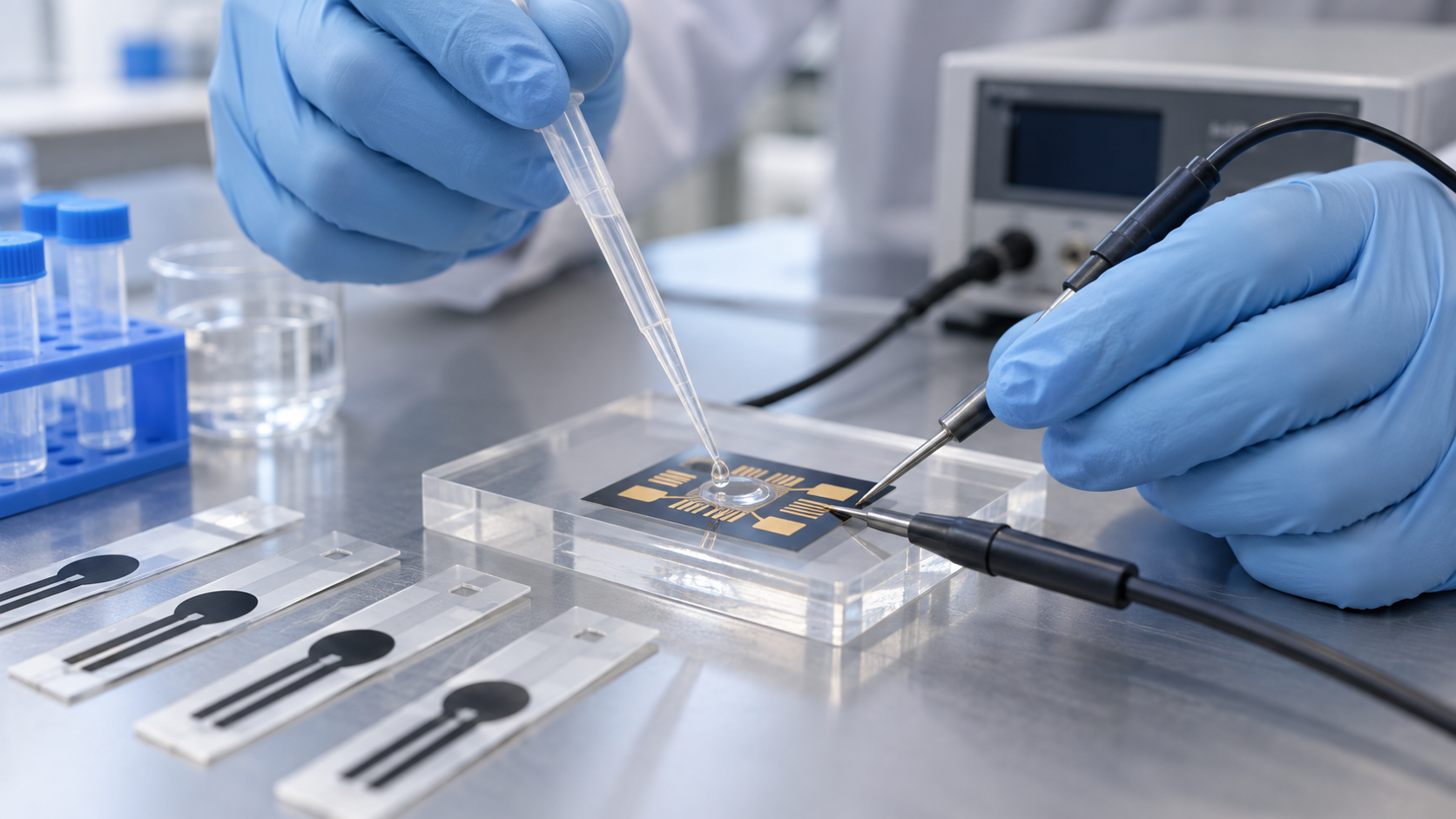
Graphene is a one-atom-thick sheet of carbon atoms arranged in hexagons; a carbon nanotube (CNT) is that sheet rolled into a tube. They conduct electricity well and every atom is exposed at the surface, so they are studied as materials for biosensor electrodes and as the channel of a field-effect transistor (FET) that turns a change of surface charge into a change of current. Electrode and sensor-chip products using them are already on sale. What interests a materials engineer is that, under the same names “graphene” and “CNT”, the performance changes greatly with how the material is made, how it is moved, and how its surface is contaminated or treated. This article covers properties, the two ways graphene and CNTs are used in biosensors, manufacturing (exfoliation, CVD, printing), functionalization, reproducibility, uniformity and cost, and biocompatibility and regulatory position, based on papers, manufacturer documents, standards and regulators' documents.
- What graphene and CNTs are, in three lines
- Properties: an atomic sheet and a rolled tube
- Two ways to use them in biosensors: electrode and FET
- Manufacturing: exfoliation, CVD and printing
- A materials engineer's view 1: transfer residues and the firing temperature of printed ink
- Functionalization: attaching recognition elements, and non-specific adsorption
- Reproducibility, uniformity and cost
- A materials engineer's view 2: what is called “graphene” is not uniform inside
- Biocompatibility, safety and regulatory position
- Examples we can confirm, and what we could not confirm
- Glossary / References / Claim-to-source audit
Sourced = stated in published material or a paper (link given)
Our calculation = a figure this article derived, with the assumptions spelled out
Not yet confirmed = at the research stage or an outlook, with no confirmed practical record
Structural readings and materials-design interpretations are marked separately as Commentary.
This article explains materials, principles and evaluation. It is not medical advice on diagnosis, treatment or how to read test results, and it does not recommend any product.
The principle of FET sensors (Debye length and so on) is covered in our explainer on field-effect transistor sensors, and electrochemical electrodes in our explainer on electrochemical sensors.
1. What graphene and CNTs are, in three lines
- Graphene: in 2004 Novoselov and co-workers described carbon films a few atoms thick. The films are a two-dimensional semimetal with a strong ambipolar electric field effect (electrons and holes can both be induced by a gate), with room-temperature mobilities of approximately 10,000 cm²/V·s Sourced
- CNTs: in 1991 Iijima reported “helical microtubules of graphitic carbon” Sourced. A 2006 paper says the heterogeneity of as-synthesized single-walled carbon nanotubes (SWNTs) in diameter, bandgap and electronic type precludes their widespread application in electronics, optics and sensing Sourced
- Where it is hard: a 2018 survey examined graphene from 60 producers worldwide and reported that the quality of what is sold as “graphene” is rather poor, and most of it is graphite microplatelets Sourced. The name is the same; the contents are not
“A sensor using graphene” names a material; it does not guarantee performance. The result depends on how it was made, how it was moved, what was attached and what it was exposed to. So for any paper or product, first check whether how the material was made, the number of layers, the degree of defects and the surface treatment are stated (commentary).
2. Properties: an atomic sheet and a rolled tube
Graphene is a sheet one atom thick of carbon atoms in a hexagonal (honeycomb) lattice. A CNT is this sheet rolled into a tube, either a single tube (single-walled, SWNT) or nested tubes (multi-walled, MWCNT). International terminology standards (ISO/TS 80004-3 and -13) define these terms Sourced (Chapter 9).
One way to make diameter, bandgap and electronic type (metallic or semiconducting) uniform in CNTs is density-gradient ultracentrifugation, in which surfactants change buoyant density. The 2006 paper reports isolating SWNTs in which more than 97% are within a 0.02 nm diameter range, and producing bulk quantities of SWNTs of predominantly a single electronic type, from which it made thin-film electrical devices of networked SWNTs showing either metallic or semiconducting behaviour Sourced. In other words, using SWNTs as an FET channel requires a step on the materials side to separate out the semiconducting tubes (commentary).
3. Two ways to use them in biosensors: electrode and FET
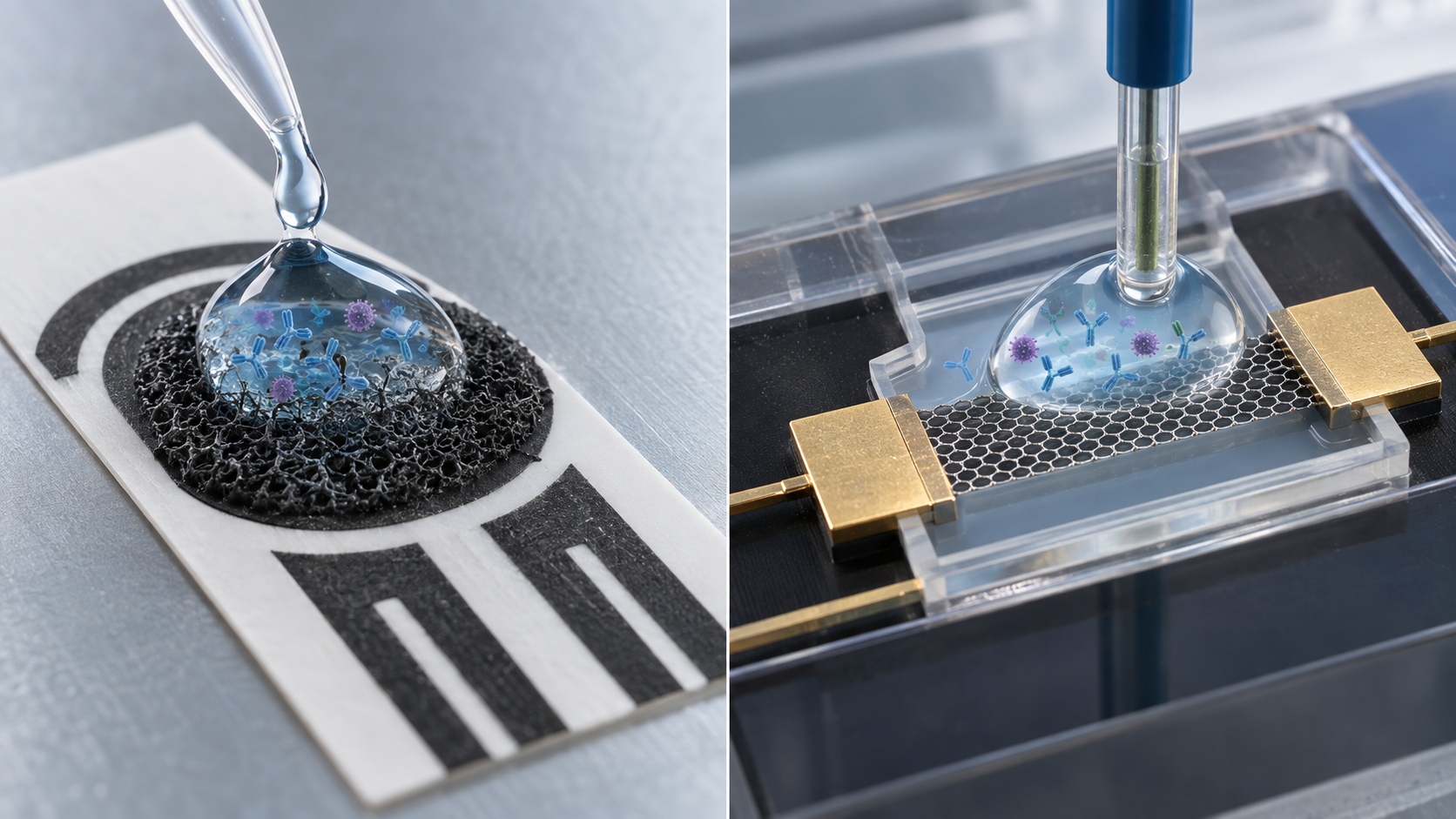
In biosensors, graphene and CNTs are used in two broad ways (our grouping).
- Electrochemical electrode: graphene or CNTs are mixed into a printed carbon electrode to raise surface area and electron transfer, and the current of an enzyme reaction or redox process is read.
- FET channel: graphene or CNTs serve as the path of current, and the charge of molecules bound to the surface changes that current, which is read.
View the original SVG schematic, source notes and numerical details
(1) Examples of electrode products
Metrohm (DropSens) lists, for biosensor development, a graphene-modified screen-printed carbon electrode (DRP-110GPH-U50) and a carboxylated multi-walled carbon nanotube-modified screen-printed carbon electrode (DRP-110CNT-U50). Both are described as designed “for the development of (bio)sensors with an enhanced electrochemical active area”, with a ceramic substrate (3.4 × 1.0 × 0.05 cm), a working electrode 4 mm in diameter with a geometric area of 0.11 cm², a carbon counter electrode and a silver reference electrode; the working-electrode material is listed as “graphene/carbon” and “MWCNT-COOH/carbon” respectively Sourced (manufacturer's stated specification). The product pages do not state the graphene or CNT content of the working electrode, the number of layers or any guaranteed performance Sourced.
(2) Examples of products and research on FET channels
Paragraf (UK) supplies graphene FET devices (PMF2000, 3 channels; PMF2002, 12 channels) “designed for sensing and research applications”. It says the graphene is grown directly without polymers, the channels are 100 × 100 µm, and an epoxy encapsulation layer allows liquid handling and channel-specific functionalisation Sourced (manufacturer's description). The specification table lists a Dirac point of 700 ± 150 mV (PMF2000), a transconductance of typical 0.8 and minimum 0.5 mS·sq/V, and a channel resistance of 1 to 3.5 kΩ, and says batch reports are available on request Sourced (manufacturer's stated values).
As a classic research example, Ohno and co-workers reported electrolyte-gated graphene FETs in 2009. Using non-functionalized single-layer graphene as the channel, they found transconductances 30 times higher in electrolyte than in vacuum, conductance increasing linearly with electrolyte pH, and conductance rising on exposure to a protein at several hundred picomolar Sourced.
In a solution containing salt, surface charge is screened by ions. Stern and co-workers reported in 2007, for nanowire FET sensors, that careful control of the solution Debye length is critical for unambiguous selective detection of macromolecules Sourced. The same applies to graphene FETs: whether measurement is possible at physiological salt concentration, or needs dilution or a low-salt buffer, bears directly on device design and sample pre-treatment (commentary; see our explainer on field-effect transistor sensors).
4. Manufacturing: exfoliation, CVD and printing
Graphene is made in three broad ways: peeling it thinly from graphite, growing carbon from the gas phase, and turning it into an ink for printing. Each has reported values and materials-side problems.
| Method | Representative report | Reported values (with conditions) | Materials-side issues (source or commentary) |
|---|---|---|---|
| Mechanical exfoliation (Scotch-tape method) | Novoselov et al. (2004) | Room-temperature mobility of about 10,000 cm²/V·s; electron and hole concentrations up to 1013 cm−2 induced by a gate Sourced | A laboratory method giving small flakes. Methods at industrial scale are being sought (statement in the review by Brownson et al.) Sourced |
| Liquid-phase exfoliation | Hernandez et al. (2008) | Graphite dispersed and exfoliated in organic solvents such as N-methyl-pyrrolidone. Concentration up to about 0.01 mg/mL, monolayer yield about 1 wt% (potentially 7–12 wt% with further processing) Sourced | Low dispersion concentration, and many thicker flakes besides monolayers. Can give conducting films and composites (same paper) |
| CVD (growth on copper foil) and transfer | Li et al. (2009), Bae et al. (2010), Suk et al. (2011) | Centimetre-scale films, predominantly single layer (few-layer regions under 5%), mobility up to 4050 cm²/V·s (Li). 30-inch films produced roll-to-roll, sheet resistance about 125 Ω/sq and transmittance 97.4% (Bae) Sourced | A transfer step from the copper to the target substrate is needed. Polymers such as PMMA are used in transfer (Suk) Sourced. Residues are discussed in Chapter 5 |
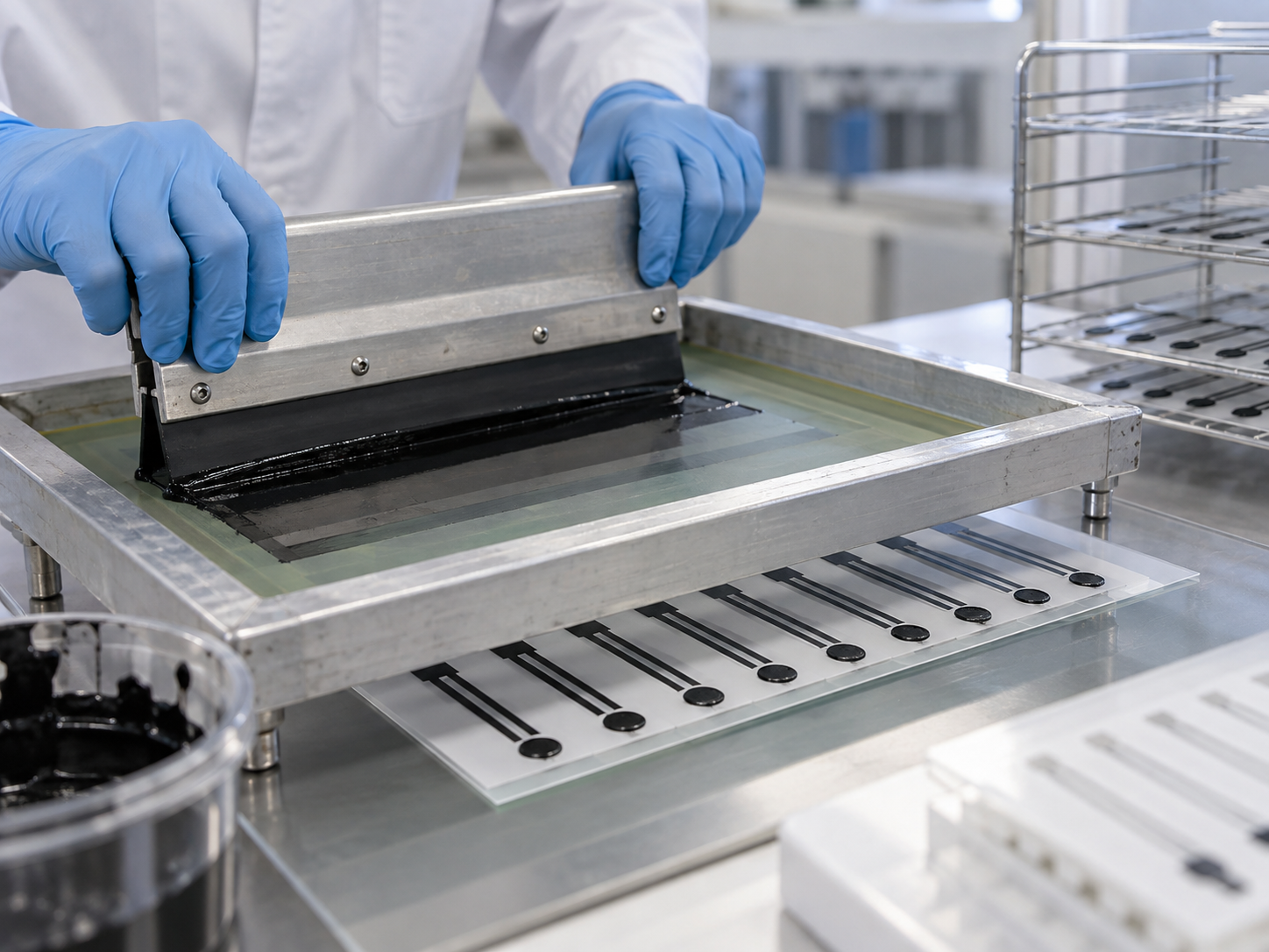
| Ink and printing | Secor et al. (2013) | Ink exfoliated and stabilized with ethanol and ethyl cellulose, inkjet printed. Resistivity of 4 mΩ·cm after a thermal anneal at 250 °C for 30 min Sourced | The stabilizing polymer has to be reduced by heat. Substrate heat resistance becomes a condition (commentary) |
Figures are those in each paper's abstract. Because substrates, doping and heat treatments differ, this table is not a ranking of the methods.
CNTs were found by Iijima in 1991 using an electron microscope Sourced and are made later by methods such as arc discharge and CVD (we did not check individual primary sources for the production methods). For biosensor use, the selection of electronic type described in Chapter 2 and removal of residual metal catalyst become materials-side work (the latter is our commentary).
We use the values from each paper for three calculations Our calculation.
- Effect of stacking (Bae): single layer, sheet resistance about 125 Ω/sq and transmittance 97.4%. Stacking four layers, the sheet resistance ideally becomes 125 / 4 = about 31 Ω/sq and transmittance 0.9744 = about 0.90 (90%). This nearly matches the paper's measured values (about 30 Ω/sq, about 90%)
- Liquid-phase exfoliation concentration (Hernandez): with a dispersion concentration up to about 0.01 mg/mL and a monolayer yield of about 1 wt%, monolayer graphene is 0.01 × 0.01 = about 0.0001 mg/mL (about 0.1 µg/mL). Reaching 1 mg/mL for the whole dispersion needs 100-fold concentration; 1 mg/mL of monolayer alone needs 10,000-fold
- Sheet resistance of a printed film (Secor): resistivity 4 mΩ·cm (= 4×10⁻³ Ω·cm). Assuming a film thickness of 1 µm, sheet resistance = resistivity / thickness = 4×10⁻³ / 1×10−4 = 40 Ω/sq. For 100 nm it would be 400 Ω/sq
Assumptions and limits: the stacking calculation is the ideal case; in practice there are interlayer contacts and transfer damage. The film thickness is our assumption. Sheet resistance of CVD films changes greatly with doping, and other values in the literature (for example about 980 Ω/sq for a monolayer on glass [Suk]) were obtained under different conditions, so they cannot be lined up to rank methods.
5. A materials engineer's view 1: transfer residues and the firing temperature of printed ink
Graphene made on copper by CVD has to be moved to another substrate to become a sensor. That transfer raises two materials problems (the following combines statements in papers and manufacturer material with our commentary).
- The polymer support film: Suk and co-workers report dry transfer in which PMMA is spin-coated over the graphene as a support and held by a PDMS frame, as well as wet transfer. A monolayer transferred onto glass had a sheet resistance of about 980 Ω/sq and a transmittance of 97.6% Sourced. That chemical residues left after transfer affect electrical properties is the subject of a paper whose title says so (Pirkle et al., 2011; by title only). Paragraf cites “polymer-free direct growth” as a reason for reproducibility Sourced (manufacturer's description)
- Interaction with the layer beneath: the surface state of the substrate and charge in the insulating layer show up in the electrical characteristics of graphene (the Dirac point). That Paragraf's device specification gives a Dirac point of 700 ± 150 mV, a range (Chapter 7), indicates that device-to-device offset of the baseline is a premise (commentary)
- Polymer in printed ink and heat treatment: the ink of Secor et al. is stabilized with ethyl cellulose and reached a resistivity of 4 mΩ·cm after 250 °C for 30 min Sourced. So the conductivity of a printed film is set by how much of the stabilizer is removed by heat. It is hard to use on substrates of low heat resistance (such as PET), and heat-resistant substrates such as polyimide (see our explainer on polyimides) become candidates (commentary)
So the “materials performance” of graphene and its “performance on a sensor” are different things, and transfer, encapsulation, substrate and thermal history are design items on the materials side (commentary).
6. Functionalization: attaching recognition elements, and non-specific adsorption
The surfaces of graphene and CNTs are bare, so a step is needed to attach recognition elements such as antibodies or aptamers. At the same time, non-specific adsorption, in which proteins you did not intend stick to the surface, has to be suppressed or the sensor does not work.
For CNTs there is a classic report that shows blocking concretely. Chen and co-workers reported in 2003 that, with single-walled CNTs, non-specific binding, found with a wide range of proteins, is overcome by immobilizing polyethylene oxide (PEO) chains. They then connected receptors specific to target proteins to the PEO-functionalized nanotubes and showed electronic sensors that detect antibodies associated with human autoimmune diseases Sourced (a research-stage report). The same group reported in 2001 non-covalent sidewall functionalization of single-walled CNTs for protein immobilization (by title) Sourced.
For graphene FETs, Seo and co-workers reported in 2020 a sensor in which an antibody against the SARS-CoV-2 spike protein was attached to a graphene FET. Reported performance: for antigen protein, 1 fg/mL in phosphate-buffered saline and 100 fg/mL in clinical transport medium; for cultured virus a limit of detection (LOD) of 1.6×101 pfu/mL; and for nasopharyngeal swabs from COVID-19 patients an LOD of 2.42×10² copies/mL. The authors state that it works without sample pretreatment or labelling Sourced. A correction (erratum) has been published for this paper Sourced. We could not confirm the content of the correction, the number of clinical samples or the sensitivity and specificity as a diagnostic, so we do not state them. This is a research report and does not show performance usable for diagnosis.
7. Reproducibility, uniformity and cost
Variability in devices and materials shows up in manufacturers' specifications. Using Paragraf's specification (PMF2000), we calculate the size of the spread Our calculation.
- Dirac point: 700 ± 150 mV. The range is 550–850 mV, 300 mV wide, or ±21% of the nominal value (150 / 700)
- Transconductance: typical 0.8, minimum 0.5 mS·sq/V. The minimum is 0.5 / 0.8 = about 63% of typical (about 37% lower)
- Channel resistance: 1–3.5 kΩ. The upper bound is 3.5 times the lower
An international standard for evaluating the material itself is ISO/TS 21356-1:2021 (structural characterization of graphene, from powders and dispersions). The standard's page says it specifies, together with the sequence of methods, sample preparation and data analysis, the characterization of the number of layers and thickness, lateral flake size, level of disorder, layer alignment and specific surface area Sourced.
On cost, we could not confirm, within the scope of this article, any primary source that gives the price or manufacturing cost of graphene FET devices or graphene-modified electrodes. Paragraf's product page has a “Buy now” link but states no price. That 30-inch films have been reported roll-to-roll (Bae) and that low cost is named as a target of printing (Secor, in the abstract) are statements that point in the direction of volume production Sourced.
8. A materials engineer's view 2: what is called “graphene” is not uniform inside
The 2018 survey by Kauling and co-workers examined graphene from 60 producers worldwide systematically by electron microscopy, atomic force microscopy, Raman spectroscopy, elemental analysis and X-ray photoelectron spectroscopy. They report that liquid-phase exfoliation has a statistical nature; that the classification of graphene flakes currently used in the market is erroneous and a new classification is needed in terms of distribution functions for the number of layers and flake size; and that most companies are producing graphite microplatelets. They suggest this poor quality may be the main reason for the slow development of graphene applications, and argue that stringent standards for graphene characterization and production, taking into account both physical properties and the requirements of the application, are the only way forward to a healthy and reliable market Sourced.
- If you buy powder or ink: rather than a data sheet that says “graphene”, check whether you can get the distribution of layers, flake size, defects and oxygen or metal impurities (commentary)
- If you buy CVD films or devices: the transfer method, whether polymer is present, the distribution of Dirac point and sheet resistance, and whether batch reports exist are the key points (matching Paragraf's statement that batch reports are available on request)
- Standards for terms: the definitions of graphene, production methods and properties are in ISO/TS 80004-13:2024 (second edition, September 2024). Part 3 of the same series (2020) covers terms for carbon nano-objects such as CNTs Sourced
9. Biocompatibility, safety and regulatory position
When graphene or CNTs are used in a sensor that touches body fluids, the safety of the material is not decided by the name of the material. A review by Fadeel and co-workers covers the synthesis and characterization of graphene-based materials (GBMs) and the human-health and environmental hazard assessment of GBMs in vitro and in vivo, and says “not all GBMs are alike, and it is essential that we disentangle the structure-activity relationships” Sourced.
(1) Carcinogenicity assessments of CNTs by an international body
The needle-like shape and length of CNTs have been associated with toxicity. Poland and co-workers reported in 2008 that long multi-walled CNTs placed in the abdominal cavity of mice (used as a surrogate for the mesothelial lining of the chest cavity) produced asbestos-like, length-dependent inflammation and granulomas; it was a pilot study, and the authors call for further research and caution Sourced. The International Agency for Research on Cancer (IARC), in Monographs Volume 111 published in 2017, evaluated CNTs as follows Sourced.
- Evidence in humans for carcinogenicity of CNTs is inadequate
- MWCNT-7 (a type of multi-walled CNT): sufficient evidence in experimental animals, and possibly carcinogenic to humans (Group 2B)
- Multi-walled CNTs other than MWCNT-7, and single-walled CNTs: inadequate evidence in animals, not classifiable as to carcinogenicity to humans (Group 3)
- The Working Group limited the scope to engineered/manufactured CNTs and did not consider CNTs specifically designed for medical purposes, for which human exposures had not yet been described
An IARC classification expresses the strength of evidence on carcinogenic hazard, not the size of risk at an actual exposure (a general reading: our commentary). The last point above matters: this monograph does not evaluate the safety of CNTs immobilized inside a biosensor.
(2) EU and US frameworks
- EU Medical Device Regulation (Regulation (EU) 2017/745): Article 2 defines “nanomaterial” and states that “fullerenes, graphene flakes and single-wall carbon nanotubes with one or more external dimensions below 1 nm shall also be deemed to be nanomaterials”. Rule 19 in Annex VIII classifies devices incorporating or consisting of nanomaterial as class III if they present a high or medium potential for internal exposure, class IIb if low, and class IIa if negligible Sourced
- EU In Vitro Diagnostic Regulation (Regulation (EU) 2017/746): searching the text as published in the Official Journal, we did not find the word “nanomaterial” Sourced (our check). We therefore make no judgement on whether the nanomaterial rule above applies as it stands to, say, a graphene FET chip used outside the body
- ISO/TR 10993-22:2017: “Biological evaluation of medical devices — Part 22: Guidance on nanomaterials”. A technical report that sets out considerations such as characterization, sample preparation, release of nano-objects, toxicokinetics, biological evaluation and risk assessment for devices containing nanomaterials or generating nano-objects, and that gives no detailed test protocols Sourced
- FDA guidance (June 2014, nonbinding recommendations): in considering whether a product involves the application of nanotechnology, FDA asks whether a material or end product is engineered to have at least one external dimension, or an internal or surface structure, in the nanoscale range (approximately 1 nm to 100 nm), and whether it is engineered to exhibit properties or phenomena attributable to its dimension(s), up to one micrometre. The products covered include medical devices and in vitro diagnostic devices Sourced
The frameworks above show how to think about evaluation when a material contains nanoscale structure; they do not mean that “using graphene or CNTs gets you approved” or “using them prevents approval”. The regulatory class of an individual product depends on its intended use, whether it is inside or outside the body, duration of contact and whether material is released. See our explainer on medical device classification and home use.
10. Examples we can confirm, and what we could not confirm
| Category | Example | What primary sources confirm | What we could not confirm |
|---|---|---|---|
| Electrodes (products) | Metrohm graphene- and MWCNT-COOH-modified screen-printed carbon electrodes | Electrodes for (bio)sensor development: ceramic substrate, working electrode 4 mm diameter, 0.11 cm². Working-electrode material is “graphene/carbon” or “MWCNT-COOH/carbon” Sourced (manufacturer's description) | Graphene or CNT content in the working electrode, number of layers, guaranteed performance |
| FET devices (products) | Paragraf graphene FETs (PMF2000 / PMF2002) | For sensing and research applications. Direct-grown graphene without polymer, epoxy encapsulation, 100 × 100 µm channels. Specification values such as Dirac point 700 ± 150 mV Sourced (manufacturer's stated values) | Any statement of regulatory review or approval as a medical device (none seen on the product page). The device price |
| Research (graphene FET) | Ohno et al. (2009), Seo et al. (2020) | pH and protein detection (several hundred picomolar) with an electrolyte-gated graphene FET. Detection with a FET carrying an antibody to the SARS-CoV-2 spike protein (from 1 fg/mL; LOD 2.42×10² copies/mL in clinical samples) Sourced | Content of the correction to Seo et al., number of clinical samples, sensitivity and specificity as a diagnostic |
| Research (CNT) | Chen et al. (2003) | Suppression of non-specific adsorption by PEO and electronic detection of antibodies associated with autoimmune disease Sourced | Performance in practical samples; reproducibility |
| Research (skin electrode) | Kireev et al. (2022) graphene electronic tattoos | Continuous blood-pressure monitoring by electrical bioimpedance for over 300 min. Accuracy of 0.2 ± 4.5 mm Hg (diastolic) and 0.2 ± 5.8 mm Hg (systolic); the authors say this is equivalent to Grade A classification Sourced (authors' claim) | Number of participants and conditions, the name of the criterion used, long-term effects on skin. This is not a biosensor measuring molecules; it is an example of the material used as a skin electrode |
| Diagnostic instrument using carbon sensors (a company example) | eLab by Nanomix (USA) | A Berkeley Lab article says the company's cartridges use “tiny carbon biosensors modeled after” carbon nanotube technology and that, as of May 2020, the company was seeking Emergency Use Authorization (EUA) Sourced | Whether the sensor material is CNT itself; the outcome of any EUA or other review |
The “Research” rows are reports in papers and do not show performance usable for diagnosis or reading test results.
Specific examples of graphene FETs or CNT sensors approved or reviewed as in vitro diagnostic medical devices could not be confirmed from primary sources within the scope of this article. Nor could we confirm primary sources quantifying how the number of layers, defects and impurities affect the final biosensor performance (limit of detection, reproducibility), changes during storage (humidity, time), or price and manufacturing cost. Applications such as smartphone connection are mostly at the research-report stage, and their practical level is Not yet confirmed.
- Graphene is a one-atom carbon sheet and a CNT is a rolled tube. The contents differ with the way they are made Sourced
- There are two ways to use them in biosensors: electrode and FET channel. Products of both can be confirmed (manufacturers' stated specifications) Sourced
- Manufacturing is exfoliation, CVD and printing. CVD faces transfer residues; printing faces firing temperature and substrate heat resistance Sourced
- Functionalization pairs recognition-element attachment with suppression of non-specific adsorption. The solution Debye length sets the conditions that can be measured Sourced
- Spread shows up in specifications. Dirac point about ±21%; channel resistance spans 3.5-fold Our calculation
- The quality of material sold as “graphene” is uneven. A survey of 60 producers found most was graphite microplatelets Sourced
- Safety depends on the material. IARC put one multi-walled CNT in Group 2B and the others in Group 3, but CNTs designed for medical purposes were outside its evaluation Sourced
11. Glossary
- Graphene
- A sheet one atom thick of carbon atoms in a hexagonal lattice.
- SWNT / MWCNT
- Single-walled / multi-walled carbon nanotube.
- Dirac point
- In a graphene FET, the gate voltage at which the current is lowest and electron and hole contributions swap.
- Transconductance
- How much the current changes for a change in gate voltage. A guide to FET sensitivity.
- CVD
- Chemical vapour deposition. Growing a graphene film from carbon on copper foil.
- Transfer
- The step of moving a CVD-grown film from the copper to the target substrate.
- Liquid-phase exfoliation
- Peeling graphite into flakes in a solvent to make a dispersion.
- GFET
- A field-effect transistor using graphene as the channel.
- Debye length
- The distance over which surface charge is screened in solution. Shorter at higher salt concentration.
- Non-specific adsorption
- Molecules other than the target sticking to the surface.
- Blocking
- Using a coating such as PEO to prevent non-specific adsorption on leftover surface.
- Pi-pi interaction
- A non-covalent interaction between stacked conjugated carbon surfaces. Pyrene and similar molecules use it.
- Nanomaterial (EU MDR)
- Particles with external dimensions of 1–100 nm for 50% or more of the number distribution, among other conditions. Graphene flakes and single-wall CNTs are included.
12. References
- Novoselov KS et al. "Electric Field Effect in Atomically Thin Carbon Films", Science 2004;306:666–669 — doi.org/10.1126/science.1102896
- Iijima S "Helical microtubules of graphitic carbon", Nature 1991;354:56–58 — doi.org/10.1038/354056a0
- Li X et al. "Large-Area Synthesis of High-Quality and Uniform Graphene Films on Copper Foils", Science 2009;324:1312–1314 — doi.org/10.1126/science.1171245
- Bae S et al. "Roll-to-roll production of 30-inch graphene films for transparent electrodes", Nat Nanotechnol 2010;5:574–578 — doi.org/10.1038/nnano.2010.132
- Arnold MS, Green AA, Hulvat JF, Stupp SI, Hersam MC "Sorting carbon nanotubes by electronic structure using density differentiation", Nat Nanotechnol 2006;1:60–65 — doi.org/10.1038/nnano.2006.52
- Hernandez Y et al. "High-yield production of graphene by liquid-phase exfoliation of graphite", Nat Nanotechnol 2008;3:563–568 — doi.org/10.1038/nnano.2008.215
- Secor EB et al. "Inkjet Printing of High Conductivity, Flexible Graphene Patterns", J Phys Chem Lett 2013;4:1347–1351 — doi.org/10.1021/jz400644c
- Suk JW et al. "Transfer of CVD-Grown Monolayer Graphene onto Arbitrary Substrates", ACS Nano 2011;5:6916–6924 — doi.org/10.1021/nn201207c
- Ohno Y, Maehashi K, Yamashiro Y, Matsumoto K "Electrolyte-Gated Graphene Field-Effect Transistors for Detecting pH and Protein Adsorption", Nano Lett 2009;9:3318–3322 — doi.org/10.1021/nl901596m
- Paragraf Limited "Graphene Molecular Sensors (GMS): PMF2000 / PMF2002 GFET" (manufacturer's product page) — paragraf.com
- Metrohm AG "Graphene modified Screen-Printed Carbon Electrode DRP-110GPH-U50" (manufacturer's product page) — metrohm.com
- Metrohm AG "Multi-Walled Carbon Nanotubes modified Screen-Printed Carbon Electrode DRP-110CNT-U50" (manufacturer's product page) — metrohm.com
- Stern E et al. "Importance of the Debye screening length on nanowire field effect transistor sensors", Nano Lett 2007;7:3405–3409 — doi.org/10.1021/nl071792z
- Chen RJ et al. "Noncovalent functionalization of carbon nanotubes for highly specific electronic biosensors", Proc Natl Acad Sci USA 2003;100:4984–4989 — doi.org/10.1073/pnas.0837064100
- ISO ISO/TS 80004-13:2024, "Nanotechnologies — Vocabulary — Part 13: Graphene and other two-dimensional (2D) materials" — iso.org
- ISO ISO/TS 80004-3:2020, "Nanotechnologies — Vocabulary — Part 3: Carbon nano-objects" — iso.org
- ISO ISO/TS 21356-1:2021, "Nanotechnologies — Structural characterization of graphene — Part 1: Graphene from powders and dispersions" — iso.org
- Kauling AP et al. "The Worldwide Graphene Flake Production", Adv Mater 2018;30:1803784 — doi.org/10.1002/adma.201803784
- Seo G et al. "Rapid Detection of COVID-19 Causative Virus (SARS-CoV-2) in Human Nasopharyngeal Swab Specimens Using Field-Effect Transistor-Based Biosensor", ACS Nano 2020;14:5135–5142 — doi.org/10.1021/acsnano.0c02823
- Seo G et al. "Correction to Rapid Detection of COVID-19 Causative Virus (SARS-CoV-2) ...", ACS Nano 2020;14:12257–12258 — doi.org/10.1021/acsnano.0c06726
- Kireev D et al. "Continuous cuffless monitoring of arterial blood pressure via graphene bioimpedance tattoos", Nat Nanotechnol 2022;17:864–870 — doi.org/10.1038/s41565-022-01145-w
- Fadeel B et al. "Safety Assessment of Graphene-Based Materials: Focus on Human Health and the Environment", ACS Nano 2018;12:10582–10620 — doi.org/10.1021/acsnano.8b04758
- Poland CA et al. "Carbon nanotubes introduced into the abdominal cavity of mice show asbestos-like pathogenicity in a pilot study", Nat Nanotechnol 2008;3:423–428 — doi.org/10.1038/nnano.2008.111
- IARC "Carbon nanotubes", IARC Monographs on the Evaluation of Carcinogenic Risks to Humans, Volume 111 (Some Nanomaterials and Some Fibres), 2017, relevant chapter (PDF) — publications.iarc.who.int
- European Parliament and Council Regulation (EU) 2017/745 (Medical Device Regulation, MDR) — eur-lex.europa.eu
- European Parliament and Council Regulation (EU) 2017/746 (In Vitro Diagnostic Regulation, IVDR) — eur-lex.europa.eu
- ISO ISO/TR 10993-22:2017, "Biological evaluation of medical devices — Part 22: Guidance on nanomaterials" — iso.org
- U.S. Food and Drug Administration "Considering Whether an FDA-Regulated Product Involves the Application of Nanotechnology", Guidance for Industry, June 2014 — fda.gov
- Lawrence Berkeley National Laboratory "From Lab to Market: This COVID-19 Detector Has Berkeley Lab Roots", 21 May 2020 — newscenter.lbl.gov
- Pirkle A et al. "The effect of chemical residues on the physical and electrical properties of chemical vapor deposited graphene transferred to SiO2", Appl Phys Lett 2011;99:122108 (cited by title only) — doi.org/10.1063/1.3643444
- Chen RJ, Zhang Y, Wang D, Dai H "Noncovalent sidewall functionalization of single-walled carbon nanotubes for protein immobilization", J Am Chem Soc 2001;123:3838–3839 (cited by title only) — doi.org/10.1021/ja010172b
- Brownson DAC, Kampouris DK, Banks CE "Graphene electrochemistry: fundamental concepts through to prominent applications", Chem Soc Rev 2012;41:6944–6976 — doi.org/10.1039/c2cs35105f
13. Claim-to-source audit
| Claim in the text | Basis | Label |
|---|---|---|
| That graphene films a few atoms thick are a semimetal, can have electrons and holes induced by a gate, have a room-temperature mobility of about 10,000 cm²/V·s and concentrations up to 1013 cm−2 | Novoselov et al. (2004)[Reference 1] https://doi.org/10.1126/science.1102896 | Sourced |
| That Iijima reported helical microtubules of graphitic carbon in 1991 | Iijima (1991)[Reference 2] https://doi.org/10.1038/354056a0 | Sourced |
| That CVD on copper foil gives centimetre-scale, predominantly single-layer films (few-layer regions under 5%) with mobility up to 4050 cm²/V·s | Li et al. (2009)[Reference 3] https://doi.org/10.1126/science.1171245 | Sourced |
| That 30-inch predominantly monolayer films were made roll-to-roll with sheet resistance about 125 Ω/sq at 97.4% transmittance, and about 30 Ω/sq at about 90% for four layers | Bae et al. (2010)[Reference 4] https://doi.org/10.1038/nnano.2010.132 | Sourced |
| That the heterogeneity of as-synthesized SWNTs hinders application; that density-gradient ultracentrifugation isolated SWNTs with over 97% within a 0.02 nm diameter range and bulk quantities of predominantly a single electronic type, from which metallic or semiconducting thin-film devices were made | Arnold et al. (2006)[Reference 5] https://doi.org/10.1038/nnano.2006.52 | Sourced |
| That graphite exfoliated in organic solvents gives dispersions up to about 0.01 mg/mL with a monolayer yield of about 1 wt% (potentially 7–12 wt%), and conducting films and composites can be made | Hernandez et al. (2008)[Reference 6] https://doi.org/10.1038/nnano.2008.215 | Sourced |
| That ink stabilized with ethanol and ethyl cellulose, inkjet printed, reached a resistivity of 4 mΩ·cm after annealing at 250 °C for 30 min; that low cost is named as a consideration | Secor et al. (2013)[Reference 7] https://doi.org/10.1021/jz400644c | Sourced |
| That dry transfer of CVD graphene uses PMMA and a PDMS frame, that wet transfer is also used, and that a monolayer on glass had a sheet resistance of about 980 Ω/sq and transmittance of 97.6% | Suk et al. (2011)[Reference 8] https://doi.org/10.1021/nn201207c | Sourced |
| That an electrolyte-gated graphene FET had a transconductance 30 times higher than in vacuum, conductance linear in pH, and a response to protein at several hundred picomolar | Ohno et al. (2009)[Reference 9] https://doi.org/10.1021/nl901596m | Sourced |
| That PMF2000/PMF2002 are for sensing and research applications; direct-grown polymer-free graphene, epoxy encapsulation, 100 × 100 µm channels; Dirac point 700 ± 150 mV (PMF2002 below 800 mV), transconductance typical 0.8 and minimum 0.5 mS·sq/V, channel resistance 1–3.5 kΩ; that batch reports are available on request; and the titles of the application notes (pH, potassium, potassium in serum, pyrene deposition, acetone) | Paragraf product page[Reference 10] https://www.paragraf.com/molecular-sensors/ | Sourced |
| That DRP-110GPH-U50 is a graphene-modified screen-printed carbon electrode for (bio)sensor development, with a ceramic substrate (3.4 × 1.0 × 0.05 cm), graphene/carbon working electrode, carbon counter and silver reference electrodes, working electrode 4 mm in diameter and 0.11 cm² in geometric area | Metrohm product page (GPH)[Reference 11] https://www.metrohm.com/en/products/d/rp-1/drp-110gph-u50.html | Sourced |
| That DRP-110CNT-U50 has a similar construction with an MWCNT-COOH/carbon working electrode | Metrohm product page (CNT)[Reference 12] https://www.metrohm.com/en/products/d/rp-1/drp-110cnt-u50.html | Sourced |
| That control of the solution Debye length is critical for selective detection of macromolecules with nanowire FETs | Stern et al. (2007)[Reference 13] https://doi.org/10.1021/nl071792z | Sourced |
| That immobilizing PEO overcame non-specific adsorption on single-walled CNTs, that receptors connected to PEO-functionalized nanotubes detected antibodies associated with autoimmune disease electronically, and the 2001 report (by title) of non-covalent sidewall functionalization by the same group | Chen et al. (2003)[Reference 14] https://doi.org/10.1073/pnas.0837064100 | Sourced |
| That ISO/TS 80004-13:2024 is the second edition, published September 2024, defining terms for graphene and related 2D materials | ISO standard page[Reference 15] https://www.iso.org/standard/82855.html | Sourced |
| That ISO/TS 80004-3:2020 defines terms for carbon nano-objects | ISO standard page[Reference 16] https://www.iso.org/standard/75335.html | Sourced |
| That ISO/TS 21356-1:2021 specifies the number of layers and thickness, lateral flake size, level of disorder, layer alignment and specific surface area, with methods, sample preparation and data analysis | ISO standard page[Reference 17] https://www.iso.org/standard/70757.html | Sourced |
| The survey of graphene from 60 producers; that the market classification is erroneous and most producers make graphite microplatelets; the proposed classification by distributions of layers and flake size, and the need for stringent standards | Kauling et al. (2018)[Reference 18] https://doi.org/10.1002/adma.201803784 | Sourced |
| The performance of a graphene FET for SARS-CoV-2 (spike protein from 1 fg/mL, 100 fg/mL in clinical transport medium, LOD 1.6×101 pfu/mL in culture medium, LOD 2.42×10² copies/mL in clinical samples, no pretreatment or labelling) | Seo et al. (2020)[Reference 19] https://doi.org/10.1021/acsnano.0c02823 | Sourced |
| That a correction has been published for the paper of Seo et al. | ACS Nano 2020 correction[Reference 20] https://doi.org/10.1021/acsnano.0c06726 | Sourced |
| Continuous blood-pressure monitoring for over 300 min with graphene electronic tattoos; accuracy of 0.2 ± 4.5 mm Hg (diastolic) and 0.2 ± 5.8 mm Hg (systolic); the authors' statement of equivalence to Grade A | Kireev et al. (2022)[Reference 21] https://doi.org/10.1038/s41565-022-01145-w | Sourced |
| That not all graphene-based materials are alike and structure-activity relationships need to be disentangled | Fadeel et al. (2018)[Reference 22] https://doi.org/10.1021/acsnano.8b04758 | Sourced |
| That long multi-walled CNTs in the mouse abdominal cavity caused asbestos-like, length-dependent inflammation and granulomas (a pilot study) | Poland et al. (2008)[Reference 23] https://doi.org/10.1038/nnano.2008.111 | Sourced |
| IARC Monographs Volume 111: inadequate evidence in humans; MWCNT-7 in Group 2B; other multi-walled CNTs and single-walled CNTs in Group 3; the Working Group limited its scope to engineered CNTs and did not consider CNTs specifically designed for medical purposes | IARC Monographs 111 (2017)[Reference 24] https://publications.iarc.who.int/download/mono111-01.pdf | Sourced |
| The definition of nanomaterial in Article 2 of the EU Medical Device Regulation (including fullerenes, graphene flakes and single-wall CNTs) and Rule 19 of Annex VIII (class III, IIb or IIa for devices incorporating or consisting of nanomaterial) | Regulation (EU) 2017/745[Reference 25] https://eur-lex.europa.eu/legal-content/EN/TXT/?uri=CELEX:32017R0745 | Sourced |
| That the word "nanomaterial" was not found in the Official Journal text of the In Vitro Diagnostic Regulation | Search of the text of Regulation (EU) 2017/746 (our check)[Reference 26] https://eur-lex.europa.eu/legal-content/EN/TXT/?uri=CELEX:32017R0746 | Sourced |
| That ISO/TR 10993-22:2017 is a technical report setting out the considerations for biological evaluation of devices containing nanomaterials and gives no detailed test protocols | ISO standard page[Reference 27] https://www.iso.org/standard/65918.html | Sourced |
| That the June 2014 FDA guidance (nonbinding) asks about external dimensions or structure of about 1–100 nm and dimension-dependent properties (up to 1 micrometre), and covers medical devices and in vitro diagnostic devices | FDA guidance[Reference 28] https://www.fda.gov/media/88423/download | Sourced |
| That Berkeley Lab said Nanomix's eLab cartridges use tiny carbon biosensors modeled after carbon nanotube technology and that the company was seeking EUA in May 2020 | Lawrence Berkeley National Laboratory article[Reference 29] https://newscenter.lbl.gov/2020/05/21/covid-19-detector/ | Sourced |
| That a paper exists on the effect of chemical residues on the electrical properties of transferred CVD graphene (by title) | Pirkle et al. (2011)[Reference 30] https://doi.org/10.1063/1.3643444 | Sourced |
| That Chen et al. reported non-covalent sidewall functionalization of single-walled CNTs for protein immobilization in 2001 (by title) | Chen et al. (2001)[Reference 31] https://doi.org/10.1021/ja010172b | Sourced |
| That methods at industrial scale are being sought, and the name "Scotch-tape method" | Brownson et al. (2012)[Reference 32] https://doi.org/10.1039/c2cs35105f | Sourced |
| The stacking calculation (125 / 4 = about 31 Ω/sq; 0.9744 = about 0.90), the liquid-phase exfoliation concentration (0.01 mg/mL x 1 wt% = about 0.1 µg/mL; 100-fold and 10,000-fold concentration), the sheet resistance of a printed film (40 Ω/sq at 1 µm, 400 Ω/sq at 100 nm) and the spread in Paragraf's specification (about ±21%, about 63%, 3.5-fold) | Our calculation. The film thickness is our assumption and the stacking calculation is the ideal case. The source figures are in References 4, 6, 7 and 10. Values with different conditions are not used for ranking | Our calculation |
| Metallic or semiconducting nature of SWNTs depending on rolling, the description of MWCNTs as nested, the electronic-type sorting of SWNTs as materials-side work, removal of metal-catalyst residue, interaction of graphene with the layer beneath, the need for heat-resistant substrates for printed films, the possibility that covalent functionalization lowers conductivity, our grouping into electrode and FET uses, and the reading of Figs. 2 and 5 | General materials-science explanation and our commentary based on the references; not values checked against an individual primary source | Commentary |
| Examples of approval or review of graphene FETs or CNT sensors as IVD devices; quantitative primary sources on how layer number, defects and impurities affect biosensor performance; changes in storage; price and manufacturing cost; the content of the correction to Seo et al. and the number of clinical samples; the sensor material and review result for Nanomix; individual primary sources on CNT production methods | Could not be confirmed from primary sources within the scope of this article, so none is stated | Not yet confirmed |
| That Figs. 1, 2, 4, 5 and 6 are explanatory drawings rather than measured data, and that the hero image and Fig. 3 are AI-generated images | Our note | Commentary |
Last updated October 2026. Sources are limited to primary material (peer-reviewed papers, manufacturers' product pages, standards bodies' official pages, EU regulations, FDA guidance and an IARC monograph). Manufacturers' specifications are manufacturers' stated values and not third-party verification. Because the article includes structural readings and materials-design interpretations, those are marked as Commentary and kept separate from sourced fact. Examples of graphene FET or CNT sensors reviewed as diagnostic devices, quantitative data on how material quality affects biosensor performance, prices, the content of the correction to Seo et al., and the sensor material and review outcome for Nanomix are not stated here because no primary source could be confirmed. The IARC evaluation does not cover CNTs designed for medical purposes. The “Research” rows are reports in papers and do not show performance usable for diagnosis or reading test results. This article is not medical advice. Figs. 1, 2, 4, 5 and 6 are vector drawings; the hero image and Fig. 3 are AI-generated images, and none of them shows a real device, product or measurement result.