Semiconductor Back-End– category –
-

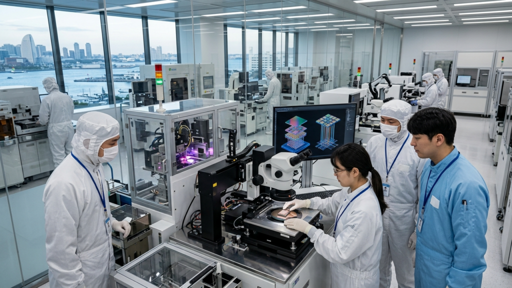
Samsung Electronics Establishes Advanced Packaging R&D Center in Yokohama to Deepen Collaboration with Japanese Suppliers for HBM Technologies
digitimes South Korea Overview Samsung Electronics has opened an advanced packaging research center in Yokohama, Japan, to strengthen development cooperation with Japanese suppliers of critical materials and equipment for HBM. This strat... -
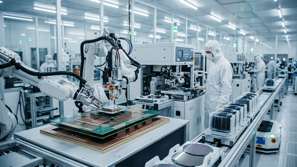
Scientech Sees 50% Surge in Advanced Packaging Equipment Shipments Driven by AI Demand; TSMC’s CoPoS Production Set for 2027 Launch
Taipei Times Taiwan Overview Scientech Corp, a supplier of advanced packaging equipment and reclaimed wafers, anticipates a 50% year-on-year increase in shipments for 2026, fueled by robust AI application demand and rapid technological s... -
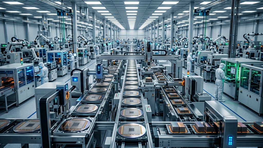
NVIDIA to Boost CoWoS Production Capacity by 3.5x to Over 120,000 Wafers/Month by End-2026, Securing HBM4 Supply
SemiconductorX USA Overview NVIDIA plans to scale its CoWoS (Chip-on-Wafer-on-Substrate) production capacity by 3.5x to 120,000–130,000 wafers per month by the end of 2026, up from 35,000, driven largely by its own demand. The company is... -
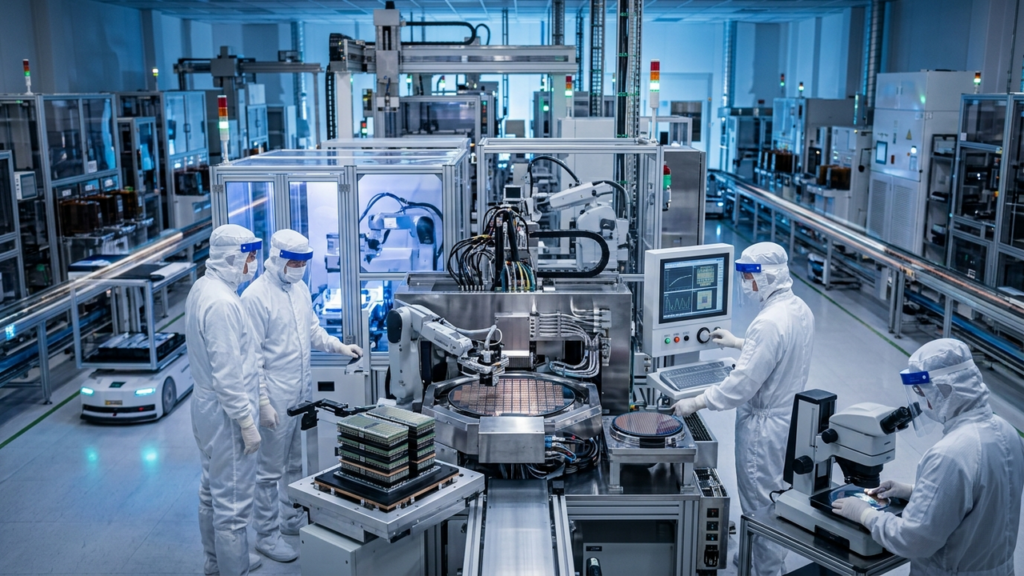
Samsung Foundry Unveils Next-Gen HBM Architecture Leveraging Advanced Packaging for AI/HPC Performance
Samsung Foundry South Korea Overview Samsung Foundry announced a new HBM architecture that combines advanced logic nodes with advanced packaging, promising significantly higher bandwidth and energy efficiency for AI and HPC systems. Its ... -
Semiconductor Back-End Weekly Report September 6, 2026
▼ ▼ ▼ If the infographic makes you want to read the full report, please click the download button below. ▼ ▼ ▼ 📄 Weekly Report September 06, 2026 (PDF) — Download Weekly Report September 06, 2026 (PDF) — DownloadDownload 🎙 Podcast Septe... -
Unimicron Reports 90% Surge in Equipment Demand from AI, Japanese SME Dependence on ABF Substrates Creates Bottleneck
BigGo Finance Taiwan Overview Unimicron Technology Chairman Chien Shan-Chieh stated that escalating AI demand has severely impacted the substrate sector, worsening supply-demand imbalance due to heavy reliance on small and medium-sized J... -
Amkor Technology and NVIDIA Announce $1.5 Billion Advanced Packaging Partnership to Accelerate AI Multi-Die Integration
IMAPS 3D InCites Content Platform USA Overview Amkor Technology and NVIDIA announced a multi-year partnership in July 2026, including a $1.5 billion advanced packaging and development agreement, to drive next-generation technology for AI... -
Dell Reports Record Q2 Revenue of $47 Billion with $95 Billion AI Server Backlog; Entire Supply Chain, Including DRAM, HBM, ABF Substrates, at ‘Redline’
KuCoin International Overview Dell reported record Q2 revenue of $47 billion and an impressive $95 billion backlog for AI servers. However, Dell executives stated that the entire supply chain, including DRAM, NAND, specific CPUs, mature ... -
TSMC SVP Reports 90% Surge in Equipment Orders in Six Months Driven by AI Demand: Equivalent to Building 20 Fabs Globally Simultaneously
TechSoda Taiwan Overview TSMC Senior VP Cliff Hou reported an astonishing 90% surge in equipment orders over six months, driven by AI demand far exceeding forecasts, equivalent to constructing nearly 20 fabs worldwide simultaneously. Uni... -
Simmtech to Invest 400 Billion Won in Next-Gen AI Server Substrate Production: Capacity Expansion Starts 2028
The Elec Inc. South Korea Overview Simmtech announced a phased 400 billion won (approx. $300 million) investment to expand production capacity for next-generation substrates used in AI servers. New facilities in Cheongju will boost outpu...