Semiconductor Back-End– category –
-

TSMC’s COUPE Platform for Co-Packaged Optics Targets 2026 Mass Production, Integrating Micro LEDs for AI Cluster Performance Boost
The Storm Media Taiwan Overview TSMC has announced the 2026 mass production launch of "COUPE" (Compact Universal Photonic Engine), an innovative platform for co-packaged optics (CPO) interconnects. Utilizing SoIC bonding to stack photoni... -
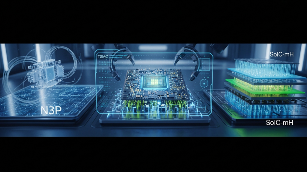
Apple’s M5 Ultra Pioneers Integration with TSMC’s N3P Process and SoIC-mH Packaging
TrendForce Taiwan Overview Reports indicate Apple's upcoming M5 Ultra chip, expected at WWDC, will likely leverage TSMC's N3P process node and its advanced SoIC-mH (System-on-Integrated-Chips – molded horizontal packaging) technology. So... -
Intel and Tesla Partner on AI6 Data Centers, Tapping Advanced Packaging for Production at Austin’s ‘Terafab’
Jamie's Substack USA Overview Tesla has announced a strategic partnership with Intel Foundry Services to scale its AI6 chip-powered data center clusters, extensively utilizing Intel's advanced packaging technologies. The collaboration wi... -
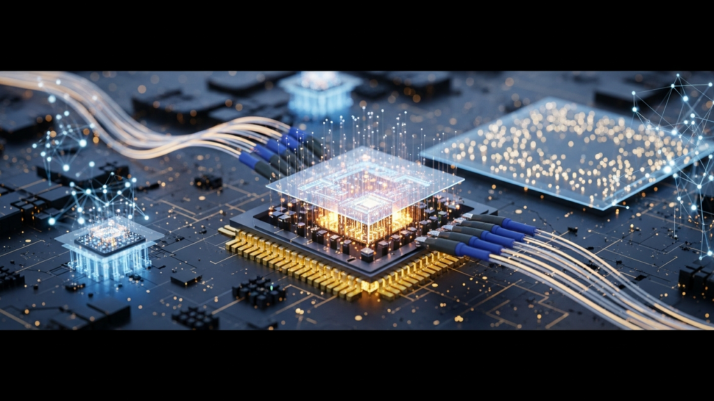
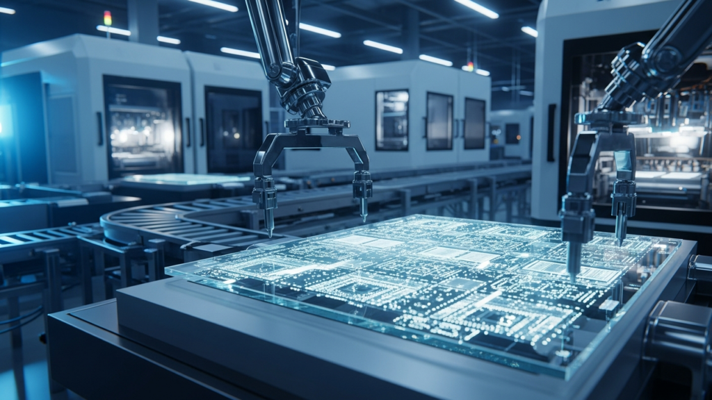
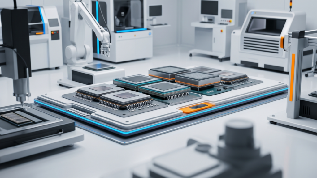
Advanced Packaging’s Evolution: 2.5D/3D Integration, Chiplets, and Hybrid Bonding Propel AI and HPC
Springer Professional Germany Overview Semiconductor packaging technology has dramatically evolved from 2D to 2.5D and 3D IC integration, a transformation accelerated by the explosive demand from AI and High-Performance Computing (HPC). ... -
Sub-10nm Residual Distortion Achieved in Low-Distortion Fusion Bonding with Pneumatically Curved Wafers for Advanced Semiconductors
arXiv USA Overview A recent arXiv publication reports the development of a novel low-distortion fusion bonding technique that employs pneumatically curved wafers to achieve an exceptionally low residual grid distortion of less than 10 na... -
Glass Substrates: The Next Frontier in AI Packaging and the Race to Mass Production
The Economy South Korea Overview Glass substrates are rapidly emerging as a transformative technology in advanced AI chip packaging, poised to replace conventional organic substrates and silicon interposers by offering superior dimension... -
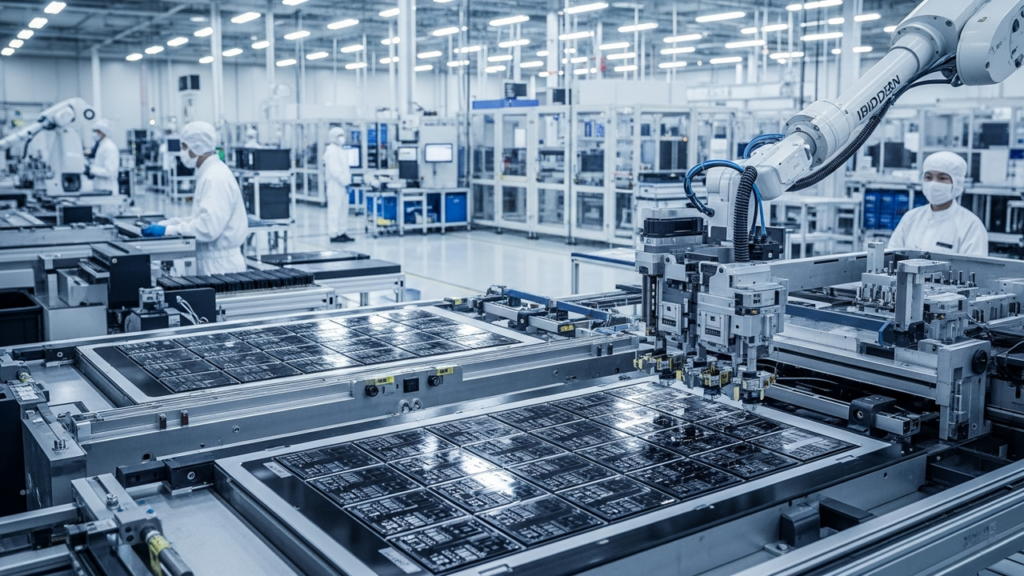
Ibiden and Unimicron Unveil Over $5 Billion Investment to Dramatically Expand AI Server ABF Substrate Production
Next Financial Japan Overview Japanese Ibiden and Taiwanese Unimicron are jointly investing over ¥800 billion (approximately $5 billion USD) to significantly increase production capacity for high-performance ABF (Ajinomoto Build-up Film)... -
Europe Boosts Investment in Advanced Packaging and Chiplet Integration; imec’s FAMES Pilot Line Aims to Mitigate Regional Supply Chain Risks
Astute Group UK Overview Europe is significantly increasing investment in advanced packaging and chiplet integration technologies to diversify its semiconductor supply chain and reduce regional procurement risks, shifting focus from pure... -
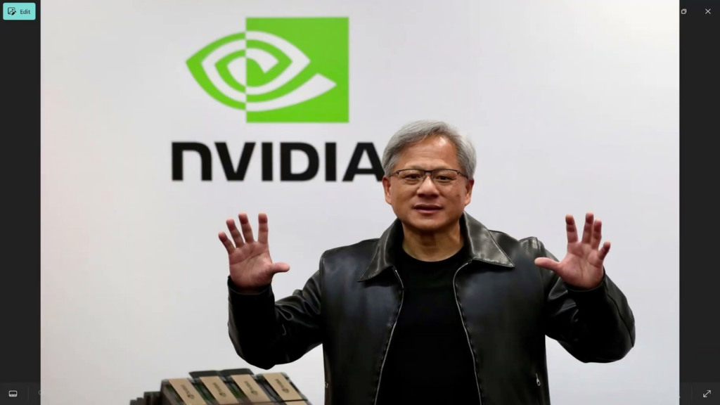
NVIDIA Locks Down Multi-Year HBM Supply Deals, Anticipating Persistent Shortages Beyond 2028
gagadget.com USA Overview NVIDIA CEO Jensen Huang recently visited South Korea, securing multi-year agreements with key partners including SK Hynix, SK Telecom, Naver, and Doosan Group for High Bandwidth Memory (HBM) supply, AI cloud inf... -
Amkor Bolsters U.S. Semiconductor Ecosystem with Over $7 Billion Investment in Arizona Advanced Packaging Facility
Amkor USA Overview Amkor Technology is dramatically escalating its commitment to a new advanced packaging and test facility in Peoria, Arizona, increasing its investment from an initial $2 billion to over $7 billion. This strategic expan...