Semiconductor Back-End– category –
-

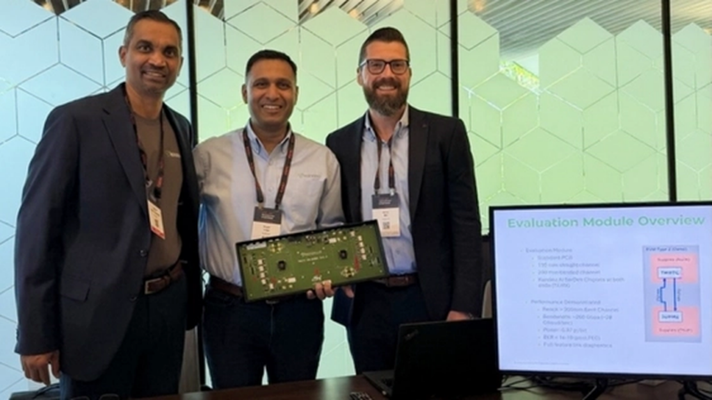
Cadence and Samsung Foundry Deepen 2nm and 3D-IC Collaboration to Meet Surging AI Infrastructure Demand
Chiplet News USA Overview Cadence and Samsung Foundry are deepening their collaboration in 2nm process technology and 3D-IC (3D Stacked Integrated Circuit) technology to address the surging demand for AI infrastructure and physical AI. T... -
Synopsys Enhances Power and Performance for AI and Multi-Die Designs on Latest Samsung Foundry Processes
Chiplet News USA Overview Synopsys announced solutions at SAFE Forum 2026 to enhance power efficiency and performance for AI and multi-die designs, leveraging Samsung Foundry’s latest process technologies. This initiative directly addres... -
Samsung Reportedly to Launch Physical AI Chiplet Platform Next Year, Accelerating AI Inference and Infrastructure
Design And Reuse South Korea Overview Samsung is reportedly planning to launch a physical AI chiplet platform as early as next year, aiming to accelerate next-generation chip development for AI inference and infrastructure. This platform... -
Fraunhofer IPMS Develops High-Density Chiplet Systems at Wafer Level, Advancing Integration for AI and HPC
Design And Reuse Germany Overview Fraunhofer IPMS has developed high-density chiplet systems at the wafer level, aiming to enhance integration for AI and high-performance computing (HPC) applications. This research contributes to the min... -
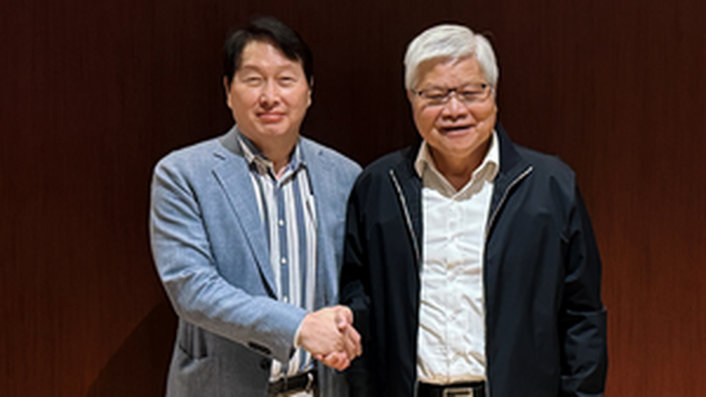
SK Group Chairman Deepens AI Alliances with Nvidia and TSMC, Expanding Next-Gen HBM and Advanced Packaging Collaboration
The Korea Herald South Korea Overview SK Group Chairman Chey Tae-won has strengthened alliances with leading AI chipmakers, meeting with Nvidia CEO Jensen Huang and later with TSMC Chairman C.C. Wei in Taiwan. Discussions focused on expa... -
Credo Completes DustPhotonics Acquisition, Bolstering Co-Packaged Optics (CPO) Solutions to Accelerate AI Data Centers
Advanced Packaging News USA Overview Credo has completed its acquisition of DustPhotonics, significantly strengthening its Co-Packaged Optics (CPO) solutions. This acquisition is poised to advance high-bandwidth, low-power interconnect t... -
Marvell Unveils Industry’s First 102.4 Tbps AI Switch, Doubling Bandwidth for AI Data Center Networks
Advanced Packaging News USA Overview Marvell announced the industry's first 102.4 Tbps AI switch, setting a new benchmark for network bandwidth in AI data centers. This innovative switch doubles bandwidth compared to current top-performi... -
Samsung Electronics to Invest $1.5 Billion in Vietnam Semiconductor Test Facility Amid Surging AI Chip Demand
Quintile Reports South Korea Overview Samsung Electronics announced plans to invest approximately $1.5 billion in a semiconductor testing facility in Vietnam to address the memory chip shortage caused by surging AI chip demand. This stra... -
Hybrid Bonding Unlocks New Frontiers in 3D Integration, Driving AI Accelerators and Chiplet Designs
PatSnap UK Overview Hybrid bonding, an innovative 3D integration technology, enables both electrical continuity and mechanical integrity without solder or microbumps by combining metal-to-metal (primarily Cu-Cu) and dielectric-to-dielect... -
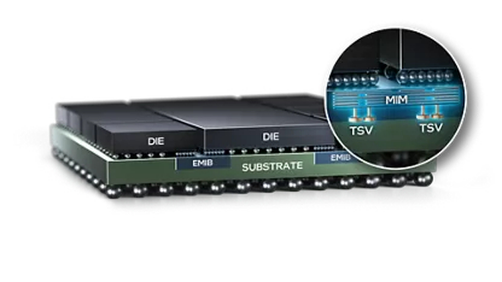
Intel Commits to Massive Advanced Packaging Push for Foundry Revival, EMIB Capacity Expansion Key
BusinessKorea USA Overview Intel is committing to a massive expansion of its advanced semiconductor packaging capabilities to accelerate its foundry business revival, with a core focus on expanding its proprietary EMIB (Embedded Multi-di...