COMPANY PROFILE / FUNCTIONAL MATERIALS
Metalenz
A privately held optics design company in Boston that makes flat “metalenses” in semiconductor fabs; its volume today rides on ST’s distance sensors, and its next test is the face-authentication product Polar ID
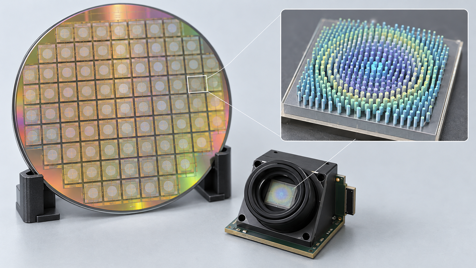
Metalenz designs metasurface optics (metalenses), a business built on work from Federico Capasso’s lab at Harvard University. Instead of grinding glass or molding plastic, it bends light with fine nanostructures patterned in a thin semiconductor layer. It is headquartered in Boston, Massachusetts, and is privately held. Its sales and profit could not be confirmed from official materials.
The company describes itself as a “fabless semiconductor optics company”. Its optical parts are made in the semiconductor fabs of STMicroelectronics (since 2022) and UMC (since 2023). In July 2025 ST said it had shipped well over 140 million metasurface optics and FlightSense modules using Metalenz IP since 2022. Polar ID, its polarization-based face authentication for smartphones, was announced in November 2025 as ready for volume production, but no phone model or customer using it could be confirmed from official materials.
This article draws on the company’s website and press releases (including joint announcements with STMicroelectronics and UMC), U.S. Securities and Exchange Commission (SEC) Form D filings, and a peer-reviewed paper, and sets out what could be confirmed and what could not. All performance figures are manufacturer’s stated values, and the test conditions are not published.
- At a glance: Metalenz and its place in functional materials
- Logo and naming
- Where the company sits in functional materials
- Company scale
- Resources committed to functional materials
- Track record
- Plans
- What the company is aiming for in functional materials
- Partnership map for functional materials
- Technologies, products and services
- Risks
- Glossary
- References
- Claim-to-source audit
1. At a glance: Metalenz and its place in functional materials
Massachusetts, U.S.205 Portland Street, Suite 600 (website). In March 2023 it announced a move that more than doubled its floor space
Components & devices (secondary)An optics design company; manufacturing is done by outside semiconductor fabs. It supplies elements and modules, and a full face-authentication system
(metalenses)Nanostructures in a single semiconductor layer control light. The company says it focuses on 940 nm (near-infrared). The material of the nanostructures could not be confirmed
UMC (from 2023)ST said “well over 140 million” shipped (July 2025). Metalenz’s own 2026 timeline says first-generation metasurfaces in the market “top 300 million”
Metalenz is one of the few cases where metasurface optics has actually gone into a product. In 2022 its optics were adopted in the lens section of ST’s FlightSense distance sensors, and in July 2025 ST said shipments of optics and modules using Metalenz IP had passed 140 million Sourced. Manufacturing is done in outside semiconductor fabs; ST makes them on 300 mm wafers.
However, no phone model carrying the face-authentication product Polar ID, no customer name, no shipment volume and no sales figure could be confirmed. “Ready for volume production” (November 2025) is an announcement of readiness, not of shipments. The performance figures (4x signal-to-noise ratio, 0% spoof acceptance and so on) are manufacturer’s stated values with no published baseline or conditions Not yet confirmed.
2. Logo and naming

The logo is the one shown at the top of the company’s official website (metalenz.com): a grid of dots shading from purple to pink, and the word “metalenz”. It is taken from the site as the original SVG image; it has not been recreated with generated images.
Naming: the company is Metalenz, and the legal entity is Metalenz, Inc. SEC Form D filings show “MetaLenz, Inc.” (capital L) in 2020 and “Metalenz, Inc.” in 2022. Polar ID, Polar 3D, PolarEyes, Orion and Gemini are the company’s product and brand names.
Official site: https://metalenz.com/3. Where the company sits in functional materials
Metalenz’s main type is startups & new approaches (commercializing a new principle, the metasurface), and its secondary type is components & devices (supplying optical elements and modules). It does not make the material or the element itself; it holds the design and the IP and leaves manufacturing to semiconductor fabs. It is the business form of the principles covered in our explainers on metalenses and flat optics and on metamaterials and metasurfaces. What the official materials confirm about its businesses is below.
| Business / product | Role at Metalenz | Primary information found | Status |
|---|---|---|---|
| Meta-optic elements for distance sensors | First volume product. Adopted in the lens section of ST’s direct time-of-flight (dToF) sensor VL53L8 (June 2022), and since then across ST’s FlightSense line | Joint ST-Metalenz announcements (June 2022, July 2025) | Sourced (joint announcement) |
| Structured-light projector elements (Orion) | Meta-optic elements that make a dot pattern. Used by Dilusense (smart locks, payment kiosks; July 2023); the Starlight projector with Vertilite (about 18,000 dots; September 2023) | Three company press releases | Sourced (company statement) |
| Polarization face authentication, Polar ID | A polarization-sensitive meta-optic built directly onto the image sensor judges, from one image, a face and whether it is a live person. UMC “ready for volume production” announced in November 2025; an under-display version in May 2026 | Company press releases; joint announcement with UMC | Sourced (company statement) / the phones using it could not be confirmed |
| Polar 3D | An application of the same element: shape and reflection from one image, for relightable selfies and 3D data for avatars (February 2026) | Company press release (February 2026) | Not yet confirmed (no customer named) |
| Automotive, robotics and others | The website lists uses (driver assistance, driver monitoring, material identification, bin picking). No customers or adoptions could be found | Use pages on the website | Sourced (list of uses) / adoption not confirmed |
4. Company scale
Metalenz is privately held and publishes no financial statements. The scale that company materials and SEC Form D filings allow us to confirm is shown below Sourced.
| Item | What was confirmed |
|---|---|
| Sales, profit, debt | Not disclosed. Not stated on the website, in press releases or in Form D filings |
| Employees | In March 2023 the company said it had more than 40 full-time staff, over half in design and engineering. The current figure could not be confirmed |
| Founding / headquarters | Founded in 2016 by Rob Devlin and Federico Capasso (company timeline). It came out of stealth in February 2021. It moved its headquarters to downtown Boston in 2020 and announced a move to a space more than twice as large in March 2023 |
| Leadership | Co-founder and CEO: Rob Devlin (Ph.D. in applied physics in Capasso’s lab at Harvard). CTO: Pawel Latawiec. VP Operations: Mari-Anne Gagliardi. VP Module Technology: Hao Zhou. VP Software and Systems Engineering: Julian Gorfajn. CFO: Brad MacMullin. A General Counsel is also listed. A June 2024 release named Gaurav Aggarwal as VP of software and systems; the leadership page checked in October 2026 lists Julian Gorfajn in that role |
| Intellectual property | The company says it holds an exclusive worldwide license to the foundational metasurface patent portfolio from Harvard University. Patent counts are described as growing over time: 15 issued patents in 2021, “20+” in 2022, and “more than 150 patent applications and issued patents” in August 2025 |
| Funding (announced amounts) | US$10 million in February 2021; US$30 million (Series B) in October 2022. The US$40 million total is our calculation; later funding could not be confirmed from official materials Our calculation |
| Shipments (company and ST) | ST: “well over 140 million” since 2022 (July 2025). Metalenz: “more than 140 million” (November 2025); its 2026 timeline says first-generation metasurfaces in the market “top 300 million”. The scope of the count and the as-of dates are not given |
The company’s and ST’s releases cite a forecast that the metasurface optics market will “reach US$2 billion by 2029” from a 2024 report by the research firm Yole Group. This article does not use market-research estimates. Expressions such as “world’s first” and “first to commercialize” are the company’s own, and independent verification was not checked here. We make no judgment on rankings or superiority relative to other companies.
5. Resources committed to functional materials
Because the company is privately held, disclosure of amounts is limited. The four points of people, money, external moves, and universities and public funding are set out below, showing what could and could not be confirmed.
| Item | What was confirmed | Status |
|---|---|---|
| People (R&D base and staff) | Design and engineering are based at the Boston headquarters. In March 2023: more than 40 full-time staff, over half in design and engineering. The research origin is Capasso’s lab at Harvard. Current R&D headcount is not disclosed | Sourced / current headcount not confirmed |
| Money (R&D spend, capital spending, funding) | Actual R&D spend and capital spending are not disclosed. The company owns no fab and uses outside semiconductor fabs. Funding: US$10 million in February 2021 (3M Ventures, Applied Ventures, Intel Capital, M Ventures, TDK Ventures, Tsingyuan Ventures, Braemar Energy Ventures); US$30 million in October 2022 (led by Neotribe Ventures, with Foothill Ventures, M Ventures, Intel Capital, Osage University Partners, TDK Ventures, 3M Ventures, Global Brain, SG Innovate, Hegemon Capital and Braemar Energy Ventures). Form D filings report about US$7.36 million in 2020 (19 investors) and about US$29.0 million in 2022 (16 investors) | Sourced / actual spend not disclosed |
| External investments, acquisitions, joint ventures, divestments | No investment, acquisition, joint venture or divestment by Metalenz in another company could be confirmed. Its investors are listed above; investors such as TDK, 3M and Intel appear as investors, but no business partnership with them could be found. Samsung is a sensor supplier for Polar ID; it is not listed as an investor | Not confirmed (its own investments) |
| Universities, research institutes, public funding | University: Harvard University (exclusive license to the foundational patents from Capasso’s lab; Capasso is a co-founder). Public funding: no government grant or subsidy could be confirmed from official materials. Osage University Partners (a fund that invests in university-origin technology) is a private investor | University: Sourced / public funding not confirmed |
Status of main products and facilities
The table below covers what could be confirmed from announcements by the company, ST and UMC. Production capacity (wafers, units) is not disclosed in any case, so no figures are compared.
| Product / facility | Where and how it is made | Scale (stated) | Stage | Date and source |
|---|---|---|---|---|
| Meta-optic elements for FlightSense | On silicon wafers in ST’s front-end semiconductor fabs (2022); the July 2025 announcement describes ST’s 300 mm wafer lines | “Well over 140 million” (ST, July 2025). Metalenz: “top 300 million” (2026) | Operating (shipping) | ST-Metalenz announcements (June 2022, July 2025) |
| Direct supply via UMC (Orion and others) | Moved to volume production at UMC’s 12-inch (300 mm) fab in Singapore (June 2023) | Not disclosed | Moved to volume production (announced June 2023; first customer Dilusense) | Announcements of June and July 2023 |
| Polar ID (element integrated with the sensor) | UMC makes the meta-optic layer on a 40 nm process and bonds it to the sensor wafer-on-wafer; 300 mm wafers | Not disclosed | Ready for volume production (November 2025). Not yet confirmed (shipments not confirmed) | Joint UMC-Metalenz announcement (November 2025) |
| Under-display Polar ID | No manufacturing detail given | Not disclosed | Demonstrated (May 2026, Display Week) | Metalenz announcement (May 2026) |
6. Track record
| When | What happened | Meaning |
|---|---|---|
| 2016 | Founded by Rob Devlin and Federico Capasso. Exclusive license to Harvard IP obtained. First high-quality images captured with metasurfaces (company timeline). The same year Devlin and colleagues in Capasso’s lab reported visible-light metalenses in Science (Khorasaninejad et al.) | Starting point from research to business |
| 2018 and 2020 | First high-volume manufacturing demonstration wafers (2018). “Single metasurface imaging” invented, and a headquarters move (2020; company statements). A Form D for about US$7.36 million (May 2020) | Checking a volume process |
| 2021 | 4 February: out of stealth, US$10 million raised. May: Orion dot projector. 2 June: co-development and license agreement with ST covering manufacturing process development, industrialization and licensing; ready for mass production “by the end of this year” | Securing a manufacturing partner |
| 2022 | January: PolarEyes and Gemini announced. 9 June: adopted in ST’s VL53L8 and brought to market (the company says this was the first time metasurface technology became commercially available). October: Series B (US$30 million) | First volume adoption (about half a year after the “end of 2021” expectation) |
| 2023 | March: headquarters move, more than 40 full-time staff. June: supply chain for the “open market” with UMC (first customer Dilusense). July: Dilusense; September: Vertilite. 26 October: Polar ID announced (demonstrated on a Qualcomm reference phone) | From ST-routed supply to direct supply to customers |
| 2024 | February: Samsung’s ISOCELL Vizion 931 image sensor chosen for Polar ID (MWC); “under early evaluation with several leading smartphone makers”. June: leadership hires ahead of volume production | Polar ID’s part list settles |
| 2025 | 10 July: new license agreement with ST. August: patent portfolio expanded (over 150). 12 November: Polar ID ready for volume production at UMC | Manufacturing widened |
| 2026 | February: Polar 3D. 4 May: under-display Polar ID announced (demonstrated at Display Week). Timeline: “first generation top 300 million” | Applications widened |
7. Plans
(no shipment date given)November 2025 announcement. Which phone makers will adopt it, and when, is not stated
The website lists uses in automotive (driver assistance, driver monitoring), smart home and industrial robotics (material identification, transparent-object detection, bin picking) and remote diagnostics (polarization imaging on a smartphone). These are lists of uses, not confirmed adoptions or plans Not yet confirmed.
None of the following is stated in primary sources Not yet confirmed.
Sales, profit, headcount, R&D spend; the phone models, customers and timing for Polar ID; Polar ID shipment volume, yield and cost; UMC’s capacity; the material and thickness of the metasurface nanostructures; the test conditions for each stated figure (4x signal-to-noise, 0% spoof acceptance, 50% size and cost reduction); whether any funding followed October 2022; the amount, term and exclusivity of the ST agreements; adoption in automotive or robotics.
8. What the company is aiming for in functional materials
This section includes points the company does not state directly. They are set out as inferences, within what the primary information allows, with their grounds.
| What can be read | Primary information behind it | Status |
|---|---|---|
| Its core is moving optics production onto semiconductor lines (“printing lenses like computer chips”) | Phrases repeated on the website and in releases (“shifting optics production into the semiconductor foundry”); ST’s 300 mm lines; volume production at UMC’s 12-inch fab; the design that builds the Polar ID element directly on the image sensor | Sourced (company statement) / the positioning is an Inference |
| It is shifting weight from parts that replace components via ST to its own full system (Polar ID) | 2022 centered on an element inside a distance sensor; from 2023 Polar ID is front and center, described as “full-stack” including algorithms (August 2025). The June 2024 hires strengthen software and operations | Inference |
| It treats polarization as the axis that differentiates metasurfaces | PolarEyes (2022), Polar ID (2023) and Polar 3D (2026) are applications of the same polarization-sensing element. The company says conventional optics cannot capture polarization information | Sourced (company statement) / the intent is an Inference |
| It is widening the ST agreement and adding manufacturing partners to secure supply and give customers choices | ST in 2021, UMC in 2023, the new ST license in July 2025, Polar ID at UMC in November 2025 | Inference |
The reading that the company is “moving weight from ST-routed parts to its own system” rests on how the subject of its announcements has changed. The June 2022 joint announcement was about replacing a lens section inside ST’s distance sensors. From June 2023 a “open-market” supply chain with UMC and direct supply to customers such as Dilusense were added, and from October 2023 Polar ID (the polarization element, the sensor and the algorithms together) came to the fore. The August 2025 announcement says its patents span “the design and manufacture of metasurfaces, as well as chips, modules, products, and image processing”.
That said, official materials do not allow us to say the relationship with ST has shrunk, because a new license agreement was signed in July 2025. This is our reading of what the announcements say Not yet confirmed.
9. Partnership map for functional materials
The company’s relationships are characterized by relying on two semiconductor fabs, ST and UMC, for manufacturing, and creating value through design and IP. No joint venture or acquisition with an operating company could be confirmed. No customer naming Polar ID could be confirmed; the only statement is that several leading OEMs are evaluating it Not yet confirmed.
10. Technologies, products and services
What follows is what the company’s official materials state. All figures are manufacturer’s stated values; where the materials give no baseline or conditions, that is noted. They do not rank any product against others, and values under different conditions cannot be compared. For the principles, see our explainers on metalenses and flat optics and on metamaterials and metasurfaces Sourced.
| Item | Manufacturer’s stated value or description | Basis and conditions (as given in the materials) |
|---|---|---|
| Combining optical functions | Up to five optical functions combined in one meta-optic (technology page). The functions of three or four lenses and components in one flat element (company description) | Which application, which wavelength: not stated |
| Signal-to-noise in 3D imaging | “4x improvement in signal to noise in 3D imaging systems” (technology page) | The comparison baseline (which conventional approach) and conditions are not stated |
| Stray light, low f-number, temperature | Substantially less stray light than conventional diffractive optical elements (DOEs), and higher imaging performance at low f-number and across temperature (company statement) | No figures given |
| Wavelength | Production currently focused on 940 nm applications. An anti-reflection (AR) coating is applied to maximize transmission | FAQ statement |
| Operating temperature | “Exceptionally large, including automotive ranges (e.g. -40 C to 110 C)”. Inorganic materials with very low thermal expansion; layered deposition means no delamination (FAQ) | No test standard or duration given. “e.g.” means this is not a guaranteed value |
| Solder reflow | “Reflow compatible, extreme temperature stability” (technology page) | Reflow temperature and number of passes not given |
| Manufacturing | A single mask layer on existing semiconductor equipment (technology page). UMC makes the element layer on a 40 nm process and bonds it to the sensor wafer-on-wafer (November 2025) | Yield and mask detail not given |
| Polar ID security and size | One polarization sensor and one 940 nm illuminator. “0% spoof acceptance rate” (May 2026). A 50% size and cost reduction compared with traditional face unlock (February 2024) | The attack methods and test are not stated. The 50% baseline is described as traditional structured-light approaches, with no model or conditions given |
| Projector (Orion 18K) | About 18,000 pseudorandom dots, combined with 391 Vertilite VCSEL emitters at 940 nm | September 2023 announcement |
(1) What it is made of: the official materials do not name the material. The company says “a single semiconductor layer”, “inorganic materials” and “nanopillars”, but gives no material (for example silicon-based or a metal oxide), no film thickness and no pillar dimensions. A 2016 paper in Science (Khorasaninejad et al.) reported visible-light metalenses made of titanium dioxide (TiO2) nanostructures, as that journal’s commentary describes in its Crossref record. Whether today’s products use the same material cannot be confirmed from official materials.
(2) The key to manufacturing is that semiconductor processes can make the optic. UMC says the element layer is made on a 40 nm process, and ST says it uses 300 mm wafers. One reading is that 40 nm is a generation fine enough for features suited to 940 nm light. That is commentary; the actual pillar dimensions are not published. The fundamental difference from glass or plastic lenses is that the element is made with semiconductor-grade alignment precision.
(3) Design constraints tie to wavelength and polarization. The company’s focus on 940 nm is consistent with the nanostructure dimensions being set for the wavelength in use. Using the same element for full-color imaging across the visible band runs into chromatic dispersion, covered in our explainer on metalenses and flat optics; the company’s materials do not center on color imaging. An element that measures polarization is described as sorting light by polarization through anisotropic nanostructure shapes, which adds design freedom and also sensitivity to manufacturing variation (commentary; tolerances are not published).
(4) Reading the numbers. “4x signal-to-noise”, “50% reduction” and “0% spoof acceptance” are given without baselines or conditions, so they are not on the same conditions as each other or as other companies’ values. This article does not judge superiority over other approaches.
11. Risks
| Risk | Detail | Status |
|---|---|---|
| Opaque finances | Sales, profit, debt and cash are not in official materials. The last announced funding was in October 2022, and later funding plans cannot be confirmed. This article cannot assess financial health | Not confirmed |
| Dependence on manufacturing partners | Manufacturing depends on ST and UMC; the company has no fab of its own. The new ST license (July 2025) lets ST use the company’s IP more widely; the revenue split and exclusivity are not disclosed | Sourced (company statement) / contract terms not confirmed |
| Opaque main customers | Most shipments are probably ST-routed distance sensors, but the share is not disclosed. No phone model using Polar ID is in official materials. When “evaluating” will become “adopted” cannot be confirmed | Not confirmed / Inference |
| Gap between plan and result | The June 2021 joint announcement said mass-production readiness by the end of 2021, and the market launch was announced in June 2022. For Polar ID, the October 2023 and February 2024 announcements said “under early evaluation with several OEMs”, and the “ready for volume production” announcement came in November 2025. No phone carrying it can be confirmed | Sourced (dates) / assessment Not yet confirmed |
| Competing technologies and alternatives | Face authentication coexists with structured light, 2D face recognition and other approaches. The advantage of meta-optics is the company’s claim and this article does not compare. Other companies’ developments were not checked here | Not confirmed |
| Unverified claims | “World’s first”, “first to commercialize”, “0% spoof acceptance”, “4x signal-to-noise” and “over 300 million shipped” are the company’s claims, with no independent verification, baseline or counting scope in the materials. ST’s “well over 140 million” and the company’s “top 300 million” appear to have different as-of dates, which are not stated | Sourced (company statement) / verification not confirmed |
| IP dependence | The foundational patents rest on an exclusive license from Harvard University. The terms and duration are not disclosed. Patent counts are described as growing, but validity and any disputes were not checked here | Sourced (company statement) / not confirmed |
12. Glossary
- Metasurface (meta-optics)
- A thin surface patterned with structures smaller than the wavelength of light, controlling the phase, intensity and polarization of light. A metalens is one kind.
- Nanopillar
- A nanometer-scale pillar. The width, shape and height of the pillar change the phase of light passing through.
- dToF (direct time of flight)
- A method that measures distance by directly timing the round trip of emitted light. FlightSense is ST’s product line name.
- Structured light
- A 3D measurement method that projects a pattern such as dots and reads shape from the distortion of the pattern. It needs a projector (the part that makes the dots).
- Polarization
- The direction in which light oscillates. It changes with surface and material, and the company says it can help tell a real face from a mask.
- Fabless
- A business model with no manufacturing plant of its own, focusing on design and contracting manufacturing to outside semiconductor fabs.
- Reflow
- The step in which a whole board is passed through a hot oven to solder components. Parts must withstand that heat.
- SEC Form D
- A notice filed with the SEC in the United States when a private (non-public) funding round is made. It shows the amount and number of investors, not sales.
- Manufacturer’s stated value
- A description or performance figure given by the manufacturer itself. It cannot be compared with other products unless the test conditions and version are the same.
13. References
- Metalenz Official website (home page; address, patent count, latest news; source of the logo image). https://metalenz.com/
- Metalenz Official website, “About Us”. Timeline (2016 to 2026) and company description. https://metalenz.com/about-us/
- Metalenz Official website, “Leadership”. https://metalenz.com/leadership/
- Metalenz Official website, “Foundational Technology”. Technology, relationship with ST, manufacturing. https://metalenz.com/our-technology/
- Metalenz Official website, “What are Meta-Optics”. Features and FAQ (wavelength, anti-reflection coating, operating temperature). https://metalenz.com/what-are-meta-optics/
- Metalenz Official website, “PolarEyes”. Polarization imaging. https://metalenz.com/polareyes-polarization-imaging-system/
- Metalenz Official website, “Polar ID”. Configuration and features (manufacturer’s stated values). https://metalenz.com/polareyes-polarization-imaging-system/polar-id/
- Metalenz Official website, “Automotive”, “Consumer Electronics” and “Smart Home and Industrial Robotics”. Lists of uses. https://metalenz.com/automotive/
- Metalenz Metalenz Launches with $10M from 3M, Applied Ventures, Intel Capital, M Ventures, and TDK to Power the Next Generation of Smartphone Sensors (press release, 4 February 2021). https://metalenz.com/metalenz-launches-with-10m-from-3m-applied-ventures-intel-capital-m-ventures-and-tdk-to-power-the-next-generation-of-smartphone-sensors/
- STMicroelectronics and Metalenz STMicroelectronics and Metalenz Partner to Transform Optical Sensing for Consumer, Automotive, and Industrial Applications (joint announcement, 2 June 2021; posted on Metalenz’s website). https://metalenz.com/metalenz-partners-with-stmicroelectronics-to-develop-manufacturing-processes/
- STMicroelectronics and Metalenz Metalenz and STMicroelectronics Deliver World’s First Optical Metasurface Technology for Consumer Electronics Devices (joint announcement, 9 June 2022). https://metalenz.com/metalenz-and-stmicroelectronics-deliver-worlds-first-optical-metasurface-technology-for-consumer-electronics-devices/
- Metalenz Metalenz Raises $30 Million Series B Led by Neotribe Ventures (press release, 12 October 2022). https://metalenz.com/metalenz-raises-30-million-series-b-led-by-neotribe-ventures/
- Metalenz Metalenz Relocates Headquarters, Doubles Footprint, and Grows Team to Meet Increasing Demand for its Metasurface Optics (press release, 13 March 2023). https://metalenz.com/metalenz-relocates-headquarters-doubles-footprint-and-grows-team-to-meet-increasing-demand-for-its-metasurface-optics/
- Metalenz Metalenz Launches its Metasurface Optics on the Open Market in Partnership with UMC (press release, 26 June 2023). https://metalenz.com/metalenz-launches-its-metasurface-optics-on-the-open-market-in-partnership-with-umc/
- Metalenz and Dilusense Metalenz and Dilusense Partner to Revolutionize the Optics and Performance of Structured Light Sensing Systems (10 July 2023). https://metalenz.com/metalenz-and-dilusense-partner-to-revolutionize-the-optics-and-performance-of-structured-light-sensing-systems/
- Metalenz and Vertilite Metalenz and Vertilite Unveil “Starlight” Projector for Structured Light Applications using a New Meta-Optic (5 September 2023). https://metalenz.com/metalenz-and-vertilite-unveil-starlight-projector-for-structured-light-applications-using-a-new-meta-optic/
- Metalenz Metalenz Launches Polar ID, Enabling Simple, Secure Face Unlock for Smartphones (press release, 26 October 2023). https://metalenz.com/metalenz-launches-polar-id-enabling-simple-secure-face-unlock-for-smartphones/
- Metalenz Metalenz Confirms Samsung ISOCELL Vizion Image Sensor as Light-Engine for Polar ID (press release, 26 February 2024). https://metalenz.com/metalenz-confirms-samsung-isocell-vizion-image-sensor-as-light-engine-for-polar-id-the-worlds-smallest-most-affordable-and-secure-face-unlock-solution/
- Metalenz Metalenz Announces Key Leadership Appointments as Company Readies Polar ID for Mass Production (press release, 10 June 2024). https://metalenz.com/metalenz-announces-key-leadership-appointments-as-company-readies-polar-id-for-mass-production/
- STMicroelectronics and Metalenz STMicroelectronics and Metalenz Sign a New License Agreement to Accelerate Metasurface Optics Adoption (joint announcement, 10 July 2025). https://metalenz.com/stmicroelectronics-and-metalenz-sign-a-new-license-agreement-to-accelerate-metasurface-optics-adoption/
- Metalenz Metalenz Expands Its Technologies in the Metasurface Market to Include System Level Sensing Applications (press release, 18 August 2025). https://metalenz.com/metalenz-expands-its-technologies-in-the-metasurface-market-to-include-system-level-sensing-applications/
- Metalenz and UMC Metalenz and UMC Bring Breakthrough Face Authentication Solution Polar ID to Mass Production (joint announcement, 12 November 2025). https://metalenz.com/metalenz-and-umc-bring-breakthrough-face-authentication-solution-polar-id-to-mass-production/
- Metalenz Polar 3D from Metalenz delivers relightable selfies and realistic avatars on device from a single image (press release, 23 February 2026). https://metalenz.com/polar-3d-from-metalenz-delivers-relightable-selfies-and-realistic-avatars-on-device-from-a-single-image/
- Metalenz Polar ID kills the cutout – Metalenz launches simple, secure, face authentication working under the phone display (press release, 4 May 2026). https://metalenz.com/polar-id-kills-the-cutout-metalenz-launches-simple-secure-face-authentication-working-under-the-phone-display/
- U.S. Securities and Exchange Commission Metalenz, Inc. Form D (signed 2022; filed 5 October 2022; amount sold US$28,999,997, 16 investors). https://www.sec.gov/Archives/edgar/data/1813614/000156761922018246/primary_doc.xml
- U.S. Securities and Exchange Commission MetaLenz, Inc. Form D (signed 31 May 2020; amount sold US$7,360,746, 19 investors). https://www.sec.gov/Archives/edgar/data/1813614/000156761920011440/primary_doc.xml
- Khorasaninejad, M.; Chen, W. T.; Devlin, R. C.; Oh, J.; Zhu, A. Y.; Capasso, F. Metalenses at visible wavelengths: Diffraction-limited focusing and subwavelength resolution imaging. Science 352, 1190-1194 (June 2016). DOI checked in Crossref. https://doi.org/10.1126/science.aaf6644
14. Claim-to-source audit
| Claim in the text | Category | Source |
|---|---|---|
| Founding (2016, Devlin and Capasso), exclusive Harvard IP license, timeline (2018 demonstration wafers, 2020 single-metasurface imaging and move, milestones 2021 to 2026), “first generation top 300 million”, awards | Sourced (company statement) | Reference 2 https://metalenz.com/about-us/ |
| Headquarters address (205 Portland Street), more than 150 patents, latest news | Sourced (company statement) | Reference 1 https://metalenz.com/ |
| Leadership (CEO, CTO, VPs, CFO, General Counsel) | Sourced (company statement) | Reference 3 https://metalenz.com/leadership/ |
| Up to five optical functions combined, 4x signal-to-noise, replacement in ST’s FlightSense, single mask layer, “140 million” | Sourced (manufacturer’s stated value) | Reference 4 https://metalenz.com/our-technology/ |
| 940 nm wavelength, anti-reflection coating, operating temperature (-40 to 110 C as an example), difference from Fresnel lenses, reflow compatibility | Sourced (manufacturer’s stated value) | Reference 5 https://metalenz.com/what-are-meta-optics/ |
| PolarEyes functions (polarization, material discrimination, glare removal) | Sourced (manufacturer’s stated value) | Reference 6 https://metalenz.com/polareyes-polarization-imaging-system/ |
| Polar ID configuration (one polarization camera, one 940 nm illuminator) and its described features | Sourced (manufacturer’s stated value) | Reference 7 https://metalenz.com/polareyes-polarization-imaging-system/polar-id/ |
| Lists of uses such as automotive, robotics and remote diagnostics | Sourced (list of uses) | Reference 8 https://metalenz.com/automotive/ |
| US$10 million raised in February 2021 and its investors, 15 patents, exit from stealth | Sourced (company statement) | Reference 9 https://metalenz.com/metalenz-launches-with-10m-from-3m-applied-ventures-intel-capital-m-ventures-and-tdk-to-power-the-next-generation-of-smartphone-sensors/ |
| June 2021 co-development and license agreement with ST; mass-production readiness “by the end of this year” | Sourced (joint announcement) | Reference 10 https://metalenz.com/metalenz-partners-with-stmicroelectronics-to-develop-manufacturing-processes/ |
| Adoption in the VL53L8 (June 2022), manufacture in ST’s front-end fabs, ST’s FlightSense shipments of over 1.7 billion units | Sourced (joint announcement) | Reference 11 https://metalenz.com/metalenz-and-stmicroelectronics-deliver-worlds-first-optical-metasurface-technology-for-consumer-electronics-devices/ |
| Series B of October 2022 (US$30 million, led by Neotribe) and investors, more than 20 patents | Sourced (company statement) | Reference 12 https://metalenz.com/metalenz-raises-30-million-series-b-led-by-neotribe-ventures/ |
| March 2023 headquarters move, more than 40 full-time staff, over half in design and engineering | Sourced (company statement) | Reference 13 https://metalenz.com/metalenz-relocates-headquarters-doubles-footprint-and-grows-team-to-meet-increasing-demand-for-its-metasurface-optics/ |
| Move to volume production at UMC’s 12-inch fab in Singapore; first customer Dilusense | Sourced (company statement) | Reference 14 https://metalenz.com/metalenz-launches-its-metasurface-optics-on-the-open-market-in-partnership-with-umc/ |
| Adoption by Dilusense (Orion, more than 30,000 dots, smart locks and payment kiosks) | Sourced (joint announcement) | Reference 15 https://metalenz.com/metalenz-and-dilusense-partner-to-revolutionize-the-optics-and-performance-of-structured-light-sensing-systems/ |
| Starlight projector (about 18,000 dots, 391 VCSEL emitters, 940 nm) | Sourced (joint announcement) | Reference 16 https://metalenz.com/metalenz-and-vertilite-unveil-starlight-projector-for-structured-light-applications-using-a-new-meta-optic/ |
| Polar ID announcement (October 2023), demonstration on a Qualcomm Snapdragon 8 Gen 3 reference phone, several OEMs evaluating, evaluation kits in early 2024 | Sourced (company statement) | Reference 17 https://metalenz.com/metalenz-launches-polar-id-enabling-simple-secure-face-unlock-for-smartphones/ |
| Adoption of Samsung’s ISOCELL Vizion 931 (February 2024); the claimed 50% size and cost reduction | Sourced (manufacturer’s stated value) | Reference 18 https://metalenz.com/metalenz-confirms-samsung-isocell-vizion-image-sensor-as-light-engine-for-polar-id-the-worlds-smallest-most-affordable-and-secure-face-unlock-solution/ |
| June 2024 hires (VP software, VP operations) ahead of volume production | Sourced (company statement) | Reference 19 https://metalenz.com/metalenz-announces-key-leadership-appointments-as-company-readies-polar-id-for-mass-production/ |
| July 2025 new license with ST, ST’s 300 mm lines, ST’s “well over 140 million since 2022”, the Yole market forecast quoted (not used here) | Sourced (joint announcement) | Reference 20 https://metalenz.com/stmicroelectronics-and-metalenz-sign-a-new-license-agreement-to-accelerate-metasurface-optics-adoption/ |
| Expanded patent portfolio (over 150 applications and patents), the full-stack description (August 2025) | Sourced (company statement) | Reference 21 https://metalenz.com/metalenz-expands-its-technologies-in-the-metasurface-market-to-include-system-level-sensing-applications/ |
| Polar ID ready for volume production (UMC, 40 nm, wafer-on-wafer bonding, 300 mm), “more than 140 million” | Sourced (joint announcement) / volume production Not yet confirmed | Reference 22 https://metalenz.com/metalenz-and-umc-bring-breakthrough-face-authentication-solution-polar-id-to-mass-production/ |
| Polar 3D announcement (February 2026), planned demonstration at MWC | Sourced (company statement) / adoption Not yet confirmed | Reference 23 https://metalenz.com/polar-3d-from-metalenz-delivers-relightable-selfies-and-realistic-avatars-on-device-from-a-single-image/ |
| Under-display Polar ID (May 2026) and the claimed 0% spoof acceptance rate | Sourced (manufacturer’s stated value) | Reference 24 https://metalenz.com/polar-id-kills-the-cutout-metalenz-launches-simple-secure-face-authentication-working-under-the-phone-display/ |
| 2022 Form D (about US$29.0 million sold, 16 investors), Boston headquarters | Sourced | Reference 25 https://www.sec.gov/Archives/edgar/data/1813614/000156761922018246/primary_doc.xml |
| 2020 Form D (about US$7.36 million sold, 19 investors; the name written “MetaLenz, Inc.”) | Sourced | Reference 26 https://www.sec.gov/Archives/edgar/data/1813614/000156761920011440/primary_doc.xml |
| The 2016 Science paper (visible-light metalenses; the journal’s commentary describes titanium dioxide nanostructures): bibliographic details | Sourced (peer-reviewed paper) | Reference 27 https://doi.org/10.1126/science.aaf6644 |
| Cumulative funding of US$40 million (US$10 million plus US$30 million) | Our calculation | Our calculation (the sum of the announced amounts in References 9 and 12; later funding could not be confirmed) |
| Current sales, profit and headcount; Polar ID phone models, customers and shipment volume; element material and thickness; test conditions for each figure; funding after October 2022; ST contract amount and term; automotive and robotics adoption | Not yet confirmed | This article’s summary and outlook (items that could not be confirmed in primary sources; this article) |
| The readings that the core is moving optics production onto semiconductor lines, that weight is moving from ST-routed parts to a full system, that polarization is the differentiating axis, and that adding manufacturing partners secures supply | Inference | References 4, 11, 14, 20, 21, 22 https://metalenz.com/our-technology/ https://metalenz.com/metalenz-and-stmicroelectronics-deliver-worlds-first-optical-metasurface-technology-for-consumer-electronics-devices/ https://metalenz.com/metalenz-launches-its-metasurface-optics-on-the-open-market-in-partnership-with-umc/ https://metalenz.com/stmicroelectronics-and-metalenz-sign-a-new-license-agreement-to-accelerate-metasurface-optics-adoption/ https://metalenz.com/metalenz-expands-its-technologies-in-the-metasurface-market-to-include-system-level-sensing-applications/ https://metalenz.com/metalenz-and-umc-bring-breakthrough-face-authentication-solution-polar-id-to-mass-production/ |
| Classifying Metalenz as “Startups & new approaches (main), Components & devices (secondary)”, the four-type grouping, and the glossary | Our calculation | This article’s own grouping and outlook (this article) |
| A materials engineer’s view (the material not being named, the meaning of the semiconductor process, design constraints tied to wavelength and polarization, reading the numbers) | Commentary | Commentary by this article (company materials read from a materials viewpoint; this article) |
Last updated: 10 October 2026 / Troy Technical
This article is based on Metalenz’s website and press releases (including joint announcements with STMicroelectronics and UMC), SEC Form D filings and a paper in Science. It does not use market-research estimates or press-report figures. Passages marked “Inference” are our own readings of primary information, not company statements. Product performance figures are the company’s stated values and cannot be compared with values measured under other conditions. Company plans and targets are not confirmed and do not guarantee realization. This article does not advise individual readers on choosing security products or on investment or procurement decisions.