TECHNOLOGY EXPLAINER
Metalenses and Flat Optics
— focusing light with a flat plate: materials, manufacturing, limits, and where deployment stands
A metalens is an optical element in which sub-wavelength pillars (nanopillars) are arranged on a substrate, with their dimensions or orientations setting the phase of light place by place, so that a flat plate about 1 µm thick works as a lens. Because it can be made in semiconductor fabs and can fold several lenses into one, it is being prototyped and put into use in smartphone depth sensors, LiDAR and AR/VR. Yet chromatic aberration, efficiency and aperture trade off against one another, and the difficulty is quite different for a single-wavelength near-infrared depth sensor and for visible-light imaging over a broad band. This article sets out, from primary sources, the principle, how phase is made, materials (TiO2, SiN, a-Si, GaN), manufacturing (from electron-beam writing to semiconductor lithography and nanoimprint), the limits of broadband operation, deployed examples, and how to read the evaluation standards.
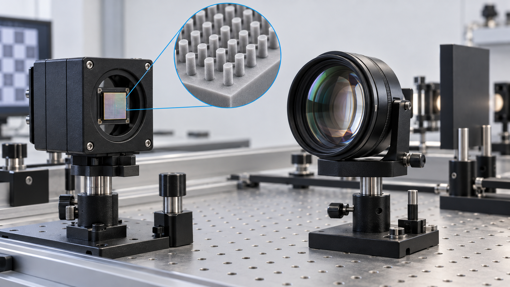
- Metalenses and flat optics (the short version)
- Principle — copying a lens's phase onto a flat surface
- How phase is made — delay by pillar width, or rotation by orientation
- A materials engineer's view 1: choose materials by refractive index, absorption and achievable height
- Our calculation: the number of elements, and the shift from chromatic aberration
- The wall of broadband operation — group delay, aperture and efficiency trade-offs
- Manufacturing — from electron-beam writing to semiconductor lithography and nanoimprint
- A materials engineer's view 2: what matters in volume production
- Where deployment stands — depth sensors, LiDAR, AR/VR
- Laboratory performance versus deployment
- Limits, and what could not be confirmed
- How to read evaluations and standards
- Glossary
- References (primary sources)
- Claim-to-source audit
Sourced = stated in published material (link given)
Our calculation = a figure this article derived, with the assumptions spelled out
Not yet confirmed = a plan, schedule or research-stage matter whose record has not been confirmed
Materials-design interpretations are marked separately as Commentary. Inference is shown in bold.
The efficiency, numerical-aperture and aperture figures here are laboratory results for particular wavelengths, polarisations and samples, or company announcements. The definition of efficiency (the share of light that lands in the focal spot, or the share of transmitted light) differs from paper to paper, so please do not rank values obtained under different conditions. A claim of being “the world’s first” and shipment counts are the claims of the announcing company, not independent confirmation. This article does not rank companies or products. Metamaterials for radio waves and sound are covered in the previous article (see our explainer on metamaterials and metasurfaces), and resonances in metal nanostructures in our explainer on plasmonics and nanophotonics; here we stay with their use as optical elements.
1. Metalenses and flat optics (the short version)
- Replace the lens’s “thickness” with the “dimensions of pillars”: an ordinary lens makes an optical path difference (a phase difference) through differences in glass thickness. A metalens makes phase through the width and orientation of sub-wavelength pillars on a flat substrate. The overview by Khorasaninejad and Capasso says metalenses are ultrathin, lightweight and flat, and, thanks to straightforward fabrication that generally needs a single lithography step and to the possibility of vertical integration, could replace or complement refractive and diffractive lensesSourced [Source 4]
- The difficulty is “a wide wavelength range” and “a large aperture”: at a single wavelength, a TiO2 metalens with a numerical aperture of 0.8 and focusing efficiency of 66–86% has been reportedSourced [Source 1]. Suppress chromatic aberration across the visible, however, and the reported efficiencies fall to roughly 20–50%, with fundamental limits tying aperture, numerical aperture and bandwidth togetherSourced [Sources 5, 6, 7, 8]
- Practical use starts with “single-wavelength near-infrared”: in 2022 STMicroelectronics announced the first use of a metasurface optic in a direct time-of-flight (dToF) sensor (a company announcement). A depth sensor uses essentially one near-infrared wavelength, which avoids the chromatic-aberration problemSourced [Sources 17, 18]
Whether a metalens is viable depends on “at what wavelength, over what aperture, and with what efficiency” it is used. For a single wavelength, small apertures and the near-infrared, products are on the market; broadband, large-aperture visible imaging remains a research problem that must be attacked with materials, design and computation together. Phrases such as “world first” or “comparable to conventional lenses” must always be read together with their conditions (wavelength, aperture, definition of efficiency).
2. Principle — copying a lens’s phase onto a flat surface
An ideal thin lens turns an incident plane wave into a spherical wave converging on the focus. The phase required, at distance r from the lens centre and for focal length f, has the form φ(r) = −(2π/λ)(√(r²+f²) − f) (λ is the wavelength; this is the general expression for converting to a spherical wave and is our commentary). An ordinary lens makes this phase by varying the glass thickness from centre to edge. A metalens makes the same phase through the dimensions of pillars arranged on a flat surface of constant thickness. Lin et al. patterned a 100 nm thick silicon layer into a dense arrangement of silicon nanobeam antennas and realised ultrathin gratings, lenses and axicons that reach high efficiency in transmission mode in the visible spectrum. They note that semiconductors offer easy integration with electronics and can be made with mature semiconductor fabrication technologiesSourced [Source 3].
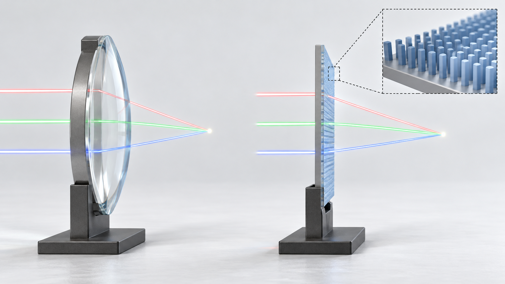
View the original SVG schematic and exact annotations
3. How phase is made — delay by pillar width, or rotation by orientation
There are two broad ways to make phase (the division below is our commentary).
| Method | Mechanism | Character | Reported example |
|---|---|---|---|
| Propagation phase | Change the pillar width or cross-section to change the delay of light passing through the pillar | The pillar can be treated as a short waveguide. Polarisation-independent designs are possible | Arbabi et al. used high-contrast dielectric elliptical nanoposts for complete control of polarisation and phase, with a measured efficiency of 72–97% depending on the designSourced [Source 2] |
| Geometric phase (rotation) | Rotate identical pillars place by place. With circularly polarised light, a phase set by the rotation angle is imparted | The phase is set by the rotation angle alone, independent of wavelength (Lee et al.). Many designs, however, use circular polarisation | The TiO2 metalens of Khorasaninejad et al. (NA 0.8) and the TiO2 nanofins of Chen et al. In Chen et al.’s measurements, crossed circular polarisers were used to reduce background lightSourced [Sources 1, 5, 14] |
Park et al. report that their all-glass metalens focuses at the diffraction limit for any homogeneously polarised incidence at visible wavelengths [Source 12]. Polarisation handling differs from design to design, so always check whether there is polarisation dependence.
In 2016, Khorasaninejad et al. made metalenses with a numerical aperture (NA) of 0.8 from high-aspect-ratio titanium dioxide (TiO2) metasurfaces. They showed diffraction-limited focusing at wavelengths of 405, 532 and 660 nm with efficiencies of 86, 73 and 66%, resolution of nanoscale features separated by subwavelength distances, magnification as high as 170×, and image quality comparable to a state-of-the-art commercial objectiveSourced [Source 1] (single-wavelength designs; the definition of efficiency depends on the paper). According to Chen et al., a TiO2 nanofin can be fabricated by electron-beam lithography followed by atomic layer deposition (ALD); in the same paper the lens elements had a height of 600 nm and a spacing of 400 nmSourced [Source 5]. ALD itself is covered in our explainer on atomic layer deposition.
4. A materials engineer’s view 1: choose materials by refractive index, absorption and achievable height
| Material | Reported wavelength range | How it was made (as reported) | Materials-side points (including commentary) |
|---|---|---|---|
| TiO2 | Visible (405–670 nm reported) | Electron-beam lithography and ALD (Chen et al.). High-aspect-ratio structures (Khorasaninejad et al.)Sourced [Sources 1, 5] | A representative high-index material with low absorption in the visible. The height that can be made sets the size of the group delay (Chapter 6) |
| Silicon nitride (SiN) | Visible (RGB imaging by Tseng et al.) | 705 nm of SiN deposited on a fused-silica wafer by plasma-enhanced CVD and patterned by electron-beam lithography (the method of Tseng et al.)Sourced [Source 16] | A standard thin film in semiconductor fabs. Its index is lower than that of TiO2, so taller pillars are needed for the same phase (our commentary) |
| Silicon (Si, a-Si) | Mainly near-infrared. Absorption appears in the visible | Lin et al.: nanobeams in a 100 nm Si layer. Lee et al.: Si nanorods made by nanoimprintSourced [Sources 3, 14] | Lee et al. state that silicon’s absorption is 1%, 8.2% and 21.4% at red, green and blue, that low-loss materials such as TiO2 or nitrides could greatly reduce it, and that they used silicon for its CMOS-compatible mass productionSourced [Source 14] |
| Gallium nitride (GaN) | The whole visible range (achromatic over 400–660 nm) | GaN-based resonant unit elements (Wang et al.)Sourced [Source 6] | One of the materials aimed at broadband achromatic operation. Substrate and deposition details were not confirmed here |
| Fused silica (all-glass) | Visible | 45 lenses of 1 cm diameter on a 4-inch fused-silica wafer by DUV projection stepper lithography (Park et al.)Sourced [Source 12] | Low absorption. But because the index is low, the etching is high-aspect-ratio (our commentary) |
| Resin plus a high-index thin film | Visible | A thin high-index film coated over a resin pattern made by nanoimprint (Kim et al.)Sourced [Source 13] | A route suited to volume production. Kim et al. state that the thin high-index film enhances light confinement and substantially raises conversion efficiency |
Wavelength ranges and methods are as stated in each paper. Because wavelength, NA, aperture and the definition of efficiency all differ, this table cannot be used to rank the materials in it.
The larger a pillar’s index difference from its surroundings (air or substrate), the less height it needs to make a large phase change. But high-index semiconductors absorb light at short wavelengths. The absorption Lee et al. show for silicon (21.4% at blue) is a concrete number for this relationshipSourced [Source 14]. In the visible, designs move to materials with a large bandgap that are transparent there, such as TiO2, SiN and GaN. In the near-infrared (850–940 nm), absorption becomes less of a problem even with silicon-based materials (our commentary). The other constraint is the height (aspect ratio) that can be fabricated. Chen et al. state that the group delay is the ratio of nanofin height to group velocity and is set by the nanofin dimensions and material, and they cite a TiO2 structure of about 4.5 µm height corresponding to a group delay of about 37 fsSourced [Source 5]. Metalens materials development is therefore asked for “transparent and high-index” together with “tall, thin, uniform, and over a large area” at the same time (our commentary).
5. Our calculation: the number of elements, and the shift from chromatic aberration
(1) The number of elements
Assume a pillar pitch of 400 nm on a square lattice, as in the element example of Chen et al.Sourced [Source 5]. A circle of 1 mm diameter holds about 4.9 million pillars, one of 1 cm about 490 million, and one of 2 cm about 2 billionOur calculation (circle area divided by the square of the pitch; the real pillar count varies with the design). Park et al. state that centimetre-scale metalenses may require up to billions of subwavelength structures, which can constrain size-scalability and mass productionSourced [Source 12]. She et al. cut the design file of a 1 cm diameter lens by three orders of magnitude with a layout compression algorithmSourced [Source 11].
(2) The shift from chromatic aberration
An ordinary metalens whose phase is matched at a single wavelength (a “diffractive metalens”) moves its focus as the wavelength changes. Chen et al. write the focal length as a power of frequency and state that a diffractive metalens has a focal-length shift whose focal length is proportional to frequency, similar to Fresnel lensesSourced [Source 5]. Written in wavelength, the focal length is inversely proportional to wavelength. With a design wavelength of 532 nm, the focal length is about 1.18 times as long at 450 nm and about 0.82 times at 650 nmOur calculation (focal length = focal length at the design wavelength × 532 nm / wavelength; paraxial approximation).
6. The wall of broadband operation — group delay, aperture and efficiency trade-offs
To make a lens achromatic, light of every wavelength must reach the focus at the same moment, so besides phase, the group delay (the delay of the travelling wave packet) and its wavelength dependence have to be designed pillar by pillar. Chen et al. designed nanofins that control phase, group delay and group delay dispersion together and showed diffraction-limited achromatic focusing and imaging from 470 to 670 nm. The metalens is a single layer of nanostructures of thickness on the order of the wavelength; its first design, with a numerical aperture of 0.2, has an efficiency of about 20% at 500 nmSourced [Source 5]. Wang et al. showed, with GaN-based resonant elements, an achromatic metalens whose focal length stays unchanged from 400 to 660 nm (about 49% bandwidth of the central wavelength), with NA 0.106 and an average efficiency of about 40% over the visibleSourced [Source 6]. Shrestha et al. showed dielectric metalenses with a near-constant focal length over 1200–1650 nm and polarisation-independent efficiency up to 50%, derived equations governing the trade-offs among lens diameter, numerical aperture and achromatic bandwidth, and state that the metalenses they demonstrated reach those fundamental limitationsSourced [Source 7].
Let us put numbers on this limit. Chen et al. state that the range of group delay required of an achromatic metalens is proportional to its radius and numerical aperture (R×NA/(2c) in the small-angle approximation)Sourced [Source 5]. Here we avoid the small-angle approximation and use geometry: the optical-path difference between edge and centre, divided by the speed of lightOur calculation. The range of delay required is about 3.7 fs for 220 µm diameter and NA 0.02, about 17 fs for 100 µm and NA 0.2, about 170 fs for 1 mm and NA 0.2, about 830 fs for 1 mm and NA 0.8, and about 1,700 fs for 1 cm and NA 0.2.
The delay grows roughly in proportion to aperture and numerical aperture. For the achromatic metalens of Chen et al. at 220 µm diameter and NA 0.02, the range required is about 3.7 fs, which fits within a 600 nm-tall element (about 5.5 fs). At 1 mm and NA 0.2, about 170 fs is needed, which even 4.5 µm of TiO2 (about 37 fs) cannot supplyOur calculation. Inference: this is probably one reason why reports of achromatic metalenses cluster at small apertures and low NA. Presutti and Monticone derived bandwidth limits for metalenses from the fact that the product of achievable time delay and bandwidth is limited in any time-invariant system, and showed that all metalenses designed thus far obey the boundSourced [Source 8].
Another route is to combine the optic with computation. Tseng et al. introduced “neural nano-optics”, which learns the metasurface structure together with a neural image-reconstruction algorithm; they report an order of magnitude lower reconstruction error than existing approaches, the widest field of view for full-colour metasurface operation, and the largest demonstrated aperture, 0.5 mm at an f-number of 2Sourced [Source 16]. Li et al. showed, by exploiting constructive interference of light from multiple zones and dispersion engineering, millimetre-scale-diameter, high-NA, submicron-thin metasurface lenses that focus the primary colours (red, green, blue) achromatically at the diffraction limit, and demonstrated a virtual-reality system based on a home-built fibre-scanning near-eye displaySourced [Source 15].
The definition of efficiency differs between papers. Chen et al. obtain efficiency by dividing the power in the focal spot by the power of the circularly polarised incident light passing through an aperture of the same diameter as the metalensSourced [Source 5]. Other papers may use the share of transmitted light, polarisation conversion efficiency or diffraction efficiency (our commentary). Engelberg et al. present a metric for the overall performance of a metalens and apply it to determine the optimal operating spectral rangeSourced [Source 10]. It shows that a commonly accepted evaluation metric has not yet settled (our commentary). There is debate over metalenses versus conventional diffractive lenses. Engelberg and Levy argue that metalenses do not replace diffractive optics but expand on it, and give their opinion on the debate over whether metalenses offer real advantages over diffractive lensesSourced [Source 9].
7. Manufacturing — from electron-beam writing to semiconductor lithography and nanoimprint
The challenge for metalenses is to arrange sub-wavelength pillars uniformly and cheaply over a centimetre-scale area (the calculation in Chapter 5). The reported manufacturing methods fall into three streams.
- 1 Electron-beam writing plus ALD: the TiO2 nanofins of Chen et al. were made by electron-beam lithography and atomic layer depositionSourced [Source 5]. The freedom in shape is high, but writing takes time, so it does not suit large apertures (our commentary)
- 2 Semiconductor exposure (steppers): She et al. took the view that semiconductor manufacturing technology, whose feature sizes were already denser than the wavelength of light by the mid-1990s, can make lenses. With a layout compression algorithm and stepper photolithography they imaged with a single near-infrared metalens of 2 cm diameter and under a micron in thickness, implementing the ideal thin-lens equationSourced [Source 11]. Park et al. made 45 metalenses of 1 cm diameter on a 4-inch fused-silica wafer by DUV projection stepper lithography and compared them, by Strehl ratio and modulation transfer function (MTF), with commercial spherical and aspherical singlet lenses of similar sizeSourced [Source 12]. These exposure technologies are covered in our explainer on lithography and EUV
- 3 Nanoimprint: Kim et al. made a master by DUV argon-fluoride (ArF) immersion lithography and replicated it by wafer-scale nanoimprint. From one 12-inch master stamp, hundreds of centimetre-scale metalenses can be fabricated, and coating a thin high-index film raises conversion efficiency substantially, they stateSourced [Source 13]. Lee et al. also showed full-colour imaging and the feasibility of mass production with a nanoimprinted large-area see-through metalensSourced [Source 14]. Nanoimprint itself is covered in our explainer on self-assembly and nanoimprint
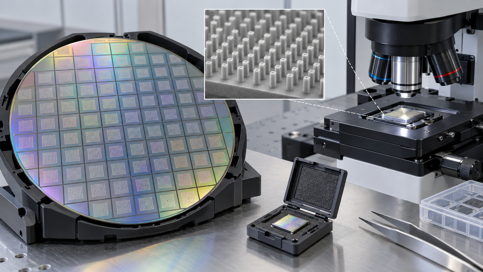
As a manufacturing record, Metalenz said in its announcement of 26 June 2023 that, with UMC (a Taiwanese semiconductor foundry with 12-inch fabs), it was releasing its supply chain for metasurface optics to mass production (a company announcement)Sourced [Source 19]. In its joint announcement of 10 July 2025, ST stated that using 300 mm wafers ensures high precision in optical applications along with the scalability and robustness of semiconductor manufacturing (a company’s description)Sourced [Source 18].
8. A materials engineer’s view 2: what matters in volume production
A metalens’s phase is set by pillar width, height, sidewall shape and refractive index. If dimensions drift by a few to a few tens of nanometres, the phase drifts, and the quality of the focal spot and the efficiency suffer (our commentary). Chen et al. measured about 20% efficiency around 500 nm against a theoretically predicted 50%, and say the deviation likely results from fabrication errors and coupling between neighbouring elements (the design treated each element in isolation with periodic boundary conditions and ignored near-field coupling)Sourced [Source 5]. Inference: fabricating high-aspect-ratio pillars across a whole wafer with uniform sidewall angle and height is likely to govern yield. Published primary sources gave no figures for the yield or dimensional tolerance of production items that we could confirm.
In the resin-plus-high-index-film approach, the moulding accuracy of the resin and the thickness uniformity of the thin high-index film directly set phase and efficiency. That Kim et al. state that the thin high-index film substantially raised conversion efficiencySourced [Source 13] implies that film thickness, index and adhesion have to be managed as material properties of a moulded lens (our commentary).
Temperature: ST states that replacing the lens stacks with metasurface optics improved the optical performance and temperature stability of the FlightSense modules and reduced their size and complexity (a company claim; the basis of comparison and figures are not given in the announcement)Sourced [Source 18]. How the thermal expansion and temperature dependence of the refractive index of the pillar material (fused silica, silicon and so on) affect focal stability could not be confirmed in primary sources.
9. Where deployment stands — depth sensors, LiDAR, AR/VR
Practical examples begin with uses that employ a single near-infrared wavelength. A depth sensor (direct time-of-flight sensor, dToF) uses a laser of one near-infrared wavelength and measures the time for light to return, so it avoids the chromatic-aberration problem (our commentary). In its announcement of 9 June 2022, STMicroelectronics said that the VL53L8 dToF sensor is the market debut of meta-optics devices developed through its partnership with Metalenz. The announcement says that the meta-optics replace some of the existing optics and bring performance, power, size and cost advantages (a company announcement)Sourced [Source 17]. ST’s remark that the initial target is applications using near-infrared wavelengths also supports the point that it starts from near-infrared single wavelengthsSourced [Source 17].
| Use | What was published (as stated by the companies and institutions) | Conditions to keep in mind |
|---|---|---|
| dToF depth sensors (smartphones and others) | 9 June 2022: ST’s VL53L8 is the first market debut of meta-optics devices. Manufactured on silicon wafers alongside electronics in ST’s semiconductor front-end fabs. 10 July 2025: ST says that since 2022 it has shipped well over 140 million metasurface optics and FlightSense modules that use Metalenz IP | A company claim. The shipment count covers optics and modules combined, not meta-optics alone. Which part (transmit or receive side, focusing or diffusing) was replaced by meta-optics is not given in the announcementSourced [17, 18] |
| 3D-sensing supply chain (12-inch foundry) | 26 June 2023: Metalenz and UMC release a supply chain for metasurface optics to mass production. The first designs are for Dilusense | A company announcement. Scale and yield of production cannot be confirmedSourced [19] |
| Face authentication (polarisation meta-optics) | 26 February 2024: Metalenz announces that it chose Samsung’s ISOCELL Vizion 931 (a near-infrared global-shutter image sensor) for Polar ID. It says a human face’s polarisation signature allows authentication from a single image, with a 50% size and cost reduction over traditional face-unlock solutions. Several leading smartphone OEMs were said to be evaluating it at an early stage | A company claim, not an independent measurement. Inclusion in a product could not be confirmed hereSourced / Not yet confirmed [20] |
| LiDAR beam steering | Lumotive lists the LM10 (a Light Control Metasurface chip) as a solid-state optical beamforming semiconductor with no moving parts. Native field of view up to 160°, wavelengths 905 nm and 940 nm, active aperture 11 x 9 mm, compatible with VCSEL and edge-emitting lasers. It says that sub-wavelength nanostructures shape and steer light, and that the chips are manufactured with conventional silicon fabrication processes | The manufacturer’s stated values (product page). Measurement conditions and independent evaluation could not be confirmed. This is not an imaging lens but an element that changes beam direction electricallySourced [21] |
| AR/VR | Lee et al.: a nanoimprinted see-through metalens gives full-colour imaging with a wide field of view. Li et al.: a VR system demonstrated with a red-green-blue achromatic metalens. Kim et al.: an ultrathin VR device demonstrated with stamp-made metalenses | Laboratory demonstrations. Lee et al. note low cross-polarised efficiency (measured 12% red, 9% green, 2.5% blue) and room for improvementSourced [13, 14, 15] |
Examples are growing in which meta-optics creates the value of a system together with the sensor and computation, as in Polar ID. The neural nano-optics of Tseng et al. is likewise a design in which quality comes from image reconstruction together with the optic, not from the optical element aloneSourced [Source 16]. Seeing metalenses only as a “substitute for an ordinary lens” misses this direction (our commentary).
10. Laboratory performance versus deployment
| Aspect | Shown in laboratory or demonstration | What deployment asks | Source and label |
|---|---|---|---|
| Wavelength | Efficiency of 66–86% at single wavelengths (405, 532, 660 nm). Visible-wide achromatic operation at roughly 20–40% efficiency | Products start with single-wavelength near-infrared (dToF). Broadband visible imaging is immature | [1] [5] [6] [17] Sourced |
| Aperture and NA | Achromatic lenses at 220 µm diameter and NA 0.02, or small apertures at NA 0.2. Single-wavelength lenses at millimetre to centimetre scale | Whether lenses of smartphone-camera aperture can be made broadband. The required group delay scales with aperture and NA (Fig. 4) | [5] [12] [16] Sourced; group delay is Our calculation |
| Definition of efficiency | Differs by paper (focal-spot power divided by incident power through the same aperture, and others) | The lack of an index that lets values be compared under one definition. Standardised evaluation is still to come | [5] [10] Sourced |
| Field of view | The achromatic metalens of Chen et al. keeps a Strehl ratio above 0.8 to an incidence angle of about 15°, with a 30° imaging field of view | Whether a single-layer metasurface can hold aberrations across a wide field and the full frame; it has to be compared with the field of view of a real camera | [5] Sourced |
| Polarisation | Designs that use circular polarisation and polarisation-independent designs both exist | Whether performance holds for the polarisation of the real light source and application (unpolarised or linear) | [2] [5] [12] Sourced |
| Scale of fabrication | From small-aperture electron-beam writing to 45 lenses on a 4-inch wafer by stepper, to hundreds from a 12-inch master | Dimensional scatter, yield and cost. Published figures could not be confirmed | [5] [12] [13] Sourced; yield is Not yet confirmed |
| Company claims | Better optical performance and temperature stability, smaller size, a 50% reduction in size and cost for face authentication | The conditions of comparison (the other optical system, wavelength, temperature range, evaluation method) are not given in the announcements | [18] [20] Sourced (company claims) |
| Comparison with conventional diffractive lenses | A commentary that metalenses expand on diffractive optics | Telling apart what “only a metalens can do” (polarisation control, multifunction, volume production in semiconductor fabs) from uses a diffractive lens suffices for | [9] Sourced (a commentary) |
11. Limits, and what could not be confirmed
(1) Optical performance figures of products
The efficiency, resolution, field of view, temperature characteristics and yield of the products of ST, Metalenz and Lumotive could not be confirmed numerically from the announcements. Because the conditions of comparison could not be confirmed, the companies’ “advantages” are quoted as they stand.
(2) The definition of efficiency
We did not check the definition of efficiency used by Khorasaninejad et al. (Chen et al.’s definition was checked in the authors’ accepted manuscript). Values under different definitions are not ranked.
(3) The texts of papers
For Chen et al. we read the text in the authors’ accepted manuscript (Harvard DASH). For the other papers we relied on abstracts (OpenAlex, Semantic Scholar, the publishers’ pages) and whatever text could be checked. The pillar height and material properties in Khorasaninejad et al., the GaN deposition in Wang et al., and the material in Li et al. were not checked here.
(4) The texts of standards
We have not checked the texts (which are paid) of the ISO, JIS and IEC standards. Test procedures, conditions and pass criteria are not described.
(5) Other applications
Flat optics other than metalenses (diffractive optical elements, liquid-crystal lenses), infrared, ultraviolet and terahertz metalenses, metasurface devices other than metalenses (polarisation elements, holograms), and AR-glass waveguides are not covered here. Electromagnetic and acoustic waves are in the previous article (see our explainer on metamaterials and metasurfaces), and LiDAR on the optical-communications side is in our LiDAR explainer.
- A metalens is a flat plate that makes phase through pillar dimensions rather than thickness. At a single wavelength, TiO2 gives NA 0.8 and 66–86% efficiency (laboratory). Make it achromatic and the reported efficiencies fall to roughly 20–50%Sourced
- The limit is the product of group delay, aperture, NA and bandwidth. The delay required for achromatic operation is about 170 fs at 1 mm diameter and NA 0.2, which even 4.5 µm of TiO2 (about 37 fs) cannot supply, by our calculationOur calculation
- Materials must be transparent in the visible, high in index, and capable of being made tall and uniform. Silicon absorbs 21.4% at blue, and there is a move toward TiO2, SiN, GaN and the likeSourced
- Manufacturing is moving from electron-beam writing to semiconductor lithography and nanoimprint. Reports include 45 lenses of 1 cm diameter on a 4-inch wafer and hundreds from a 12-inch masterSourced
- Practical use starts with single-wavelength near-infrared. ST announced the first use in a dToF sensor in 2022 and in 2025 mentioned more than 140 million units shipped (optics and modules together; a company claim)Sourced
- Evaluation standards are scattered. We could not confirm an international standard specific to metalenses; the existing standards for OTF, MTF, camera resolution and diffraction efficiency are read with their conditionsSourced
12. How to read evaluations and standards
What is measured: the performance of a metalens is expressed by focal length, the size of the focal spot (whether it is diffraction-limited), the Strehl ratio, the MTF (the transfer of contrast at each spatial frequency), efficiency, the focus shift with wavelength (chromatic aberration), dependence on polarisation and angle of incidence, and field of view. In practice, Chen et al. recorded the point-spread function by stepping through the neighbourhood of the focal plane 1 µm at a time with a tunable laser and a microscope to find the focal length at each wavelengthSourced [Source 5]. Park et al. compared their lenses with commercial spherical and aspherical singlet lenses of similar size by Strehl ratio and MTFSourced [Source 12]. We found no ISO, IEC or IEEE standard that names metalenses. Existing optics standards, for photographic lenses, the optical transfer function, camera resolution, and the diffraction efficiency of holograms, are therefore applied with their conditionsSourced (a statement of what could not be confirmed).
| Item evaluated | ISO | IEC / IEEE | JIS | ASTM | What changes the value with measurement conditions |
|---|---|---|---|---|---|
| Focal length, effective aperture, f-numberSourced | Could not be confirmed | Could not be confirmed | JIS B 7094 (Japanese title: photographic lenses, method of measuring focal length; our translation) and JIS B 7095 (Japanese title: photographic lenses, method of measuring effective aperture, f-number and aperture ratio; our translation). The years of the editions and the correspondence to international standards were not checked [27, 28] | Could not be confirmed | Measurement wavelength (a diffractive metalens’s focal length varies inversely with wavelength, Fig. 3), polarisation, reference plane |
| Optical transfer function (OTF, MTF)Sourced | ISO 9334:2012 (Optics and photonics – Optical transfer function – Definitions and mathematical relationships). Edition 3, October 2012, confirmed in 2022. ISO 9335:2025 (same series – Principles and procedures of measurement). Edition 3, February 2025; interferometer-based instruments are outside its scope. ISO 15529:2010 (same series – Principles of measurement of modulation transfer function (MTF) of sampled imaging systems). Edition 3, August 2010, confirmed in 2025 [22, 23, 24] | Could not be confirmed | We could not confirm a JIS standard on the optical transfer function in the JIS search | Could not be confirmed | Measurement wavelength (single or broadband), field angle, polarisation, spatial frequency, source spectrum. For a lens used over a wide wavelength range, MTFs measured under different wavelength conditions cannot be compared (our commentary) |
| Camera resolution and spatial frequency response (SFR)Sourced | ISO 12233:2024 (Digital cameras – Resolution and spatial frequency responses). Edition 5, September 2024, replacing ISO 12233:2023 [25] | Could not be confirmed | Could not be confirmed | Could not be confirmed | A measurement of the whole camera, including lens, sensor and image processing, not of the lens alone. For imaging that includes computation (such as neural nano-optics), it needs to be confirmed how much is within the object of evaluation (our commentary) |
| Diffraction efficiencySourced | ISO 17901-1:2015 (Optics and photonics – Holography – Part 1: Methods of measuring diffraction efficiency and associated optical characteristics of holograms). Edition 1, July 2015, confirmed in 2025. Applies to holograms with a simple diffraction pattern [26] | Could not be confirmed | JIS Z 8791 (Japanese title: methods of measuring diffraction efficiency and associated optical characteristics of holograms; our translation). The year of the edition and the correspondence to the ISO standard were not checked [29] | Could not be confirmed | This is a standard for holograms; whether it can be used as it is for a metalens’s “focusing efficiency” was not checked here. Always confirm the definition of efficiency (focal spot, transmitted light or diffracted light) |
| Laser-source safety (dToF, LiDAR and other modules)Sourced | Could not be confirmed | IEC 60825-1:2014 (Safety of laser products – Part 1: Equipment classification and requirements). Edition 3.0, published 15 May 2014, stability date 2027. Whether it is the latest edition was not checked [30] | JIS C 6802 (Japanese title: safety of laser products, classification and requirements; our translation). The year of the edition and the correspondence to the IEC standard were not checked [31] | Could not be confirmed | Not a standard for the optical performance of a lens but a classification of the safety of light sources and modules. If meta-optics changes how the light spreads, the conditions for assessing the classification may change (our inference, not checked) |
| Evaluation specific to metalenses and metasurfacesSourced | Could not be confirmed | Could not be confirmed | Could not be confirmed | Could not be confirmed | Within what we searched, we found no ISO, IEC or IEEE standard that defines the efficiency or performance of metalenses. Papers use their own metrics (Engelberg et al. [Source 10]) and measurement methods (a statement of what could not be confirmed) |
Which standard we match to which item is our own arrangement (Our calculation). Numbers and titles were checked on the official ISO page for ISO, the IEC Webstore for IEC, and the JISC JIS search for JIS. We did not find an ASTM standard corresponding to the evaluation of metalenses and flat optics, and did not open the ASTM website.
How the standards differ in standing
- ISO and IEC are international standards; JIS is Japan’s national standard. Whether JIS B 7094, B 7095, Z 8791 and C 6802 are identical to particular ISO or IEC standards was not checked here
- Most standards in this field are “general test methods for optical systems”, not for metalenses. Because we could not confirm an international standard specific to metalenses, each paper’s own measurement method and metric are used [5, 10, 12]
- ASTM: we could not confirm an ASTM standard corresponding to the evaluation of metalenses and flat optics
Cautions in reading the standards
- A standard is a test method, not a guarantee of performance. ISO 9335 is guidance on constructing and using OTF measuring equipment and excludes interferometer-based instruments [23]. If the measurement approach differs, the same MTF number can mean different conditions
- The same named property can differ in definition and conditions. “Efficiency” is the focal-spot power divided by the incident power through the same aperture (Chen et al.), and other papers use other definitions [5]. Always read an efficiency figure together with its definition, wavelength, polarisation and aperture
- A camera standard measures the whole system. ISO 12233 is a method for camera resolution and SFR [25]; it does not separate out the lens alone or the “lens share” of imaging that includes computation (our commentary)
- Read a manufacturer’s value together with the standard, edition and test conditions it follows. ST’s “improved optical performance and temperature stability” gives no basis of comparison in the announcement [18]. Lumotive’s field of view and wavelengths are the manufacturer’s stated values on its product page [21]
- The gap between a standard’s range and conditions of use: an MTF or efficiency measured at a single wavelength does not show the performance of a real device over a wide wavelength range, a wide field and changing temperature
13. Glossary
- Metalens
- A flat lens made from a metasurface.
- Nanopillar (nanopost, nanofin)
- A pillar smaller than the wavelength. Its width or orientation sets the phase.
- Propagation phase
- Phase made by changing the pillar’s width or shape to change the delay of light passing through it.
- Geometric phase
- Phase imparted to circularly polarised light by rotating identical pillars.
- NA (numerical aperture)
- A value expressing the angular range over which a lens gathers light.
- Chromatic aberration
- The shift of the focus position with wavelength.
- Group delay
- The delay of a wave packet passing through an element. Achromatic operation needs its wavelength dependence designed.
- Strehl ratio
- The ratio of the peak intensity of the real focal spot to that of an ideal diffraction-limited spot.
- MTF / OTF
- The optical transfer function: how much image contrast is preserved at each spatial frequency.
- ALD
- Atomic layer deposition: growing a thin film one layer at a time.
- dToF
- Direct time of flight: a distance sensor that measures the round-trip time of light directly.
- Nanoimprint
- Replicating a fine pattern by pressing a mould (stamp) into resin.
14. References (primary sources)
- Khorasaninejad M. et al. “Metalenses at visible wavelengths: Diffraction-limited focusing and subwavelength resolution imaging”, Science 352, 1190–1194 (2016), DOI 10.1126/science.aaf6644 — doi.org/10.1126/science.aaf6644
- Arbabi A. et al. “Dielectric metasurfaces for complete control of phase and polarization with subwavelength spatial resolution and high transmission”, Nat. Nanotechnol. 10, 937–943 (2015), DOI 10.1038/nnano.2015.186 — doi.org/10.1038/nnano.2015.186
- Lin D. et al. “Dielectric gradient metasurface optical elements”, Science 345, 298–302 (2014), DOI 10.1126/science.1253213 — doi.org/10.1126/science.1253213
- Khorasaninejad M., Capasso F. “Metalenses: Versatile multifunctional photonic components”, Science 358, eaam8100 (2017), DOI 10.1126/science.aam8100 — doi.org/10.1126/science.aam8100
- Chen W. T. et al. “A broadband achromatic metalens for focusing and imaging in the visible”, Nat. Nanotechnol. 13, 220–226 (2018), DOI 10.1038/s41565-017-0034-6 (the text was checked in the authors’ accepted manuscript, Harvard DASH) — doi.org/10.1038/s41565-017-0034-6
- Wang S. et al. “A broadband achromatic metalens in the visible”, Nat. Nanotechnol. 13, 227–232 (2018), DOI 10.1038/s41565-017-0052-4 — doi.org/10.1038/s41565-017-0052-4
- Shrestha S. et al. “Broadband achromatic dielectric metalenses”, Light: Science & Applications 7, 85 (2018), DOI 10.1038/s41377-018-0078-x — doi.org/10.1038/s41377-018-0078-x
- Presutti F., Monticone F. “Focusing on bandwidth: achromatic metalens limits”, Optica 7, 624–631 (2020), DOI 10.1364/OPTICA.389404 — doi.org/10.1364/OPTICA.389404
- Engelberg J., Levy U. “The advantages of metalenses over diffractive lenses”, Nat. Commun. 11, 1991 (2020), DOI 10.1038/s41467-020-15972-9 (a commentary) — doi.org/10.1038/s41467-020-15972-9
- Engelberg J. et al. “How good is your metalens? Experimental verification of metalens performance criterion”, Opt. Lett. 45, 3869 (2020), DOI 10.1364/ol.394680 — doi.org/10.1364/ol.394680
- She A. et al. “Large area metalenses: design, characterization, and mass manufacturing”, Opt. Express 26, 1573–1585 (2018), DOI 10.1364/OE.26.001573 — doi.org/10.1364/OE.26.001573
- Park J.-S. et al. “All-Glass, Large Metalens at Visible Wavelength Using Deep-Ultraviolet Projection Lithography”, Nano Lett. 19, 8673–8682 (2019), DOI 10.1021/acs.nanolett.9b03333 — doi.org/10.1021/acs.nanolett.9b03333
- Kim J. et al. “Scalable manufacturing of high-index atomic layer–polymer hybrid metasurfaces for metaphotonics in the visible”, Nat. Mater. 22, 474–481 (2023), DOI 10.1038/s41563-023-01485-5 — doi.org/10.1038/s41563-023-01485-5
- Lee G.-Y. et al. “Metasurface eyepiece for augmented reality”, Nat. Commun. 9, 4562 (2018), DOI 10.1038/s41467-018-07011-5 — doi.org/10.1038/s41467-018-07011-5
- Li Z. et al. “Meta-optics achieves RGB-achromatic focusing for virtual reality”, Sci. Adv. 7, eabe4458 (2021), DOI 10.1126/sciadv.abe4458 — doi.org/10.1126/sciadv.abe4458
- Tseng E. et al. “Neural nano-optics for high-quality thin lens imaging”, Nat. Commun. 12, 6493 (2021), DOI 10.1038/s41467-021-26443-0 — doi.org/10.1038/s41467-021-26443-0
- Metalenz and STMicroelectronics “Metalenz and STMicroelectronics Deliver World’s First Optical Metasurface Technology for Consumer Electronics Devices” (9 June 2022; company announcement) — metalenz.com (announcement of 9 June 2022)
- STMicroelectronics and Metalenz “STMicroelectronics and Metalenz Sign a New License Agreement to Accelerate Metasurface Optics Adoption” (10 July 2025; company announcement) — metalenz.com (announcement of 10 July 2025)
- Metalenz “Metalenz Launches its Metasurface Optics on the Open Market in Partnership with UMC” (26 June 2023; company announcement) — metalenz.com (announcement of 26 June 2023)
- Metalenz “Metalenz Confirms Samsung ISOCELL Vizion Image Sensor as Light-Engine for Polar ID” (26 February 2024; company announcement) — metalenz.com (announcement of 26 February 2024)
- Lumotive “LM10” (product page for the LCM chip; manufacturer’s stated values) — lumotive.com/lm10
- ISO “ISO 9334:2012” page — iso.org/standard/57563.html
- ISO “ISO 9335:2025” page — iso.org/standard/85989.html
- ISO “ISO 15529:2010” page — iso.org/standard/56069.html
- ISO “ISO 12233:2024” page — iso.org/standard/88626.html
- ISO “ISO 17901-1:2015” page — iso.org/standard/60946.html
- Japanese Industrial Standards Committee (JISC) JIS search listing for “JIS B 7094” — jisc.go.jp (JIS B 7094)
- Japanese Industrial Standards Committee (JISC) JIS search listing for “JIS B 7095” — jisc.go.jp (JIS B 7095)
- Japanese Industrial Standards Committee (JISC) JIS search listing for “JIS Z 8791” — jisc.go.jp (JIS Z 8791)
- IEC “IEC 60825-1:2014” product page (IEC Webstore) — webstore.iec.ch/en/publication/3587
- Japanese Industrial Standards Committee (JISC) JIS search listing for “JIS C 6802” — jisc.go.jp (JIS C 6802)
15. Claim-to-source audit
| Claim in the text | Basis | Label |
|---|---|---|
| A TiO2 metalens, NA 0.8, wavelengths 405, 532 and 660 nm, efficiencies of 86, 73 and 66%, magnification up to 170x | Khorasaninejad et al. (2016) Reference 1 https://doi.org/10.1126/science.aaf6644 | Sourced |
| High-contrast dielectric elliptical nanoposts, complete control of polarisation and phase, measured efficiency 72–97% | Arbabi et al. (2015) Reference 2 https://doi.org/10.1038/nnano.2015.186 | Sourced |
| Nanobeams in a 100 nm Si layer, transmission-mode gratings, lenses and axicons in the visible, the advantages of semiconductors | Lin et al. (2014) Reference 3 https://doi.org/10.1126/science.1253213 | Sourced |
| Metalenses are ultrathin, lightweight and flat, with a single lithography step and vertical integration, and could replace or complement refractive and diffractive lenses | Overview by Khorasaninejad and Capasso (2017) Reference 4 https://doi.org/10.1126/science.aam8100 | Sourced |
| Achromatic operation over 470–670 nm, NA 0.2, efficiency about 20% (500 nm; prediction 50%), 220 µm diameter at NA 0.02, about 40% for small-diameter lenses, TiO2 nanofins (600 nm tall, 400 nm spacing, electron-beam lithography and ALD), focal length as a power of frequency, group-delay range R x NA/(2c), about 37 fs for 4.5 µm of TiO2, 22 fs being about four times what 600 nm height gives, the efficiency measurement method, 30° field of view and Strehl ratio above 0.8 to about 15°, fabrication errors and inter-element coupling | Chen et al. (2018); text checked in the authors’ accepted manuscript Reference 5 https://doi.org/10.1038/s41565-017-0034-6 | Sourced |
| GaN resonant elements, achromatic over 400–660 nm (about 49% bandwidth), NA 0.106, average efficiency about 40% | Wang et al. (2018) Reference 6 https://doi.org/10.1038/s41565-017-0052-4 | Sourced |
| Dielectric achromatic metalenses over 1200–1650 nm, polarisation-independent, efficiency up to 50%, equations relating diameter, NA and bandwidth, reaching the limits | Shrestha et al. (2018) Reference 7 https://doi.org/10.1038/s41377-018-0078-x | Sourced |
| Bandwidth limits for achromatic metalenses from the bound on the product of time delay and bandwidth; that existing metalenses obey the limit | Presutti and Monticone (2020) Reference 8 https://doi.org/10.1364/OPTICA.389404 | Sourced |
| A commentary that metalenses expand on rather than replace diffractive optics, and on the debate over advantages versus diffractive lenses | Engelberg and Levy (2020) Reference 9 https://doi.org/10.1038/s41467-020-15972-9 | Sourced |
| A proposed metric for the overall performance of metalenses and its application to the optimal operating spectral range | Engelberg et al. (2020) Reference 10 https://doi.org/10.1364/ol.394680 | Sourced |
| Layout compression (three orders of magnitude for 1 cm), a 2 cm, under-1-µm near-infrared metalens by stepper, the idea of making lenses with semiconductor manufacturing technology | She et al. (2018) Reference 11 https://doi.org/10.1364/OE.26.001573 | Sourced |
| An all-glass metalens of 1 cm diameter, 45 on a 4-inch fused-silica wafer, DUV projection stepper, comparison with commercial lenses by Strehl ratio and MTF, billions of structures at centimetre scale | Park et al. (2019) Reference 12 https://doi.org/10.1021/acs.nanolett.9b03333 | Sourced |
| ArF immersion lithography with wafer-scale nanoimprint, a 12-inch master, hundreds of cm-scale metalenses, a substantial rise in conversion efficiency with a thin high-index film, a VR demonstration | Kim et al. (2023) Reference 13 https://doi.org/10.1038/s41563-023-01485-5 | Sourced |
| A nanoimprinted large-area see-through metalens, silicon’s absorption (red 1%, green 8.2%, blue 21.4%), the expectation of low-loss materials (TiO2, SiN), geometric phase independent of wavelength, measured cross-polarised efficiency (red 12%, green 9%, blue 2.5%) | Lee et al. (2018) Reference 14 https://doi.org/10.1038/s41467-018-07011-5 | Sourced |
| Red-green-blue achromatic metalenses, millimetre-scale aperture, high NA, submicron thickness, a VR system | Li et al. (2021) Reference 15 https://doi.org/10.1126/sciadv.abe4458 | Sourced |
| Neural nano-optics, an order of magnitude lower reconstruction error, 0.5 mm aperture at f/2, 705 nm of SiN deposited by PECVD | Tseng et al. (2021) Reference 16 https://doi.org/10.1038/s41467-021-26443-0 | Sourced |
| The first use of meta-optics in ST’s VL53L8 dToF sensor (9 June 2022), replacement of some existing optics, manufacture on silicon wafers in ST’s front-end fabs, initial focus on near-infrared | Joint announcement by Metalenz and ST (company announcement) Reference 17 https://metalenz.com/metalenz-and-stmicroelectronics-deliver-worlds-first-optical-metasurface-technology-for-consumer-electronics-devices/ | Sourced |
| More than 140 million units shipped since 2022 (metasurface optics and FlightSense modules), 300 mm wafer processes, improved optical performance and temperature stability and reduced size and complexity (the company’s statement) | Joint announcement by ST and Metalenz (10 July 2025) Reference 18 https://metalenz.com/stmicroelectronics-and-metalenz-sign-a-new-license-agreement-to-accelerate-metasurface-optics-adoption/ | Sourced |
| Metalenz and UMC (12-inch fabs) releasing the supply chain to mass production, with Dilusense as the first design (26 June 2023) | Metalenz announcement (company announcement) Reference 19 https://metalenz.com/metalenz-launches-its-metasurface-optics-on-the-open-market-in-partnership-with-umc/ | Sourced |
| The company’s statements on Polar ID (choice of Samsung’s ISOCELL Vizion 931, authentication from a single image, 50% size and cost reduction, early evaluation by several OEMs) (26 February 2024) | Metalenz announcement (company announcement) Reference 20 https://metalenz.com/metalenz-confirms-samsung-isocell-vizion-image-sensor-as-light-engine-for-polar-id-the-worlds-smallest-most-affordable-and-secure-face-unlock-solution/ | Sourced / Not yet confirmed |
| Lumotive LM10: beamforming without moving parts, native field of view up to 160°, 905 and 940 nm, active aperture 11 x 9 mm, VCSEL and EEL compatibility (manufacturer’s stated values) | Lumotive product page Reference 21 https://www.lumotive.com/lm10/ | Sourced |
| Number, title and edition: ISO 9334:2012 (Edition 3, October 2012, confirmed 2022) | ISO Reference 22 https://www.iso.org/standard/57563.html | Sourced |
| Number, title and edition: ISO 9335:2025 (Edition 3, February 2025; interferometer-based instruments outside its scope) | ISO Reference 23 https://www.iso.org/standard/85989.html | Sourced |
| Number, title and edition: ISO 15529:2010 (Edition 3, August 2010, confirmed 2025) | ISO Reference 24 https://www.iso.org/standard/56069.html | Sourced |
| Number, title and edition: ISO 12233:2024 (Edition 5, September 2024, replacing ISO 12233:2023) | ISO Reference 25 https://www.iso.org/standard/88626.html | Sourced |
| Number, title and edition: ISO 17901-1:2015 (Edition 1, July 2015, confirmed 2025; holograms with a simple diffraction pattern) | ISO Reference 26 https://www.iso.org/standard/60946.html | Sourced |
| Number and title: JIS B 7094 (Japanese title on the JISC listing) | JISC JIS search Reference 27 https://www.jisc.go.jp/app/jis/general/GnrJISNumberNameSearchList?show&jisStdNo=B7094 | Sourced |
| Number and title: JIS B 7095 (Japanese title on the JISC listing) | JISC JIS search Reference 28 https://www.jisc.go.jp/app/jis/general/GnrJISNumberNameSearchList?show&jisStdNo=B7095 | Sourced |
| Number and title: JIS Z 8791 (Japanese title on the JISC listing) | JISC JIS search Reference 29 https://www.jisc.go.jp/app/jis/general/GnrJISNumberNameSearchList?show&jisStdNo=Z8791 | Sourced |
| Number, title and edition: IEC 60825-1:2014 (Edition 3.0, 15 May 2014, stability date 2027) | IEC Webstore Reference 30 https://webstore.iec.ch/en/publication/3587 | Sourced |
| Number and title: JIS C 6802 (Japanese title on the JISC listing) | JISC JIS search Reference 31 https://www.jisc.go.jp/app/jis/general/GnrJISNumberNameSearchList?show&jisStdNo=C6802 | Sourced |
| The number of pillars (1 mm diameter: about 4.9 million; 1 cm: about 490 million; 2 cm: about 2 billion; on an assumed 400 nm square lattice), chromatic aberration (for a 532 nm design, about 1.18x at 450 nm and about 0.82x at 650 nm), the delay range required for achromatic operation (about 3.7, 17, 170, 830 and 1,700 fs), and the back-calculated delay of a 600 nm-tall element (about 5.5 fs) | Our calculation. The pillar count assumes a 400 nm pitch, chromatic aberration is a paraxial approximation, and the required delay is edge-to-centre path difference divided by the speed of light (in air, ideal thin lens). About 5.5 fs is back-calculated from the statement of Chen et al. that 22 fs is about four times what 600 nm height gives | Our calculation |
| The definition of efficiency used by Khorasaninejad et al. and their pillar height and material properties, the GaN deposition in Wang et al., the material in Li et al., efficiency, resolution, field of view, temperature characteristics and yield of products, international standards specific to metalenses, and the texts of standards | Not given, because they could not be confirmed in the primary sources accessible to this investigation | Commentary |
| The readings “single-wavelength near-infrared (dToF) avoids chromatic aberration”, “designs move to transparent high-index materials in the visible”, “dimensional scatter becomes phase error”, “yield governs volume production”, “the required delay is a background to reports clustering at small apertures”, “the field-of-view limit of a single-layer metasurface”, and “the direction of creating value as a system”. The phase formula and the two-way classification of how phase is made | Our own arrangement and commentary based on the published material; not views expressed by the companies or institutions | Commentary |
| That Figs. 2, 3, 4 and 5 are explanatory drawings, not real data, and that Figs. 1 and 6 are AI-generated images | Note from this article | Commentary |
Last updated 10 October 2026. Sources are limited to primary material (peer-reviewed papers, official pages of ISO, IEC and JISC, and company announcements). The texts of standards are paid and could not be checked. The ASTM International website was not opened. Because the article includes structural readings and materials-design interpretations, those are marked as Commentary and kept separate from sourced fact. The efficiency, resolution, field of view, temperature characteristics and yield of products, international standards specific to metalenses, and the texts of standards could not be confirmed and are not stated here. Figures from announcements are the stated values of the companies and institutions that made them, and are not meant for ranking experiments that differ in conditions. All figures are explanatory concept graphics. Figs. 2, 3, 4 and 5 are vector drawings; Figs. 1 and 6 are AI-generated images, and none of them shows a real photograph, measured data or a physical product.