TECHNOLOGY EXPLAINER
Spintronic Materials
— materials that use the electron’s spin as well as its charge are decided by a few nanometres at the interface
An electron has charge, and also a property as a tiny magnet, its spin. Spintronics is the technology of reading, writing and carrying that spin. Hard-disk read heads and automotive magnetic sensors are already widespread, and magnetic memory (MRAM) is a product in embedded applications. What decides their performance is less the circuit design than the materials and interfaces of a stack of thin films a few nanometres thick. This article sets out, within the range of primary sources, magnetoresistance (GMR and TMR), the device materials of MRAM (STT and SOT), materials that generate spin current, Heusler alloys, and skyrmions, antiferromagnets and two-dimensional magnets. MRAM products and mass production are left to the “Nanomemory” article of this series; here the subject is seen from the materials side.
- What spintronic materials are (the short version)
- What spin is used for — reading, writing and carrying
- Magnetoresistance materials — from GMR to MgO-based TMR
- Device materials for MRAM — STT and SOT, thermal stability and scaling
- Materials that generate spin current — heavy metals and their resistivity
- Heusler alloys — the hope of half-metals, and the wall of temperature
- New material classes — skyrmions, antiferromagnets, two-dimensional magnets
- Walls of materials and process — will it fit on a 300 mm wafer?
- Limits, and what could not be confirmed
- How to read evaluations and standards
- Glossary
- References (primary sources)
- Claim-to-source audit
Sourced = stated in published material (link given)
Our calculation = a figure this article derived, with the assumptions spelled out
Not yet confirmed = a standard still being drafted, a research-stage concept, or a target of companies or researchers whose record has not been confirmed
Materials-design interpretations are marked separately as Commentary. Inference is shown in bold.
Magnetoresistance numbers change greatly with measurement temperature (room or low), sample form (single crystal, polycrystal, thin film), annealing temperature, bias voltage and the definition of the TMR ratio. This article gives the temperature and conditions alongside each value. A laboratory maximum is not the value of a production device or of a cell inside an integrated circuit. Values under different conditions set side by side do not show which is better or which is easier to manufacture, and prices, market sizes and price forecasts are not covered. Note that the review by Dieny et al. is the accepted version of 2020. Progress since 2020 has not been checked within the scope of this article.
1. What spintronic materials are (the short version)
- What the technology does: it uses electron spin to read the direction of magnetism as an electrical signal (magnetoresistance), rewrite magnetization with current (spin-transfer torque, STT; spin-orbit torque, SOT), and carry spin information. GMR spin valves and magnetic tunnel junctions (MTJs) are in large-scale use as disk read heads and as position sensors in cars and elsewhereSourced [Source 1]
- The stars of the materials are the thin-film stack and its interfaces: the standard MTJ materials are ferromagnetic transition metals and their alloys, and the insulator MgO. With CoFeB across MgO, the TMR ratio reaches 604% even at room temperature, and the CoFeB/MgO interface produces perpendicular magnetic anisotropy (PMA). Performance is decided less by composition than by crystal orientation, interfaces and thicknessSourced [Sources 1, 5, 6]
- New materials are still short of the tool stage: Heusler alloys, topological insulators and two-dimensional magnets need production tools that deposit them on large 300 mm wafers. Spintronic logic circuits are still at the conceptual stageSourced [Source 1]
The performance of spintronics is decided not by bulk material properties but by the crafting of layers and interfaces a few nanometres thick. MgO with aligned crystal orientation, the perpendicular anisotropy born at an interface, and the resistivity of the heavy metals that produce spin current govern the read signal, the write current and the retention time of a deviceSourced [Sources 1, 4, 6, 8].
2. What spin is used for — reading, writing and carrying
The review by Žutić et al. frames spintronics as the study of active control and manipulation of spin degrees of freedom in solid-state systems, with a focus on the basic principles of generating carrier spin polarization, spin dynamics and spin-polarized transportSourced [Source 22]. The field began with the discovery of giant magnetoresistance (GMR). In 1988 Baibich et al. reported, in (001)Fe/(001)Cr superlattices made by molecular-beam epitaxy, a huge magnetoresistance in which, with thin Cr layers (Cr 9 Å, 4.2 K), the resistivity fell by almost a factor of 2 in a 2 T field. They ascribed it to spin-dependent transmission of conduction electrons between Fe layers through the Cr layersSourced [Source 2]. The 2007 Nobel Prize in Physics went to Albert Fert and Peter Grünberg [Source 25].
Dieny et al. organize spintronic devices by three functions [Source 1].
- Reading: whether the magnetizations of two ferromagnetic layers are parallel or antiparallel is read out as large or small resistance (Fig. 2). GMR and tunnel magnetoresistance (TMR), with an insulator in between, are the cases. They are used in disk read heads and in position and angle sensors in cars
- Writing: if the same current is raised beyond a threshold, spin angular momentum passes from the reference layer to the free layer and the magnetization reverses (spin-transfer torque, STT). Writing with spin current produced by the spin Hall effect and similar effects in a heavy metal is spin-orbit torque (SOT)
- Carrying and processing: there are concepts that carry information with spin waves (magnons) or spin current, and spintronic logic circuits. But the same review says logic is “still at a rather conceptual level, with only few demonstrations reported beyond technology readiness level (TRL) 3”
Dieny et al. state that progress in spintronics rests on functional materials with high spin polarization, spin filtering, large spin-orbit coupling, high (perpendicular) magnetic anisotropy and low magnetic damping, that it presupposes growth and characterization with atomic-scale precision and fabrication of multilayers, and that this “places material science at the heart” of the technology [Source 1].
To a materials engineer, the “material” of this field is not powder or a block but a stack of layers a few nanometres thick, and its interfaces. The sputtering conditions, the underlayer, the annealing temperature and the handling of easily diffusing elements (Ta, B) become performance directly (commentary by this article).
3. Magnetoresistance materials — from GMR to MgO-based TMR
Magnetoresistance materials fall into two broad groups by the kind of spacer. A non-magnetic metal spacer (Cr in Fe/Cr, for example) gives GMR; an insulator gives tunnel magnetoresistance (TMR). A TMR device (a magnetic tunnel junction, MTJ) has two ferromagnetic layers sandwiching an insulating layer a few nanometres thick (the tunnel barrier); the barrier is so thin that current flows by tunnelling.
The turning point was 2004. MTJs with amorphous alumina (Al-O) barriers had stayed at a room-temperature TMR ratio of about 70%. Yuasa et al. reported a room-temperature magnetoresistance ratio of 180% in single-crystal Fe/MgO/Fe and attributed it to coherent spin-polarized tunnelling, in which the symmetry of the electron wave functions plays an important role. In the same issue Parkin et al. reported, for polycrystalline MTJs with strongly (100)-oriented MgO barriers and CoFe electrodes sputtered on an amorphous underlayer, about 220% at room temperature and about 300% at low temperature, with a spin polarization of about 85%, and said the devices were thermally stable up to 400 °CSourced [Sources 3, 4]. Later, Ikeda et al., in Ta/CoFeB/MgO/CoFeB/Ta pseudo-spin-valve MTJs, reported 604% at room temperature after annealing at 525 °C and 1144% at 5 K. For a high TMR ratio it was critical to anneal above 500 °C while suppressing diffusion of Ta into CoFeB, particularly to the CoFeB/MgO interfaceSourced [Source 5].
Our calculation If the TMR ratio is defined as (RAP − RP) / RP, then RAP / RP = 1 + TMR ratio. 70% (Al-O barrier) is about 1.7 times; 200% (typical TMR sensor) is 3 times; 220% (Parkin et al.) is 3.2 times; 604% (Ikeda et al., room temperature) is about 7 times; 1144% (the same, 5 K) is about 12 times.
Assumptions and limits: in the convention that puts RAP in the denominator, the same device gives a smaller number. Before comparing values in papers, check the definition. Values also change with bias voltage, the RA product (resistance times area of the device) and temperature.
At the same time, a large TMR ratio does not by itself mean ease of use. Dieny et al. say that as the MgO barrier is made thinner, it becomes harder to reconcile large magnetoresistance with reliable switching, and that the room-temperature maximum of 604% was reported about ten years earlier and still stands. For dense MRAM the TMR of perpendicular MTJs is not large enough, so the read needs amplification, which costs read speed, ancillary components and area. Industry is therefore looking for a replacement for MgO and even considering a return to GMR for some applicationsSourced [Source 1]. For sensors, MgO-based TMR sensors typically have a TMR ratio of about 200%, a temperature coefficient of 500 ppm/°C to a few thousand ppm/°C, and a detectivity on the order of a few hundred pT at DC [Source 1].
Yuasa et al. attribute the giant TMR to the symmetry of electron wave functions in passing through MgO [Source 3]. That is, the effect appears only when MgO is aligned in the (100) orientation and the interface with the electrode is well formed. Parkin et al. also say that (100)-oriented MgO barriers are the key to high TMR [Source 4]. An amorphous alumina barrier cannot give this effect.
Here manufacturing constraints come in. Ikeda et al. showed that annealing above 500 °C raises the (001) orientation of MgO and relaxes its stress, so the TMR ratio rises, while Ta diffusing to the interface at the same time lowers it [Source 5]. This is a tug of war in process temperature: “we want to align at high temperature but stop diffusion”. For a materials engineer, nucleation of an oriented film, the choice of adjacent layers that diffuse less, and the annealing time and temperature become design items (commentary by this article).
4. Device materials for MRAM — STT and SOT, thermal stability and scaling
The storage element of magnetic memory (MRAM) is the MTJ. By the way of “writing”, it divides into STT and SOT types (Fig. 4). Dieny et al. say that STT-MRAM drew attention for low power and performance, and that by using the perpendicular magnetic anisotropy at the CoFeB/MgO interface it obtains large retention and a small cell footprint [Source 1]. Ikeda et al. reported perpendicular Ta/CoFeB/MgO/CoFeB/Ta MTJs with TMR above 120%, high thermal stability down to 40 nm diameter, and a switching current of 49 µA. The key point is that perpendicular magnetization came from the interfacial anisotropy alone, with the same material combination as conventional in-plane MTJs and no added material [Source 6].
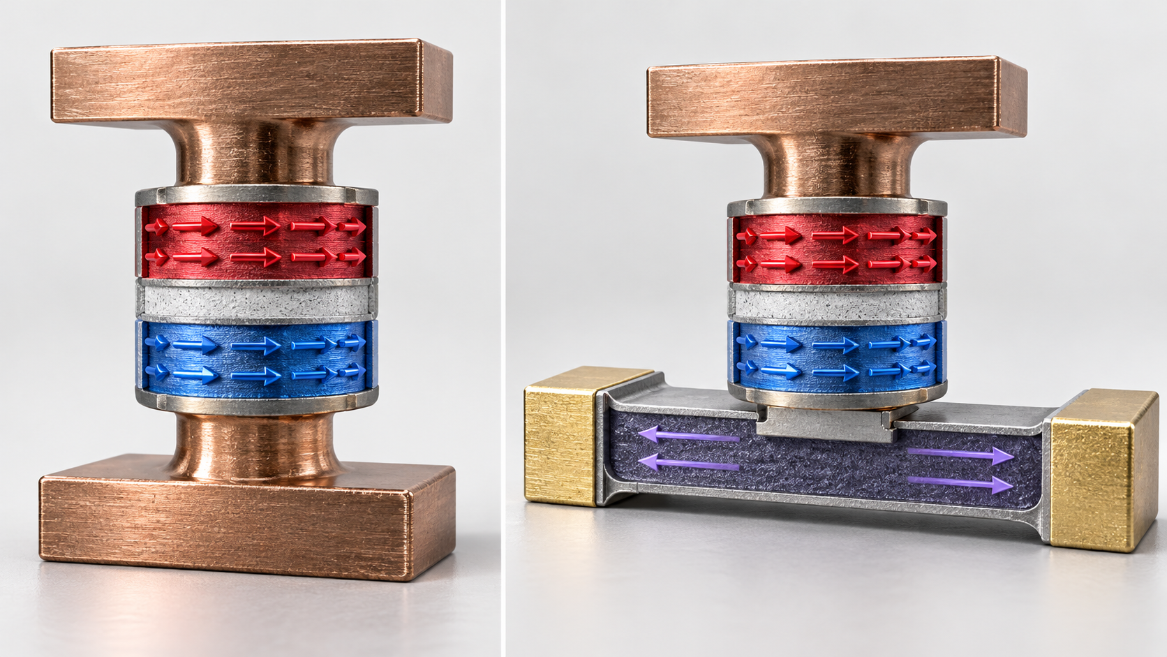
View the original SVG schematic and exact annotations
The SOT type sends the write current not through the MTJ but through a heavy-metal strip under the free layer. Miron et al. showed at room temperature, in Pt/Co/AlOx, reversal of perpendicularly magnetized cobalt by in-plane current alone [Source 7]. Liu et al. used the spin Hall effect of β-Ta to reverse in-plane and perpendicular ferromagnetic layers by spin torque, and showed a three-terminal device with an MTJ for readout [Source 8]. According to Dieny et al., SOT-MRAM has cache-compatible speed and high endurance, at the cost of larger write currents and a larger footprint. The method that changes anisotropy by voltage (VCMA) gives too small a change at ordinary voltage (about 1 V), and reconciling switching with thermal stability in standby remains a problem [Source 1]. For the products and mass production of MRAM, see the “Nanomemory” article of this series.
The perpendicular MTJ of Ikeda et al. has a write current of 49 µA at 40 nm diameter [Source 6]. Our calculation The cross-section is π × (20 nm)² = about 1.26 × 10⁻¹¹ cm², so the current density is 49 µA ÷ 1.26 × 10⁻¹¹ cm² = about 3.9 MA/cm². Applying the target for STT current given by Dieny et al., “below 2 MA/cm²” [Source 1], to the same 40 nm diameter gives about 25 µA (2 MA/cm² × 1.26 × 10⁻¹¹ cm²).
Assumptions and limits: the MTJ cross-section is assumed to be a circle of 40 nm diameter. A write current changes with pulse width and with how probability is defined, and the abstract of the paper does not give these. The target shows a direction of research, not a product specification.
The force that keeps the free layer’s magnetization in place is expressed by the thermal stability factor Δ (the energy barrier divided by kBT). Our calculation Assuming retention time τ = τ0·exp(Δ) and an attempt time τ0 = 1 ns, the Δ needed for 10 years (about 3.16 × 10⁸ s) is ln(3.16 × 10⁸ s ÷ 1 ns) = about 40. At 300 K, kBT is about 4.14 × 10⁻²¹ J, so 40 kBT = about 0.17 aJ. This is of the same order as the “0.1 aJ” that Dieny et al. give for the energy barrier to switch a nanomagnet [Source 1].
Δ is proportional to volume. If the diameter is halved with the same thickness and the same effective anisotropy, the volume becomes a quarter and so does Δ (Fig. 5). If Δ is 40 at 40 nm, say, it is about 10 at 20 nm, and retention drops to 1 ns × e10 = about 22 µs. The remedy is a roughly fourfold effective anisotropy, or a thicker free layer. The latter is the idea of STT-MRAM using perpendicular shape anisotropy that Dieny et al. describe (a thicker storage layer, so that shape anisotropy adds to the interfacial one), which is said to give a large Δ even below 10 nm [Source 1].
Assumptions and limits: τ0 = 1 ns is a rule-of-thumb assumption. Real retention specifications depend on the number of cells and the tolerated failure rate and may need a larger Δ than this calculation. The calculation is not data for a real device.
The perpendicular anisotropy of CoFeB/MgO is born at the transition-metal/oxide interface [Sources 1, 6, 21]. Per unit volume of the layer, an interfacial anisotropy counts for more the thinner the layer is (a geometric view). The free layer can therefore only be made thin, and as scaling reduces its volume, Δ falls (calculation 3).
Dieny et al. say that current MTJ stacks are complex and relatively thick (about 20 nm), which hinders ion-beam etching and sets a lower limit on the cell pitch [Source 1]. Anisotropy is earned at the interface, while processing is limited by the thickness of the stack. This squeeze is the background to the ideas of a thicker storage layer and of stacks with two tunnel barriers (described by Dieny et al.) (commentary by this article).
5. Materials that generate spin current — heavy metals and their resistivity
The efficiency of the SOT type is decided by the spin Hall angle, the proportion θSH = JS / Je of transverse spin current JS produced from a charge current Je. Liu et al. reported that tantalum in its high-resistivity (β) form has a spin Hall angle of 0.12–0.15 by three independent methods, larger than the about 0.07 of Pt and of the opposite sign. The resistivity of Ta is about 190 µΩ·cm, and they confirmed the β phase. As a difference from Pt, they also note that Ta does not significantly raise the magnetic damping of the neighbouring thin-film magnet [Source 8].
- A tug of war between resistivity and efficiency: the high resistivity of β-Ta (about 190 µΩ·cm) means less current flows for the same voltage. Dieny et al. say that reducing the write current requires development of charge-spin conversion materials with low resistivity and high SOT efficiency [Source 1]
- New candidates: the same review introduces ferromagnet/topological-insulator bilayers, which may raise the efficiency of SOT switching, and transition-metal dichalcogenide (TMDC)/ferromagnet bilayers, in which crystal symmetry can be used to engineer SOT [Source 1]. Both are at the stage of “potential”, and the lack of large-area deposition tools is taken up in Chapter 8
θSH is an index of how efficiently spin current is made, but the size of the current that can be sent through the device is set by the resistivity and thickness of the heavy-metal layer. β-Ta showed a large θSH together with a high resistivity [Source 8]. Liu et al. also point out that for Ta the way the efficiency is measured can produce a large error in the estimate. A low value reported with a non-local spin valve was an underestimate, they explain, because the analysis did not correctly treat how current is shunted by a highly conducting Cu electrode [Source 8].
From the materials side, θSH, resistivity, thickness, interface transparency and crystal phase (β or α) have to be optimized together, and a comparison of θSH values alone is only the entrance to choosing a material (commentary by this article).
6. Heusler alloys — the hope of half-metals, and the wall of temperature
Heusler alloys are alloys theoretically predicted to be “half-metals”, ferromagnets in which only one spin direction is metallic and the other is insulating, so that spin polarization reaches 100%. The review by Elphick et al. lists as advantages of Heusler alloys good lattice matching with major substrates, a Curie temperature above room temperature, and the ability to control the spin density of states near the Fermi level as intermetallic compounds. It organizes the point that proving half-metallicity at room temperature requires structural and magnetic characterization on an atomic scaleSourced [Source 19].
- Spin polarization: in epitaxial Co2MnSi thin films, an exceptionally large spin polarization of 93% at room temperature was directly observed by ultraviolet photoemission spectroscopy (a surface-sensitive method, with bulk-sensitive measurements also consistent with calculation) [Source 18]. Dieny et al. state that Heusler alloys have shown 100% spin polarization at room temperature, and describe how the crystallization temperature has recently dropped from above 400 °C to below 135 °C, making them easier to put into devices without interfacial mixing [Source 1]. Values differ between papers, so the measurement method and the sample need to be read with them
- TMR ratio: Liu et al. reported, for epitaxial Co2MnSi/MgO/Co2MnSi MTJs, up to 1995% at 4.2 K and up to 354% at 290 K [Source 9]
Our calculation In the Co2MnSi MTJs of Liu et al., 354 ÷ 1995 = about 18% remains at room temperature (290 K) [Source 9]. For comparison, in the CoFeB/MgO/CoFeB of Ikeda et al., 604 ÷ 1144 = about 53% (room temperature 300 K and 5 K) [Source 5].
Assumptions and limits: the two are different stacks, annealing and temperatures (290 K and 300 K, 4.2 K and 5 K), so this is not a comparison under the same conditions. It is also not the temperature dependence of a single device, and it does not conclude that Heusler alloys are inferior. How far the half-metallicity of Heusler alloys is lost with temperature or interface disorder has not been checked in the sources used here.
Elphick et al. explain that the atomic ordering of Heusler films can be examined directly by X-ray diffraction and indirectly through the temperature dependence of electrical resistivity, and that element-specific magnetic moments and spin polarization are measured by X-ray magnetic circular dichroism and Andreev reflection [Source 19]. That is, not only composition but which atom sits on which site governs half-metallicity.
This links directly to process conditions. Ordering needs heat, and heat invites interfacial mixing. The effort to lower the crystallization temperature to below 135 °C [Source 1] can be read as aiming at ordering and interface protection together (commentary by this article). The design thinking differs from MgO systems, which sit on stacks that allow annealing at the 500 °C level.
7. New material classes — skyrmions, antiferromagnets, two-dimensional magnets
From here the material classes are still at the research stage. Fig. 6 brings together the range organized by Dieny et al. for phenomena at technology readiness level (TRL) 3 or above, and related primary sources.
(1) Skyrmions
A skyrmion is a small topologically protected structure in which the magnetization winds like a vortex. Mühlbauer et al. observed by neutron scattering the spontaneous formation of a two-dimensional lattice of skyrmion lines in the chiral magnet MnSi. The lattice is stable at the border between paramagnetism and long-range helical magnetic order (below a critical temperature Tc = 29.5 K)Sourced [Source 10]. According to the review by Fert et al., skyrmions can be nanometres in diameter and behave as particles that can be moved, created and annihilated. Until recently they were observed only at low temperature and under large fields, but thin-film and multilayer structures have been found in which they are stable at room temperature and can be manipulated by electrical currents. Writing, processing and reading at room temperature by all-electrical means remain challengesSourced [Source 20]. Woo et al. reported stable skyrmions at room temperature in ultrathin transition-metal ferromagnetic films, and the motion of skyrmions along a racetrack by current pulses [Source 11]. Dieny et al. give domain walls and skyrmions as examples of the information carried along a narrow track in “racetrack memory” [Source 1].
(2) Antiferromagnets
In an antiferromagnet the magnetic moments of neighbouring atoms alternate and the net magnetization is zero. Jungwirth et al. give as advantages that, as a result, information is invisible to external magnetic fields, insensitive to disturbing fields, and does not magnetically affect neighbouring elements however densely they are packed, and that dynamic responses are fast; the hard part is how to manipulate and detect the state efficiently [Source 13].
- Writing: Wadley et al. showed, in thin-film devices of the antiferromagnet CuMnAs, electrical switching between stable states at room temperature by currents of order 106 A/cm². Readout is also electrical, and the stored state is insensitive to external fields [Source 14]
- Reading: Nakatsuji et al. reported, in Mn3Sn, an antiferromagnet with non-collinear 120-degree spin order, a large anomalous Hall conductivity of about 20 Ω−1cm−1 at room temperature and over 100 Ω−1cm−1 at low temperature. The magnetization is extremely small, about 0.002 µB per Mn atom, and the sign can be reversed by a field of a few hundred oersted [Source 15]
- Frequency: Dieny et al. state that the strong exchange coupling of antiferromagnets pushes the corresponding frequencies into the THz range [Source 1]
(3) Two-dimensional magnets
Can magnetic order hold in a two-dimensional material? Huang et al. showed with magneto-optical Kerr effect microscopy that monolayer CrI3 is an Ising ferromagnet with out-of-plane spin orientation. Its Curie temperature is 45 K, slightly lower than the 61 K of the bulk crystal; they report a layer dependence in which magnetization is suppressed in two layers (a metamagnetic effect) and ferromagnetism is restored in three layersSourced [Source 16]. Gong et al. observed intrinsic long-range ferromagnetic order in atomic layers of Cr2Ge2Te6, and reported that a small field of 0.3 T or less raises the transition temperature by 35–57% [Source 17].
For MTJ applications, Song et al. reported spin-filter devices with CrI3 as the barrier and graphene as electrodes, in which the TMR ratio increases with the number of layers and reaches 19,000% for four layers (at low temperature), explained by the layer-by-layer antiferromagnetic order [Source 12]. Dieny et al. present this value as a record at low temperature and also introduce a report of a TMR ratio above 50% in Co/hBN/Fe with a hexagonal boron nitride (hBN) barrier [Source 1].
The giant TMR ratio of two-dimensional magnets (19,000%) and part of the observations of skyrmions are reports at low temperature and under large fields. A record as a room-temperature, zero-field device could not be confirmed within the scope of this article. As Fig. 3 shows, “19,000%” is a value obtained only at low temperatureNot yet confirmed.
8. Walls of materials and process — will it fit on a 300 mm wafer?
The materials-side challenges that Dieny et al. list are as follows [Source 1].
- Stack thickness and processing: MTJ stacks are complex and relatively thick (about 20 nm), hindering ion-beam etching and setting a lower limit on the spacing of cells. A 10 Gbit MRAM is given as a specific target
- Production tools for new materials: Co and Cu are also used in conventional electronics and are easy to integrate. Heusler alloys, topological insulators and two-dimensional materials, however, need development of large-scale production tools to transfer or directly grow them on 300 mm wafers. To put two-dimensional materials into MRAM, a way is also needed to deposit magnetic multilayers by PVD (sputtering), which industry favours, without damaging the properties of the two-dimensional material
- Testing and evaluation: for volume production and quality control, techniques are needed to evaluate the quality of tunnel barriers and the reliability of devices
- Logic and processing: spintronic logic will in practice be hybrid with CMOS; the conversion efficiency between spin and charge signals is low, and the energy spent in the CMOS periphery tends to outweigh the intrinsic saving in the magnetic part, they state
- Sensors: in cars, as electrified vehicles raise the accuracy demanded of magnetic sensors, the performance of spintronic sensors is not yet sufficient to replace shunt-based sensors for current measurement
Dieny et al. say that for new materials to move to higher TRL, high-quality nanostructured materials must be obtained over large areas [Source 1]. CoFeB/MgO is a system whose materials and tools have grown up so that it can be mass-produced by sputtering on 300 mm wafers. Even if Heusler alloys or two-dimensional magnets show excellent values in small laboratory samples, the next gate is whether they can be deposited uniformly over a large area, with a low thermal budget and without disturbing interfaces.
From the materials side, this field can be read as rewarding novelty that fits an existing mass-production line more than novelty of the crystal itself (commentary by this article).
9. Limits, and what could not be confirmed
(1) How far the sources were checked
For Baibich et al., Yuasa et al., Parkin et al., Ikeda et al., Miron et al., Liu et al. (Co2MnSi), Jourdan et al., Elphick et al., Nakatsuji et al., Wadley et al., Fert et al., Jungwirth et al., Huang et al., Gong et al., Song et al., Woo et al., and Dieny and Chshiev, only the abstract on the publisher’s page or in a preprint was checked, and the full text was not. The full text, or the full text of an accepted version or preprint, was read for Dieny et al. (review), Liu et al. (β-Ta) and Mühlbauer et al. (MnSi). The review by Dieny et al. is an accepted version of 2020, and progress since 2020 (including the state of mass production by companies) has not been checked in this article.
(2) What could not be confirmed
The JEDEC standards that define retention and writing of MRAM could not be confirmed, because the JEDEC site blocked automated access. No ISO, IEC or JIS standard that directly defines the magnetoresistance characteristics of an MTJ could be confirmed. How far the half-metallicity of Heusler alloys is lost with temperature and interfaces, and the practicality at room temperature of skyrmions and spintronic logic, have not been confirmed in the sources used here.
(3) Out of scope
Spin caloritronics, details of magnonics, spins for quantum computing, spin FETs, dilute magnetic semiconductors, probabilistic and neuromorphic computing, prices and market sizes are not covered. For MRAM products, mass production and company plans see the “Nanomemory” article; for permanent magnets, the “Permanent Magnets and Rare Earths” article.
- Performance is decided by the thin-film stack and its interfaces. The (001) orientation of MgO, the annealing of CoFeB and the suppression of Ta diffusion supported a room-temperature TMR ratio of 604%Sourced
- Perpendicular anisotropy is a property of the interface and hard to reconcile with scaling. Halving the diameter cuts Δ to about a quarterSourced / Our calculation
- For SOT materials the issue is a balance of spin Hall angle and resistivity. β-Ta has θSH of 0.12–0.15 and a resistivity of about 190 µΩ·cmSourced
- In Heusler alloys, atomic arrangement decides performance. 1995% at 4.2 K and 354% at 290 K have been reportedSourced
- Skyrmions, antiferromagnets and two-dimensional magnets are at the research stage. Many values are for low temperature and large fields, and room-temperature, all-electrical demonstrations remain a challengeNot yet confirmed
10. How to read evaluations and standards
The “performance” of spintronic materials is measured differently at each level: thin-film material properties (saturation magnetization, anisotropy, damping, spin Hall angle), device characteristics (TMR ratio, RA product, write current, thermal stability Δ), and memory-chip specifications (retention, endurance, magnetic-field immunity). Most of these are measured by methods specific to each paper, and this is not a field in which international standards are in place. In this article’s research, only an IEEE standards project on the magnetic-field immunity of MRAM (still being drafted) and an industry standard for reliability testing of automotive ICs could be confirmed.
| Item evaluated | ISO | IEC / IEEE | JIS | ASTM (number and title only) | What changes the value with measurement conditions |
|---|---|---|---|---|---|
| Magnetoresistance characteristics of MTJ and GMR devices (TMR ratio, RA product) | Could not be confirmed | Could not be confirmed | Could not be confirmed | Could not be confirmed | The definition of the TMR ratio (normalized to RP or to RAP), temperature, annealing temperature, bias voltage, the RA product (which changes with barrier thickness). They differ from paper to paper, so checking conditions is essential to compare values |
| Magnetic-field immunity of MRAM | Could not be confirmed | IEEE P3465 “IEEE Draft Standard for Magnetic Field Immunity Verification of Magnetoresistive Random Access Memory” (being drafted; the standards project was approved on 6 June 2024; sponsored by the IEEE Magnetics Society) [23] | Could not be confirmed | Could not be confirmed | According to the IEEE page, it plans to define measurement conditions for the maximum static field that still meets a prescribed bit error rate (read, write, power-off, standby) and a method of evaluating how the error rate degrades as the field increases. It is not yet established, and the content may change. JEDEC standards could not be confirmed because the JEDEC site blocked automated access |
| Reliability tests for automotive ICs including non-volatile memory | Could not be confirmed | Could not be confirmed | Could not be confirmed | Could not be confirmed | An industry-body standard: AEC-Q100 Rev-J1 “Failure Mechanism Based Stress Test Qualification For Integrated Circuits” and AEC-Q100-005 Rev-D1 “Non-Volatile Memory Program/Erase Endurance, Data Retention, and Operational Life Test” [24]. These are documents of the Automotive Electronics Council (AEC) and not international standards like those of ISO or IEC. Their application to MRAM has not been confirmed in this article |
| Magnetic properties of thin films (Ms, anisotropy, damping) and spin Hall angle | Could not be confirmed | Could not be confirmed | Could not be confirmed | Could not be confirmed | Magnetic properties change with sample form (thin film), temperature and method (magnetometry, ferromagnetic resonance and so on). The spin Hall angle can differ greatly with the method (Liu et al. obtained 0.12–0.15 by three independent methods, and point out that a non-local spin valve can underestimate through the treatment of current shunting) [8] |
The number, title and status of each standard in the rows are Sourced (checked on the IEEE standards-project page and the AEC document list; because IEEE P3465 is being drafted it is Not yet confirmed). The arrangement of the table is editorial work, which counts as Our calculation. The ASTM International site was not opened, and no applicable ASTM standard could be confirmed. The texts of standards were not checked.
Cautions when reading standards
- Where there is no standard, comparing the values in papers starts with checking conditions. For the TMR ratio check the definition, temperature, annealing, bias and RA product; for the spin Hall angle, the measurement method
- Do not write a standard that is still being drafted as if it were settled. IEEE P3465 is at the stage of an approved standards project (PAR), and what it specifies may change
- Documents of an industry body are not international standards. AEC-Q100 is a framework for reliability tests of automotive ICs and does not define the performance of a material. A memory-retention specification also depends on the number of cells and the tolerated failure rate, as in calculation (3) of this article
11. Glossary
- Spin
- The property of an electron as a tiny magnet; up or down, for example.
- GMR (giant magnetoresistance)
- A large change of resistance with the relative magnetization of two ferromagnetic layers around a non-magnetic metal.
- TMR (tunnel magnetoresistance)
- The same change of resistance in ferromagnetic layers across an insulator (a tunnel barrier).
- MTJ (magnetic tunnel junction)
- A device with two ferromagnetic layers across a tunnel barrier; the storage element of MRAM.
- RA product
- The product of the device’s resistance and area. It changes with barrier thickness.
- PMA (perpendicular magnetic anisotropy)
- The tendency of magnetization to point perpendicular to the film plane. Born at the CoFeB/MgO interface.
- STT (spin-transfer torque)
- Reversal of magnetization by the spin angular momentum of a current.
- SOT (spin-orbit torque)
- Reversal of magnetization by spin current from the spin Hall effect and similar effects.
- Spin Hall angle θSH
- The proportion of transverse spin current produced per unit charge current.
- Thermal stability factor Δ
- The energy barrier divided by kBT. An index of retention time.
- Heusler alloy
- An ordered alloy such as Co2MnSi. Half-metallicity is expected in theory.
- Half-metal
- A ferromagnet in which only one spin direction is metallic. Spin polarization reaches 100%.
- Skyrmion
- A small, topologically protected structure in which the magnetization winds like a vortex.
- Antiferromagnet
- A material in which neighbouring magnetic moments alternate and the net magnetization is zero.
- Two-dimensional magnet
- A layered material that keeps magnetic order down to atomic layers (such as CrI3).
- TRL (technology readiness level)
- A scale of the stages from research to practical use.
12. References (primary sources)
- Dieny B. et al. “Opportunities and challenges for spintronics in the microelectronics industry”, Nat. Electron. 3, 446–459 (2020), DOI 10.1038/s41928-020-0461-5 (full text of the accepted version checked) — doi.org/10.1038/s41928-020-0461-5
- Baibich M. N. et al. “Giant Magnetoresistance of (001)Fe/(001)Cr Magnetic Superlattices”, Phys. Rev. Lett. 61, 2472–2475 (1988), DOI 10.1103/PhysRevLett.61.2472 (abstract only checked) — doi.org/10.1103/PhysRevLett.61.2472
- Yuasa S. et al. “Giant room-temperature magnetoresistance in single-crystal Fe/MgO/Fe magnetic tunnel junctions”, Nat. Mater. 3, 868–871 (2004), DOI 10.1038/nmat1257 (abstract only checked) — doi.org/10.1038/nmat1257
- Parkin S. S. P. et al. “Giant tunnelling magnetoresistance at room temperature with MgO (100) tunnel barriers”, Nat. Mater. 3, 862–867 (2004), DOI 10.1038/nmat1256 (abstract only checked) — doi.org/10.1038/nmat1256
- Ikeda S. et al. “Tunnel magnetoresistance of 604% at 300 K by suppression of Ta diffusion in CoFeB/MgO/CoFeB pseudo-spin-valves annealed at high temperature”, Appl. Phys. Lett. 93, 082508 (2008), DOI 10.1063/1.2976435 (abstract only checked) — doi.org/10.1063/1.2976435
- Ikeda S. et al. “A perpendicular-anisotropy CoFeB–MgO magnetic tunnel junction”, Nat. Mater. 9, 721–724 (2010), DOI 10.1038/nmat2804 (abstract only checked) — doi.org/10.1038/nmat2804
- Miron I. M. et al. “Perpendicular switching of a single ferromagnetic layer induced by in-plane current injection”, Nature 476, 189–193 (2011), DOI 10.1038/nature10309 (abstract only checked) — doi.org/10.1038/nature10309
- Liu L. et al. “Spin-Torque Switching with the Giant Spin Hall Effect of Tantalum”, Science 336, 555–558 (2012), DOI 10.1126/science.1218197 (full text of preprint arXiv:1203.2875 checked) — doi.org/10.1126/science.1218197
- Liu H. et al. “Giant tunneling magnetoresistance in epitaxial Co2MnSi/MgO/Co2MnSi magnetic tunnel junctions by half-metallicity of Co2MnSi and coherent tunneling”, Appl. Phys. Lett. 101, 132418 (2012), DOI 10.1063/1.4755773 (abstract only checked) — doi.org/10.1063/1.4755773
- Mühlbauer S. et al. “Skyrmion Lattice in a Chiral Magnet”, Science 323, 915–919 (2009), DOI 10.1126/science.1166767 (full text of preprint arXiv:0902.1968 checked) — doi.org/10.1126/science.1166767
- Woo S. et al. “Observation of room-temperature magnetic skyrmions and their current-driven dynamics in ultrathin metallic ferromagnets”, Nat. Mater. 15, 501–506 (2016), DOI 10.1038/nmat4593 (abstract of preprint arXiv:1502.07376 checked) — doi.org/10.1038/nmat4593
- Song T. et al. “Giant tunneling magnetoresistance in spin-filter van der Waals heterostructures”, Science 360, 1214–1218 (2018), DOI 10.1126/science.aar4851 (abstract of preprint arXiv:1801.08679 checked) — doi.org/10.1126/science.aar4851
- Jungwirth T. et al. “Antiferromagnetic spintronics”, Nat. Nanotechnol. 11, 231–241 (2016), DOI 10.1038/nnano.2016.18 (abstract only checked) — doi.org/10.1038/nnano.2016.18
- Wadley P. et al. “Electrical switching of an antiferromagnet”, Science 351, 587–590 (2016), DOI 10.1126/science.aab1031 (abstract only checked) — doi.org/10.1126/science.aab1031
- Nakatsuji S., Kiyohara N., Higo T. “Large anomalous Hall effect in a non-collinear antiferromagnet at room temperature”, Nature 527, 212–215 (2015), DOI 10.1038/nature15723 (abstract only checked) — doi.org/10.1038/nature15723
- Huang B. et al. “Layer-dependent ferromagnetism in a van der Waals crystal down to the monolayer limit”, Nature 546, 270–273 (2017), DOI 10.1038/nature22391 (abstract of preprint arXiv:1703.05892 checked) — doi.org/10.1038/nature22391
- Gong C. et al. “Discovery of intrinsic ferromagnetism in two-dimensional van der Waals crystals”, Nature 546, 265–269 (2017), DOI 10.1038/nature22060 (abstract of preprint arXiv:1703.05753 checked) — doi.org/10.1038/nature22060
- Jourdan M. et al. “Direct observation of half-metallicity in the Heusler compound Co2MnSi”, Nat. Commun. 5, 3974 (2014), DOI 10.1038/ncomms4974 (open access; abstract only checked) — doi.org/10.1038/ncomms4974
- Elphick K. et al. “Heusler alloys for spintronic devices: review on recent development and future perspectives”, Sci. Technol. Adv. Mater. 22, 235–271 (2021), DOI 10.1080/14686996.2020.1812364 (open access; abstract only checked) — doi.org/10.1080/14686996.2020.1812364
- Fert A., Reyren N., Cros V. “Magnetic skyrmions: advances in physics and potential applications”, Nat. Rev. Mater. 2, 17031 (2017), DOI 10.1038/natrevmats.2017.31 (abstract only checked) — doi.org/10.1038/natrevmats.2017.31
- Dieny B., Chshiev M. “Perpendicular magnetic anisotropy at transition metal/oxide interfaces and applications”, Rev. Mod. Phys. 89, 025008 (2017), DOI 10.1103/RevModPhys.89.025008 (abstract only checked) — doi.org/10.1103/RevModPhys.89.025008
- Žutić I., Fabian J., Das Sarma S. “Spintronics: Fundamentals and applications”, Rev. Mod. Phys. 76, 323–410 (2004), DOI 10.1103/RevModPhys.76.323 (abstract of preprint arXiv:cond-mat/0405528 checked) — doi.org/10.1103/RevModPhys.76.323
- IEEE Standards Association “IEEE P3465 — IEEE Draft Standard for Magnetic Field Immunity Verification of Magnetoresistive Random Access Memory” (standards-project page; checked 10 October 2026) — standards.ieee.org/ieee/3465/11680
- Automotive Electronics Council (AEC) AEC document list (titles of AEC-Q100 Rev-J1 and AEC-Q100-005 Rev-D1; checked 10 October 2026) — aecouncil.com/AECDocuments.html
- Nobel Foundation “The Nobel Prize in Physics 2007” (laureates: Albert Fert, Peter Grünberg) — nobelprize.org/prizes/physics/2007/summary/
13. Claim-to-source audit
| Claim in the text | Basis | Category |
|---|---|---|
| Practical use of GMR spin valves and MTJs as read heads and position sensors; the embedded-cache use of STT-MRAM; the three functions of spintronic devices (read, write, carry); logic being at a conceptual stage (few demonstrations beyond TRL 3); the standard MTJ materials (transition metals, alloys, MgO); that 604% was reported about ten years earlier; the difficulty of reconciling large TMR and reliability as MgO thins; the insufficient TMR of perpendicular MTJs and read amplification; the consideration of alternatives to MgO or a return to GMR; typical TMR sensor values (about 200%, temperature coefficient, detectivity); the STT current target (below 2 MA/cm²); the pros and cons of SOT-MRAM; the problems of VCMA; the MTJ stack of about 20 nm and etching limits; perpendicular shape anisotropy; the 0.1 aJ barrier of a nanomagnet; the need for low-resistivity, high-SOT-efficiency materials; the potential of topological insulators and TMDCs; 100% spin polarization of Heusler alloys and the crystallization temperature (above 400 °C to below 135 °C); hBN barriers (TMR above 50%); the need for 300 mm production tools for new materials; hybrid logic with CMOS and periphery energy; sensors versus shunt-based sensors; the frequency of antiferromagnets (THz); racetrack memory | Review by Dieny et al. (2020, accepted version) Reference 1 https://doi.org/10.1038/s41928-020-0461-5 | Sourced |
| Giant magnetoresistance in Fe/Cr superlattices (Cr 9 Å, 4.2 K, 2 T), with resistivity falling by almost half | Abstract of Baibich et al. (1988) Reference 2 https://doi.org/10.1103/PhysRevLett.61.2472 | Sourced |
| Al-O barrier MTJs up to about 70% at room temperature; 180% at room temperature in single-crystal Fe/MgO/Fe; coherent spin-polarized tunnelling; oscillation of TMR with barrier thickness | Abstract of Yuasa et al. (2004) Reference 3 https://doi.org/10.1038/nmat1257 | Sourced |
| About 220% at room temperature and about 300% at low temperature with a (100)-oriented MgO barrier and CoFe electrodes; spin polarization of about 85%; thermal stability up to 400 °C | Abstract of Parkin et al. (2004) Reference 4 https://doi.org/10.1038/nmat1256 | Sourced |
| 604% at room temperature and 1144% at 5 K in CoFeB/MgO/CoFeB pseudo-spin-valve MTJs after annealing at 525 °C; the importance of annealing above 500 °C and of suppressing Ta diffusion; (001) orientation and stress relaxation of MgO | Abstract of Ikeda et al. (2008) Reference 5 https://doi.org/10.1063/1.2976435 | Sourced |
| Perpendicular Ta/CoFeB/MgO/CoFeB/Ta MTJ (TMR above 120%, high thermal stability down to 40 nm diameter, write current 49 µA); the same material combination as conventional MTJs | Abstract of Ikeda et al. (2010) Reference 6 https://doi.org/10.1038/nmat2804 | Sourced |
| Reversal of perpendicular magnetization by in-plane current in Pt/Co/AlOx (room temperature) | Abstract of Miron et al. (2011) Reference 7 https://doi.org/10.1038/nature10309 | Sourced |
| Spin Hall angle of β-Ta of 0.12–0.15 (Pt about 0.07); resistivity of Ta about 190 µΩ·cm; the three-terminal device; that Ta does not raise damping greatly; the explanation of underestimation with a non-local spin valve | Full text of the preprint of Liu et al. (2012) Reference 8 https://doi.org/10.1126/science.1218197 | Sourced |
| Up to 1995% at 4.2 K and up to 354% at 290 K in Co2MnSi/MgO/Co2MnSi MTJs | Abstract of Liu et al. (2012) Reference 9 https://doi.org/10.1063/1.4755773 | Sourced |
| A skyrmion lattice observed by neutron scattering in MnSi; critical temperature 29.5 K | Mühlbauer et al. (2009) Reference 10 https://doi.org/10.1126/science.1166767 | Sourced |
| Room-temperature skyrmions in ultrathin transition-metal ferromagnetic films and their motion by current pulses | Abstract of Woo et al. (2016) Reference 11 https://doi.org/10.1038/nmat4593 | Sourced |
| CrI3 spin-filter MTJs (19,000% for four layers, at low temperature) | Abstract of Song et al. (2018) Reference 12 https://doi.org/10.1126/science.aar4851 | Sourced |
| Advantages of antiferromagnets (insensitive to external fields, no effect on neighbours, high frequencies) and the challenge (manipulation and detection) | Abstract of Jungwirth et al. (2016) Reference 13 https://doi.org/10.1038/nnano.2016.18 | Sourced |
| Electrical switching of CuMnAs at room temperature (about 106 A/cm²) | Abstract of Wadley et al. (2016) Reference 14 https://doi.org/10.1126/science.aab1031 | Sourced |
| Anomalous Hall conductivity of Mn3Sn (about 20 at room temperature, over 100 at low temperature, Ω−1cm−1); magnetization of about 0.002 µB per Mn | Abstract of Nakatsuji et al. (2015) Reference 15 https://doi.org/10.1038/nature15723 | Sourced |
| Monolayer CrI3 is ferromagnetic (45 K; bulk 61 K), suppressed in two layers, restored in three | Abstract of Huang et al. (2017) Reference 16 https://doi.org/10.1038/nature22391 | Sourced |
| Intrinsic ferromagnetism of Cr2Ge2Te6; transition temperature raised by 35–57% by 0.3 T or less | Abstract of Gong et al. (2017) Reference 17 https://doi.org/10.1038/nature22060 | Sourced |
| 93% spin polarization at room temperature in Co2MnSi thin films | Abstract of Jourdan et al. (2014) Reference 18 https://doi.org/10.1038/ncomms4974 | Sourced |
| The advantages of Heusler alloys, the need for atomic-scale evaluation to prove half-metallicity, and the ways of evaluating ordering | Abstract of Elphick et al. (2021) Reference 19 https://doi.org/10.1080/14686996.2020.1812364 | Sourced |
| Properties of skyrmions (nanometre diameter; moved, created, annihilated); from low temperature and large fields to room-temperature films; the challenge of room-temperature, all-electrical operation | Abstract of Fert et al. (2017) Reference 20 https://doi.org/10.1038/natrevmats.2017.31 | Sourced |
| Perpendicular magnetic anisotropy arising at metal/oxide interfaces | Abstract of Dieny and Chshiev (2017) Reference 21 https://doi.org/10.1103/RevModPhys.89.025008 | Sourced |
| The definition and basic principles of spintronics | Abstract of Žutić et al. (2004) Reference 22 https://doi.org/10.1103/RevModPhys.76.323 | Sourced |
| IEEE P3465 (magnetic-field immunity of MRAM; standards project approved 6 June 2024; being drafted) | IEEE standards-project page Reference 23 https://standards.ieee.org/ieee/3465/11680 | Not yet confirmed |
| Titles of AEC-Q100 Rev-J1 and AEC-Q100-005 Rev-D1 | AEC document list Reference 24 http://www.aecouncil.com/AECDocuments.html | Sourced |
| The laureates of the 2007 Nobel Prize in Physics (Fert, Grünberg) | Nobel Foundation page Reference 25 https://www.nobelprize.org/prizes/physics/2007/summary/ | Sourced |
| Conversion of TMR ratios into resistance ratios (about 1.7 times for 70%, 3 times for 200%, 3.2 times for 220%, about 7 times for 604%, about 12 times for 1144%); the current density of the write current (3.9 MA/cm² for 49 µA at 40 nm; about 25 µA at 2 MA/cm²); the thermal stability Δ (about 40 for 10 years, about 0.17 aJ, about a quarter when the diameter is halved, retention of about 22 µs at 20 nm); the room-temperature to low-temperature ratio of TMR (about 18% for Co2MnSi, about 53% for CoFeB) | Our calculation. It assumes the TMR definition (RAP − RP) / RP, a circular cross-section, τ = τ0exp(Δ) with τ0 = 1 ns, 300 K and scaling with volume. These are not values of real devices | Our calculation |
| ISO, IEC and JIS standards that define the magnetoresistance characteristics of MTJs; the JEDEC standards for MRAM; standards for thin-film magnetic properties and the spin Hall angle; the temperature and interface dependence of the half-metallicity of Heusler alloys; the room-temperature practicality of skyrmions and spin logic; progress after 2020; prices and market sizes | Could not be confirmed in the primary sources accessible within this article’s research, or not covered by the policy of this article, so not stated | Commentary |
| The readings that “performance is decided by crafting the interfaces”, “TMR is a phenomenon of crystal orientation and interface”, “perpendicular anisotropy is a property of the interface and works only in thin layers”, “a spin Hall angle alone does not make a usable material”, “half-metallicity is decided by atomic arrangement” and “the value of a new material is decided by the size it can be deposited at” | This article’s arrangement and commentary based on published content. They are not views stated by the authors or institutions | Commentary |
| That Figs. 2 to 4 and 6 are explanatory drawings, that Fig. 5 is a drawing that includes our calculation, and that Figs. 1 and 7 are AI-generated images, none of them measured figures or real data | Note from this article | Commentary |
Last updated 10 October 2026. Sources are limited to primary material (peer-reviewed papers, preprints, the Nobel Foundation, an IEEE standards-project page and the AEC document list). The texts of standards were not checked. The ASTM International site was not opened, because that body states that AI use of the site is not permitted. The JEDEC site could not be checked because it blocked automated access. For many papers only the abstract was checked, and the review by Dieny et al. is the accepted version of 2020. Values of magnetoresistance ratios, spin Hall angles and so on juxtapose reports with different temperatures, samples and annealing, and do not show which is better or easier to manufacture. Structural readings and materials-design interpretations are marked as Commentary and kept separate from sourced fact. An international standard for the magnetoresistance characteristics of MTJs, the JEDEC standards for MRAM, the temperature and interface dependence of the half-metallicity of Heusler alloys, the room-temperature practicality of skyrmions and spin logic, and progress after 2020 could not be confirmed and are not stated here. All figures are explanatory concept graphics. Figs. 2 to 4 and 6 are vector drawings, Fig. 5 is a drawing that includes our calculation, and Figs. 1 and 7 are AI-generated images, and none of them shows a real tool, device or product.