SEMICONDUCTOR FABRICATION · INTRODUCTION 1-3
Semiconductors in the AI Era
Why GPUs and HBM need more than faster arithmetic
A practical guide to the chips behind AI, the memory that feeds them, and the cooling, power and connections that determine what they can actually do.
- The question is no longer just “How fast can it calculate?”
- Why AI has become a semiconductor industry issue
- CPUs and GPUs: different ways to organise the work
- The memory wall: fast arithmetic needs a supply line
- The roofline model: two ceilings on performance
- HBM: put a wide memory interface close to the processor
- Heat: usable performance must fit a thermal budget
- Electricity demand reaches beyond the data centre
- Power delivery: distribute high, convert close to the load
- Four constraints, connected solutions
- Japan's role: materials, manufacturing and packaging
- What remains research rather than a production promise
- Bring the layers of the system together
- Check your understanding
- A short glossary
- Sources and reading notes
- Evidence map and calculation assumptions
Begin with the main text. The shaded physics boxes add optional detail and worked estimates. Figures are conceptual and not to scale. Numbered links lead to the supporting sources.
Explain why matrix-heavy AI workloads suit GPUs and specialised accelerators; use the memory wall and the roofline model to understand the need for HBM; and connect chip performance to packaging, cooling, power delivery and the electricity grid. The optional calculation boxes develop the reasoning without requiring you to read every number on your first pass.
The question is no longer just “How fast can it calculate?”
Ask an AI system to draft a paragraph and it may appear that the main challenge is doing more arithmetic. Inside the machine, however, the arithmetic units can spend much of their time waiting for data. Put more of them on a chip and two further problems grow: removing the heat and delivering enough electrical power.
This is the central thread of the chapter. AI hardware needs computation, data movement, cooling and power delivery to work together. A faster processor helps only if the rest of the system can support it.
Three ideas provide a useful starting point. First, much neural-network computation can be organised as many multiply-and-add operations, making parallel hardware attractive. Second, computation has improved faster than the bandwidth that supplies it. Third, a modern accelerator is part of a much larger system: memory stacks, packages, network links, racks and the local electricity infrastructure all influence its usable performance.
We will follow that chain from the arithmetic inside a chip to the power station outside the data centre.
Why AI has become a semiconductor industry issue
AI demand reaches far beyond the GPU itself. It creates demand for advanced logic, DRAM, HBM, packaging, networking and power components.
For context, WSTS's Spring 2026 forecast projected worldwide semiconductor sales of about US$1.51 trillion in 2026, roughly 90% above the previous year, with memory accounting for most of the expected increase. WSTS identified AI infrastructure, HBM and accelerated computing as major drivers. This is a dated forecast, not a full-year result. [60]
The Semiconductor Industry Association's 2026 industry report describes an AI server rack containing more than 4,500 semiconductor packages, with semiconductors representing over 95% of the rack's value. NVIDIA reported revenue of US$215.9 billion for its fiscal year ended in January 2026, up 65%, including US$193.7 billion from its data-centre business, up 68%. These examples indicate the scale of the shift; they do not describe every AI system. [61][62]
The technical story explains why the demand spreads across so many kinds of component.
CPUs and GPUs: different ways to organise the work
A CPU must cope well with many kinds of task: running an operating system, responding to events, following branches and executing a complicated sequence quickly. A GPU devotes much of its hardware to maintaining high throughput across many similar operations.
This is a difference in emphasis. CPUs also execute work in parallel, and GPUs also contain control logic and caches. A CPU core and a GPU arithmetic unit are not equivalent building blocks that can be compared simply by counting them. [1]
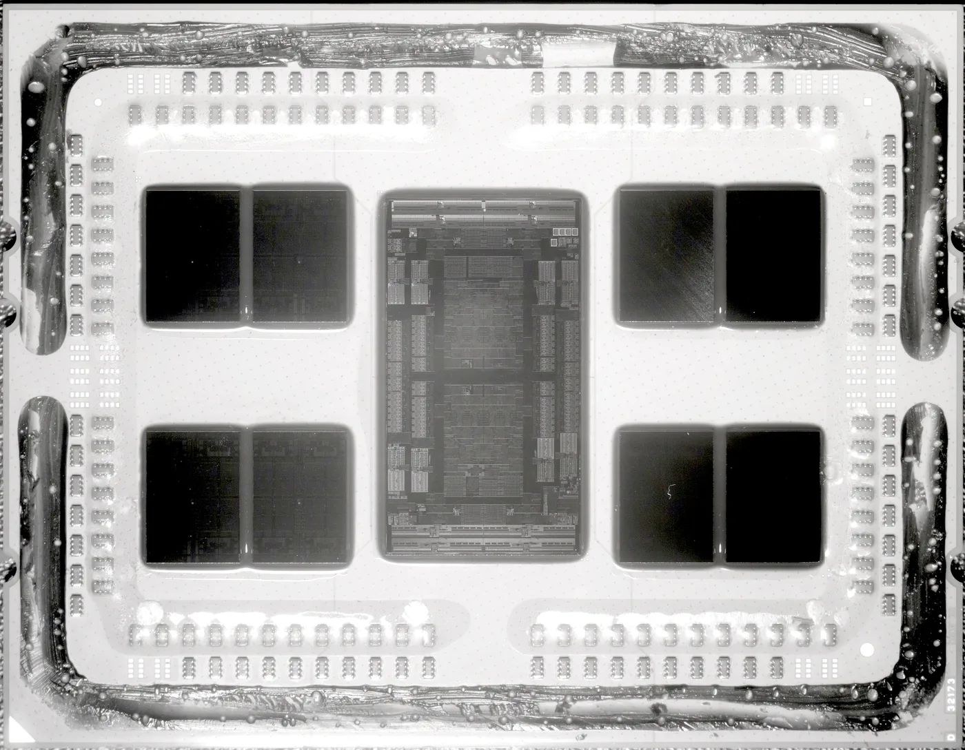
As an illustration of the counting problem, AMD's EPYC 9005 family includes processors with up to 192 CPU cores, while NVIDIA lists 21,760 CUDA cores for the GeForce RTX 5090. The numbers describe different structures and different ways of executing instructions. They are not a measure of one processor being a fixed multiple faster than the other. [2][3]
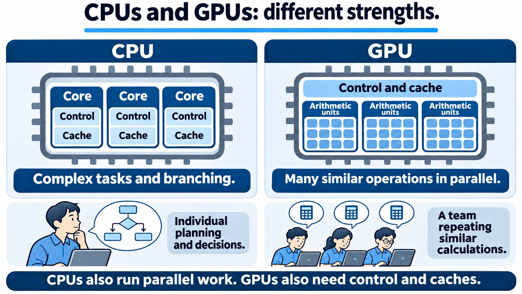
Reading the figure: Follow the allocation of resources, rather than the number of drawn boxes. Both processors need control and data storage; the balance differs.
Why matrix multiplication matters
A neural network repeatedly combines input values with learned weights. Much of that work can be expressed as matrix multiplication: multiply corresponding values, add the products, and repeat for many output elements.
One output element uses a row from the first matrix and a column from the second. Many output elements can be calculated independently once their inputs are available. This gives parallel hardware a large pool of useful work, although data dependencies between network layers and limits on memory bandwidth still exist.
Multiplying two square n × n matrices requires about n³ multiply-accumulate operations. A multiply-accumulate, or MAC, combines multiplication and addition; performance conventions commonly count those as two floating-point operations.
For n = 4096, n³ is about 68.7 billion MACs, or roughly 137 billion floating-point operations. Divide by an assumed peak of 50 PFLOPS and the ideal arithmetic-only time is about 2.7 microseconds. The 50 PFLOPS figure is the cited low-precision Rubin inference specification. Actual execution takes longer because of data movement, scheduling, numerical format and other constraints. This is a lower-bound calculation, not a benchmark. [10]
A dedicated approach: Google's TPU
An application-specific integrated circuit, or ASIC, can concentrate its resources on a narrower set of tasks. Google's first Tensor Processing Unit, described in its 2017 paper, contained 65,536 eight-bit MAC units in its matrix engine. On the workloads and systems studied, the authors reported approximately 15-30 times higher performance and 30-80 times higher performance per watt than the contemporary CPU and GPU comparisons. Those are historical study results, not universal ratios for today's hardware. [4]
The TPU used a systolic array: values move between neighbouring arithmetic cells in a coordinated rhythm. Reusing a value locally reduces the need to fetch it repeatedly from a more distant memory. The important insight is that the organisation of data movement can matter as much as the arithmetic unit itself.
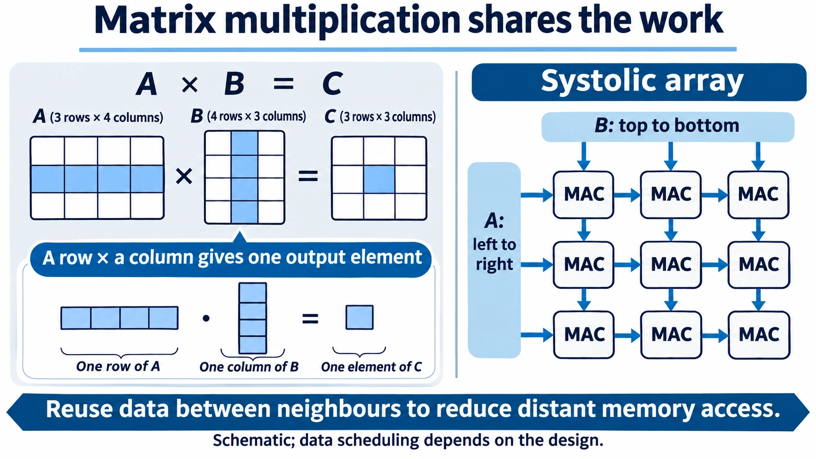
Reading the figure: A row and a column produce one output element. In the array, neighbouring cells reuse values as they move through the hardware. The drawing does not specify a complete timing schedule.
Reading accelerator specifications without turning them into a league table
The following figures are dated product-announcement and specification snapshots. Precision, sparsity, power definitions and benchmark conditions differ. Use the table to understand scale and design choices, rather than to rank products by one headline number.
| Product | Selected published figures | Sources |
|---|---|---|
| NVIDIA Blackwell | 208 billion transistors; two large dies connected at 10 TB/s; TSMC 4NP | [6] |
| NVIDIA Rubin | 336 billion transistors across two dies; 50 PFLOPS FP4 inference; 288 GB HBM4 at 19.2 TB/s | [9][10] |
| AMD Instinct MI355X | 185 billion transistors; 10.1 PFLOPS FP4; 288 GB HBM3E at 8 TB/s; 1400 W board power | [12] |
| AMD Instinct MI455X | Up to 40 PFLOPS FP4; 432 GB HBM4 at 23.3 TB/s | [13] |
| Google Ironwood TPU | 4614 TFLOPS per chip; 192 GB HBM at 7.37 TB/s; 42.5 exaFLOPS across 9216 chips | [5] |
| AWS Trainium3 | AWS's first 3 nm AI chip; 144 GB HBM3e at 4.9 TB/s | [14][15] |
| Microsoft Maia 200 | TSMC 3 nm; over 140 billion transistors; over 10 PFLOPS FP4; 216 GB HBM3e at 7 TB/s; 750 W | [16] |
FLOPS means floating-point operations per second. Tera is 1012, peta is 1015 and exa is 1018. Memory capacity, in GB, tells us how much can be held. Bandwidth, in TB/s, tells us how quickly data can be transferred. These answer different questions.
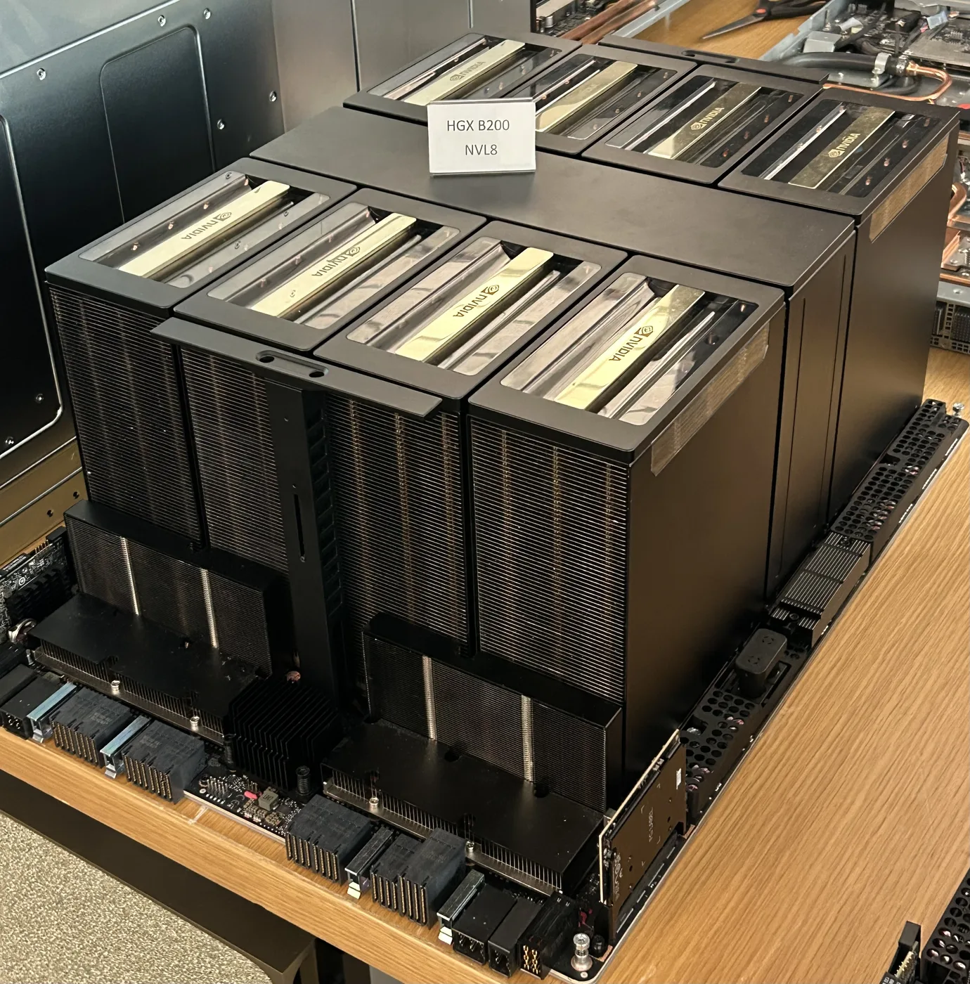
Three patterns stand out: transistor counts extend into hundreds of billions; low-precision arithmetic is prominent; and memory capacity and bandwidth sit alongside compute throughput as headline specifications. Some accelerators combine several logic dies within one package to obtain the desired scale.
Why lower precision can help
Numbers do not always need 32 or 64 bits. Some AI operations can use eight-bit or four-bit formats, provided suitable scaling, calibration and numerical methods preserve the required model quality. NVIDIA's Blackwell description includes micro-tensor scaling to support FP4 computation. This does not mean every operation in an AI application can be reduced to four bits without consequences. [6]
For a model with one trillion weights, sixteen-bit storage requires 2 TB for the raw weights; four-bit storage requires 0.5 TB. Those estimates exclude scaling metadata, activations, caches and other overheads. Reducing the raw weight size by four allows four times as many values through a fixed bandwidth, or four times as many in a fixed capacity.
Narrower arithmetic can also reduce circuit area and energy per operation. Lower precision therefore attacks both the arithmetic cost and the data-movement cost. Its value depends on retaining acceptable results.
Cloud accelerators and AI on a laptop
Large cloud providers can justify designing their own ASICs because they operate substantial, recurring workloads. AWS reported Trainium3 UltraServer improvements of up to 4.4 times the compute performance and four times the energy efficiency relative to its Trainium2 server comparison. Microsoft developed Maia 200 for inference, while Google reported Ironwood's performance per watt as twice that of its preceding TPU generation. These are vendor-specific comparisons with different baselines. [14][16][5]
The economic reasoning is straightforward: a sufficiently large workload can support the cost of a specialised design, while a narrower target may permit better performance per watt. That is an interpretation of the design strategy, not a guarantee that an ASIC always beats a GPU.
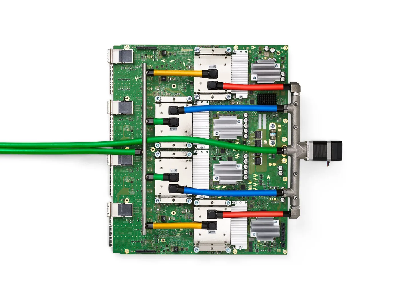
AI also runs locally. A neural processing unit, or NPU, is an AI-oriented engine within a PC or phone platform. Microsoft's original Copilot+ PC definition specified an NPU capable of at least 40 TOPS. Apple's M4 Neural Engine was announced at 38 trillion operations per second, and Qualcomm lists up to 85 TOPS for the Snapdragon X2 Elite NPU. TOPS comparisons still depend on the operation and numerical format being counted. [17–19]
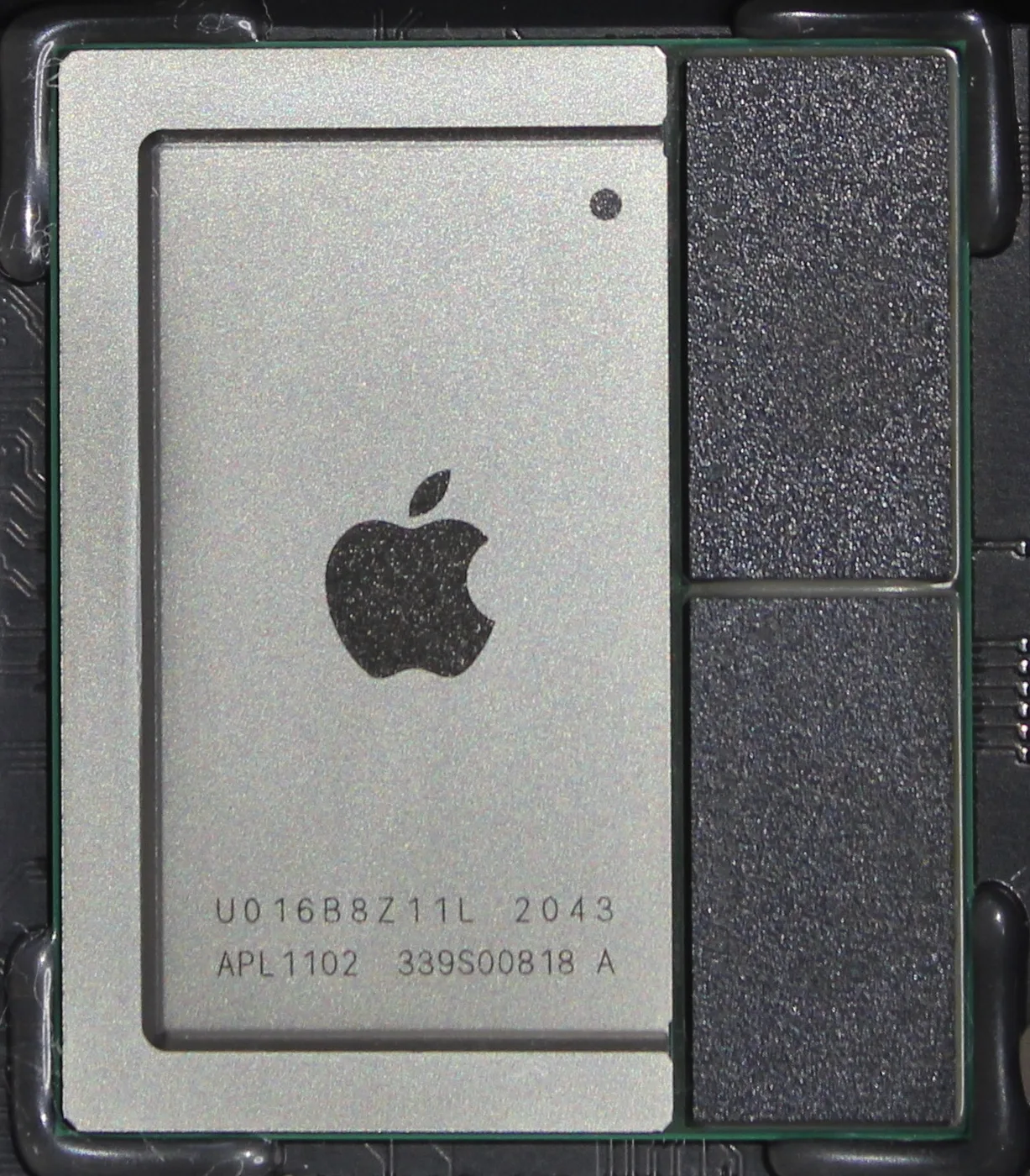
Local AI can reduce response time and the need to send data to a remote service. The cloud remains valuable for models and workloads beyond the capacity of the local device. The two approaches coexist.
The memory wall: fast arithmetic needs a supply line
Demand for training computation has grown rapidly. Epoch AI's analysis of frontier models over the period from 2010 to May 2024 found training compute increasing by roughly four to five times per year. That describes the selected models and period, not an indefinite law of nature. [20]
Hardware components have not improved at the same rate. In *AI and Memory Wall*, Gholami and colleagues summarised a roughly twenty-year period as follows. [21]
| Hardware measure | Representative growth per two years | Approximate growth over twenty years |
|---|---|---|
| Peak server compute throughput | 3.0× | 60,000× |
| DRAM bandwidth | 1.6× | 100× |
| Interconnect bandwidth | 1.4× | 30× |
The rounded growth rates and endpoints are a summary of historical trends. Their significance is the widening gap: adding arithmetic capacity is less useful when the data supply cannot keep pace.
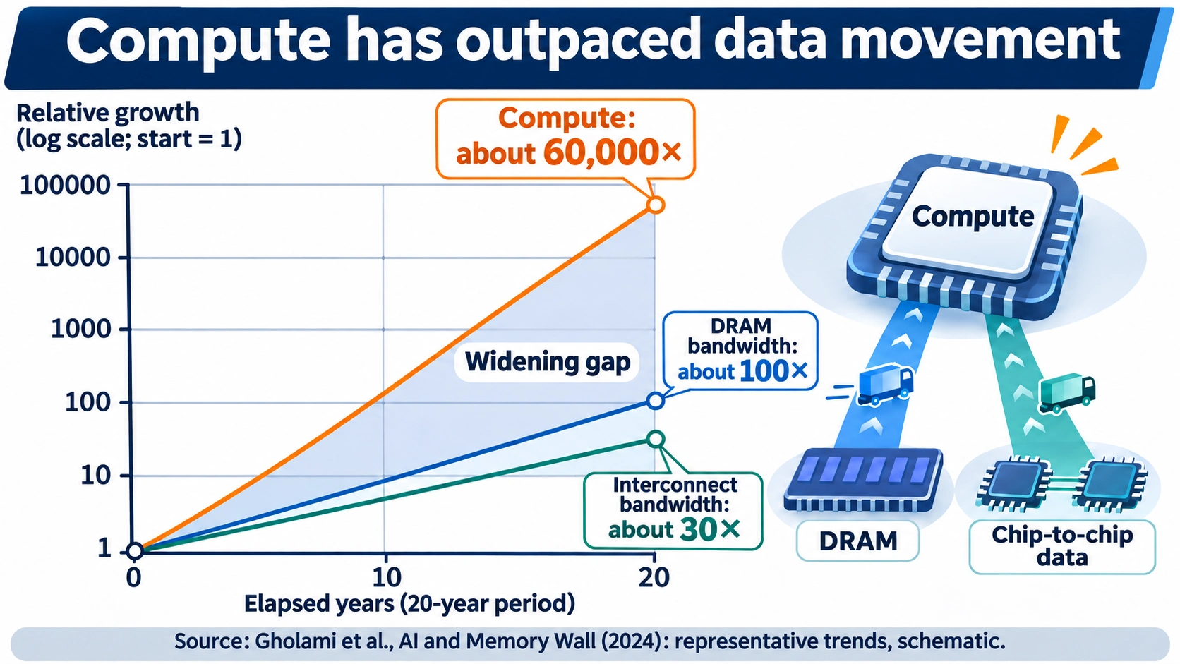
Reading the figure: Equal vertical distances represent equal ratios. The lines illustrate the paper's overall trends; they are not measurements for every intervening year or forecasts of future products.
Moving a bit also consumes energy
A wire has capacitance. Changing its electrical state requires charging and discharging that capacitance, with energy related to CV². Longer connections generally add capacitance and other costs, so retrieving data from a distant memory can consume much more energy than using a nearby value.
Mark Horowitz's 2014 ISSCC paper used illustrative figures of roughly 1-2 nJ for a DRAM access, versus around 10 pJ for certain on-chip accesses or operations, and discussed DRAM I/O energy around 10 pJ per bit. These are historical, operation-dependent examples, not specifications for every modern memory. Their enduring message is to count the cost of fetching data as well as the cost of calculating with it. [22]
As an intentionally unrealistic thought experiment, apply 10 pJ/bit to a continuous 19.2 TB/s data stream. Multiply by eight bits per byte and the result is approximately 1536 W. This is not an estimate of actual Rubin HBM power: it shows why using an old, high energy-per-bit assumption at modern bandwidth produces an untenable result. Short connections and efficient interfaces are essential.
The roofline model: two ceilings on performance
A workload does not have one fixed relationship to a processor's peak rating. The roofline model, developed by Williams, Waterman and Patterson, connects attainable throughput to arithmetic intensity: the number of operations performed per byte transferred from the memory level being considered. [23]
Performance upper bound = min(peak compute throughput, memory bandwidth × arithmetic intensity).
At low intensity, bandwidth is the limiting slope. At high intensity, the arithmetic units' peak throughput becomes the flat ceiling. Real performance can lie below either limit because of additional effects.
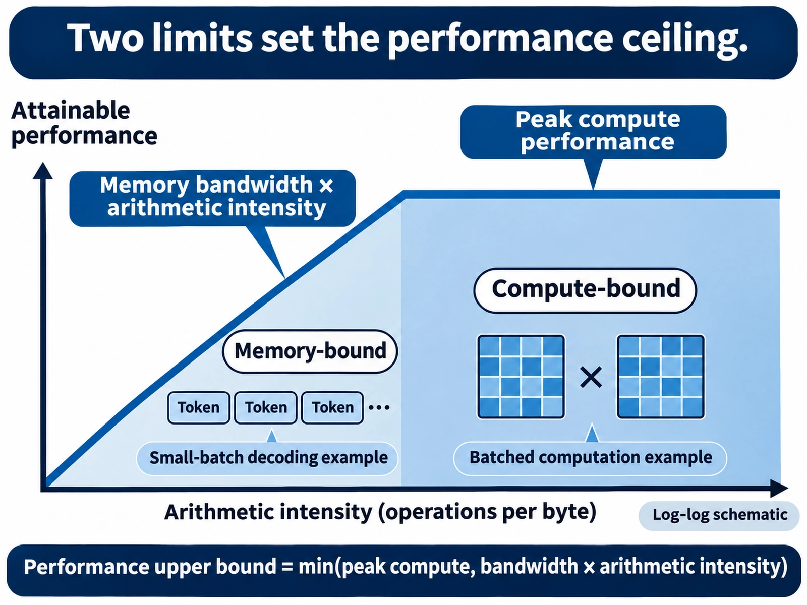
Reading the figure: Moving right means doing more work with each byte fetched. Reusing data can improve performance even if neither the chip's peak throughput nor its memory bandwidth changes.
Take the cited Rubin figures of 50 PFLOPS for FP4 inference and 19.2 TB/s of memory bandwidth. Their ratio is approximately 2600 operations per byte. This is an illustrative crossover using those headline ratings; numerical format and sparsity conventions must match when applying the model rigorously. [10]
Now imagine decoding one sequence at a time, reading each four-bit weight once for each new token. One weight occupies 0.5 bytes and contributes about two operations, giving 2/0.5 = 4 operations per byte in this simplified weight-only model. That is far below 2600.
The resulting bandwidth-limited estimate is about 0.15% of the stated peak compute rating. It is not a measurement of GPU utilisation, and it does not describe every inference workload. NVIDIA's inference discussion similarly distinguishes bandwidth-sensitive decoding from more compute-intensive phases and batching. [24]
If 288 GB were entirely occupied by weights, reading them once at 19.2 TB/s would take about 15 milliseconds, corresponding to about 67 tokens per second for that single-sequence thought experiment. It excludes attention-cache traffic, communication, overheads and capacity reserved for other purposes. Tokens are pieces of text, not necessarily whole words.
Batching several requests allows a weight read to serve more work, increasing arithmetic intensity. It also changes latency and scheduling trade-offs. This is why the workload and serving strategy must accompany any speed claim.
HBM: put a wide memory interface close to the processor
High-bandwidth memory, or HBM, stacks DRAM dies and connects them vertically using through-silicon vias, or TSVs. In a common 2.5D package, HBM stacks sit beside the logic dies on an interposer, allowing many short connections between them. CoWoS is TSMC's family of technologies for such integration; implementations vary. [28][29]
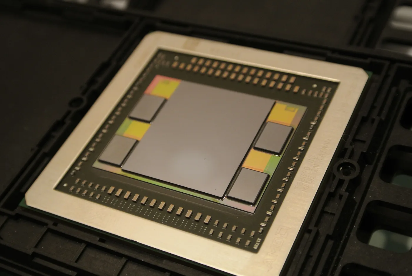
HBM raises the bandwidth part of the roofline in three related ways: a wide interface supplies many bits in parallel, short connections reduce transfer costs, and stacking provides capacity within the available package footprint.
The HBM4 standard announced by JEDEC in April 2025 specified a 2048-bit interface and up to 8 Gb/s per pin, giving roughly 2 TB/s per stack. It supported 4-, 8-, 12- and 16-high stacks and capacity up to 64 GB per stack. These are the cited standard's parameters, not a claim that every product uses its maximum configuration. [25]
Later vendor products advertised higher rates under their own specifications. SK hynix described speeds above 10 Gb/s and over 40% better power efficiency in its HBM4 development announcement. Samsung advertised up to 3.3 TB/s per stack, 12-high capacities of 24-36 GB and a 4 nm logic base die, with a stated 40% efficiency improvement against its comparison. Micron lists more than 2.8 TB/s per HBM4 stack. Each percentage needs its own baseline. [26–28]
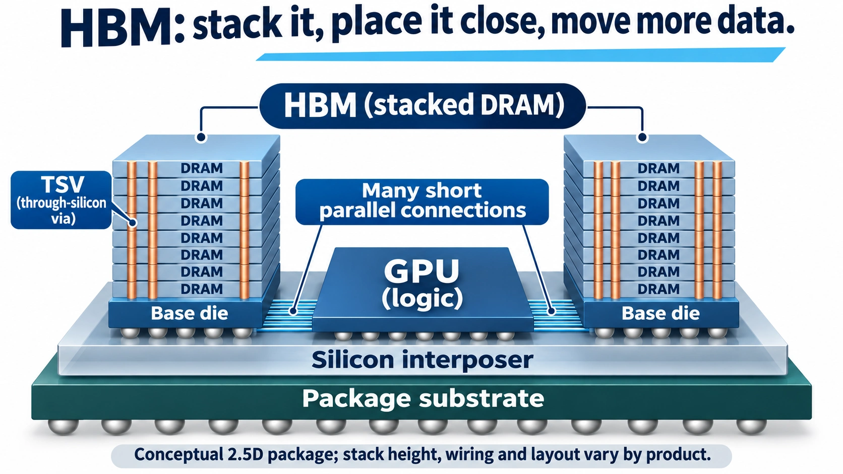
Reading the figure: DRAM is stacked within each HBM assembly. In this arrangement, those assemblies are beside the GPU, not directly on top of it. The base die, interposer and package substrate have separate jobs.
Why supply is difficult to expand
HBM combines demanding DRAM fabrication with thinning, stacking, dense connections and testing. Defects in a constituent die or an interconnect can compromise a stack, so known-good-die screening, process control and redundancy matter. Capacity cannot be increased simply by ordering more of an ordinary memory package.
In its October 2026 results discussion, SK hynix expected demand to exceed supply through 2030 and said long-term agreements covered more than half its 2027-2028 production capacity. Samsung's third-quarter 2026 results described strong server demand and constrained supply contributing to higher memory prices across applications. These are dated company assessments, not assured future outcomes. [30][31]
Allocating more resources to HBM can also affect the availability of other DRAM products. That is a supply-chain interpretation; the size of the effect depends on actual capacity allocation and demand.
Beyond a conventional memory stack
SK hynix describes using TSMC logic processes for HBM4 base dies, moving towards customer-specific HBM and exploring 3D stacked DRAM on logic. A logic-process base die can do more than support a stack physically: it can provide sophisticated interface and control functions. [68]
Another direction is processing-in-memory, or PIM. Samsung's 2021 HBM-PIM announcement placed AI arithmetic within memory banks and reported more than twice the system performance with over 70% lower energy use in its demonstration comparison. The goal is to avoid some data transfers, not to make all other processing disappear. [63]
Heat: usable performance must fit a thermal budget
The published power figures are substantial, but their definitions need care. NVIDIA lists up to 700 W TDP for an H100 configuration; AMD lists 1400 W total board power for MI355X; and a DGX B200 system with eight GPUs has a maximum system rating around 14.3 kW. Dividing the last figure by eight gives about 1.8 kW per GPU's share of the system, including CPUs and other equipment. It is not a GPU-die power measurement. [32][12][33]
Dennard scaling once allowed smaller transistors and lower voltage to offset each other, helping contain power density. Voltage could not keep falling indefinitely, particularly as leakage and operating margins became harder to manage. Hennessy and Patterson highlighted the end of Dennard scaling as a major architectural constraint. [34]
Dynamic logic power is often approximated by P ≈ αCV²f. The squared voltage term made voltage reduction especially valuable. But lowering threshold voltage can increase subthreshold leakage sharply, limiting how far operating voltages can be reduced.
More transistors at similar voltage can therefore increase total power when heavily used. AI workloads can keep large arithmetic arrays active, making both switching activity and heat density important.
For scale, suppose two large dies occupy 16 cm² together and dissipate 1000 W. The average heat flux is roughly 60 W/cm². The area and power here are assumed values; they are not a specification for a particular GPU. For an area reference, TSMC describes a 3.3-reticle, approximately 2700 mm², CoWoS-S interposer example. That implies around 820 mm² per reticle field, or roughly 16 cm² for two such fields; this does not specify the actual die areas of a particular product. Local hot spots and real die sizes complicate cooling further. [29]
Liquid cooling carries the heat away
A cold plate transfers heat from the package into a flowing coolant. Pipework carries it to a heat exchanger, and the facility ultimately rejects it outdoors. Liquid cooling changes the transport path; it does not abolish the heat.
Vertiv's discussion motivates direct-to-chip cooling as conventional room-air arrangements become difficult at high rack density, citing a 20-50 kW range in that context. Its broad comparison of liquid and air cooling should not be read as a universal 3000-fold improvement in whole-system efficiency, or as a fixed physical maximum for every air-cooled rack. [35]
NVIDIA's GB200 NVL72 combines 72 GPUs and 36 CPUs in a liquid-cooled rack. Its advertised comparison with air-cooled H100 systems included up to 25 times the performance within the stated power comparison, with lower water use; that result depends on the workload and baseline. NVIDIA's Vera Rubin POD discussion describes 45 °C warm-water cooling and up to 30% more GPU capacity within a power envelope. These are system-specific claims. [7][37]
Warm-water operation can reduce chiller demand when the climate and facility design allow it. The IEA's 2025 analysis put cooling at about 7% of electricity use in efficient hyperscale facilities but above 30% in less-efficient enterprise facilities. The building design matters alongside the chip. [39]
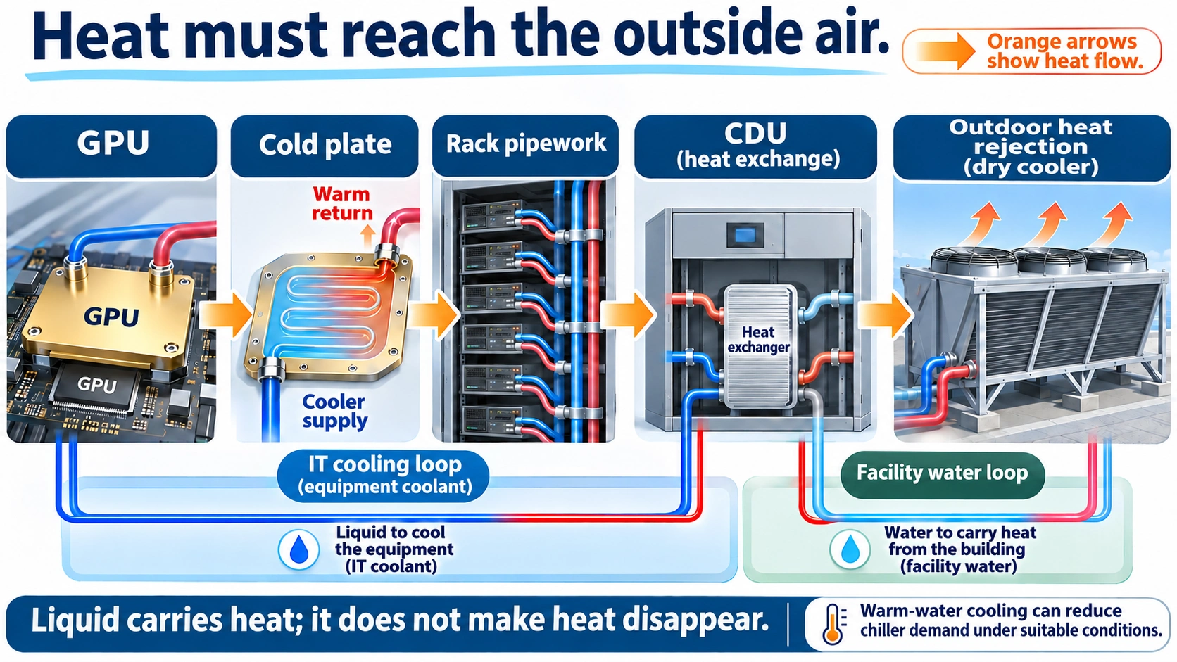
Reading the figure: Orange arrows trace heat, not a continuous stream of the same liquid. A heat exchanger can transfer energy between separate cooling circuits.
Electricity demand reaches beyond the data centre
The IEA's Energy and AI, published in 2025, estimated that all data centres worldwide used about 415 TWh in 2024, roughly 1.5% of global electricity consumption. Its Base Case projected about 945 TWh in 2030 and around 1200 TWh in 2035. These are scenario results from that report, not observed future consumption or AI-only totals. [38][39]
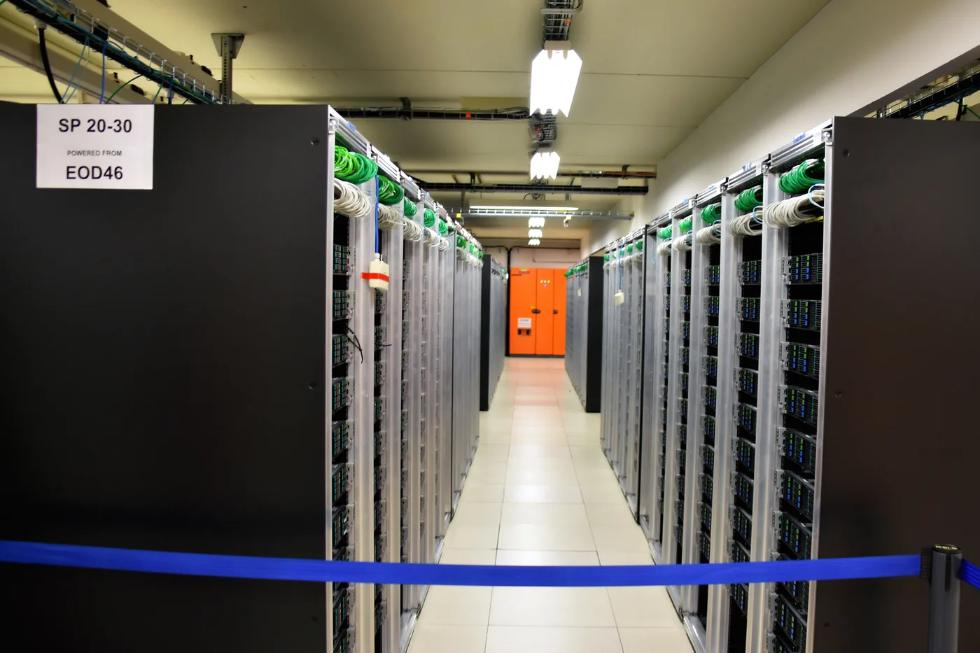
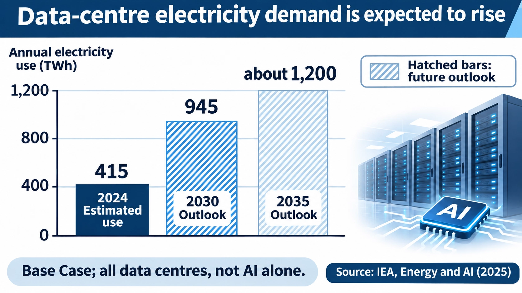
Reading the figure: The 2030 and 2035 bars are forecasts in the 2025 Base Case. The total includes conventional computing as well as AI. Alternative assumptions produce different outcomes.
For scale, the report compared the 2030 total with slightly more than Japan's contemporary electricity consumption. Converting 945 TWh per year into average power gives about 108 GW continuously. That is an annual average, not the same quantity as peak demand.
The IEA expected electricity demand from AI-optimised data centres to more than quadruple by 2030. In its Base Case, accelerated-server electricity demand grew around 30% annually and contributed almost half the net increase in total data-centre demand. [64][39]
Other evidence shows the pressure from different angles:
- Lawrence Berkeley National Laboratory estimated US data-centre use at 176 TWh in 2023, or 4.4% of US electricity, and projected 325-580 TWh in 2028, or 6.7-12.0%. The range reflects uncertainty. [41]
- The IEA's *Electricity 2026* reported US demand growth of 2.1% in 2025 and projected growth near 2% annually to 2030, with data centres accounting for about half the increase. [40]
- Google's 2025 environmental report recorded a 27% rise in data-centre electricity use in 2024. Microsoft's 2025 sustainability reporting put total emissions 23.4% above its 2020 baseline and energy use 168% higher, alongside the expansion of AI and cloud services. These are company-wide or activity-specific reporting measures with different boundaries. [44][45]
A grid connection can take longer than a chip generation
Having generation somewhere on the grid does not guarantee that sufficient power can reach a proposed site. Transmission, substations, transformers, cables and connection studies can become limiting factors.
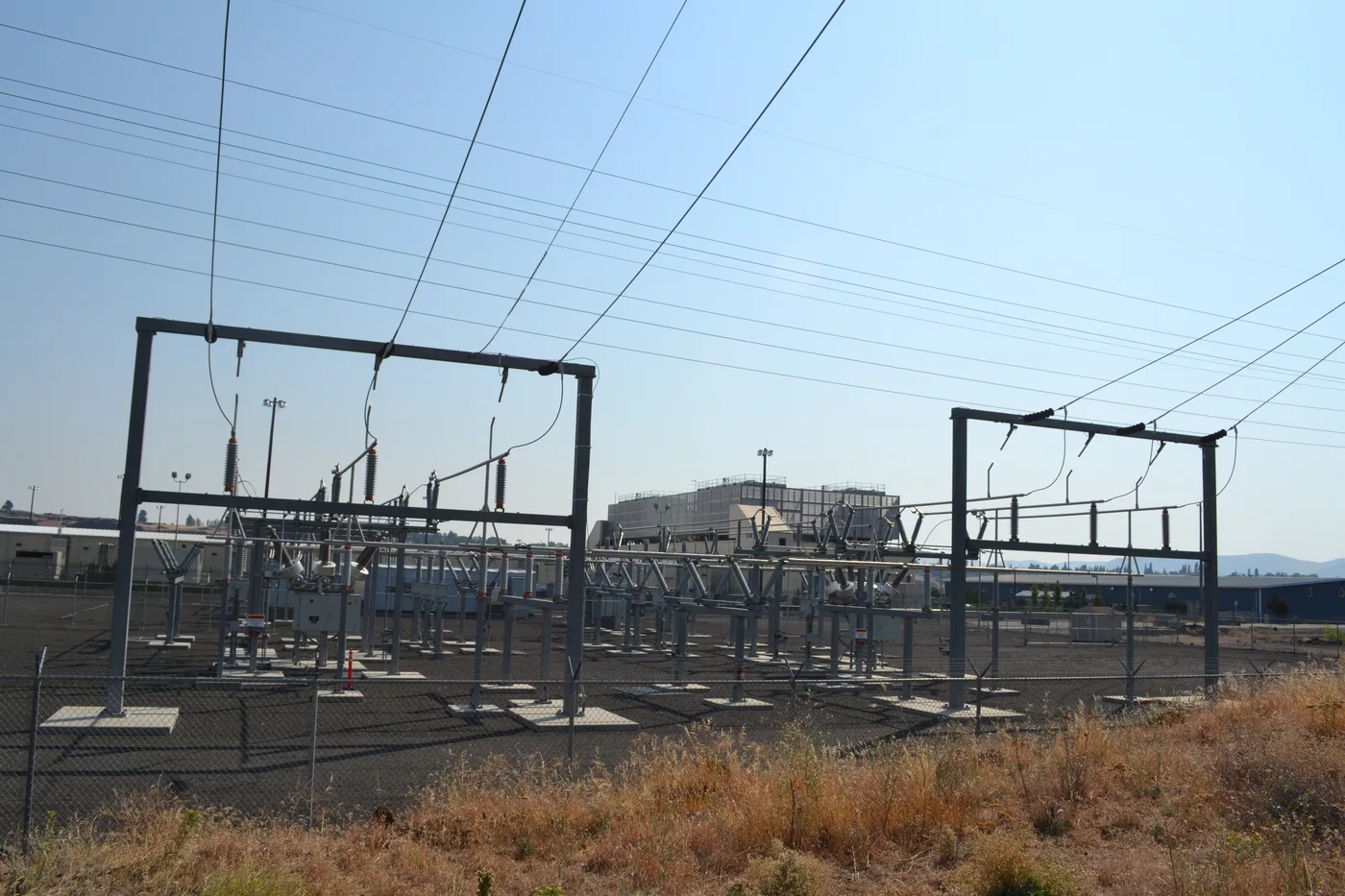
The IEA warned that grid constraints could delay around 20% of planned data-centre projects without action. It described new transmission lines in advanced economies taking four to eight years, important equipment lead times having doubled over three years, and more than 2500 GW of projects waiting for grid connections across categories including generation and large loads. Those queued projects are not all data centres. [38][40]
The timing mismatch is striking: accelerator generations can change in a year or two, while major electrical infrastructure takes much longer. The inference is that power availability can determine where AI capacity is built, even when chips and finance are available.
The Japanese context
Japan's Seventh Strategic Energy Plan, approved in February 2025, anticipated electricity demand returning to growth as digitalisation and decarbonisation progressed. It highlighted data centres and semiconductor factories, and warned that insufficient decarbonised electricity could cost the country investment opportunities. [43]
OCCTO's January 2026 demand outlook projected nationwide peak demand in fiscal 2026 rising by 0.5%. Its individually identified additions from data centres and semiconductor factories contributed 4.20 GW in fiscal 2030 and 7.62 GW in fiscal 2035; the data-centre portion in 2035 was 6.61 GW. Hokkaido and the Tokyo region were particularly prominent. These are forecast additions in the outlook, not total national demand. [42]
The energy plan also identified efficient semiconductors and optical-electrical integration as ways to improve energy use. Power availability is therefore both a constraint on the market and a reason to develop more efficient devices. [43]
Power delivery: distribute high, convert close to the load
There is a smaller version of the grid problem inside the rack. As power rises, distributing it at low voltage requires very large currents.
Electrical power is P = VI. At an assumed 1 MW, distributing at 54 V requires about 18,500 A; at 800 V, about 1250 A. Cable heating is I²R.
Keep delivered power and cable resistance the same and the current falls to roughly 1/15, while resistive loss falls to roughly 1/220. This comparison excludes conversion losses, changes in conductor design and other system effects. It does not mean the facility's total electricity bill falls by a factor of 220.
NVIDIA's 2025 architecture discussion proposed an 800 VDC transition starting in 2027 to support megawatt-scale racks. It argued that conventional 54 V distribution becomes difficult as rack power increases, illustrating the copper burden with as much as 200 kg of busbar material for a 1 MW rack. It also advertised up to 5% end-to-end efficiency improvement in its architecture comparison and 85% more transmitted power for the same conductor size when comparing its 800 VDC approach with the cited 415 VAC arrangement. These are distinct comparisons, not interchangeable efficiency factors. [36]
In the described Kyber concept, a high-ratio converter close to the GPU reduces 800 V to approximately the 12 V intermediate range. Further local regulation supplies the GPU's much lower operating voltage, around 1 V in this explanatory picture. The power circuitry performs that conversion; the GPU's ordinary transistors are not connected directly to 800 V. The architecture is a development direction, not a description of every current data centre. [65]
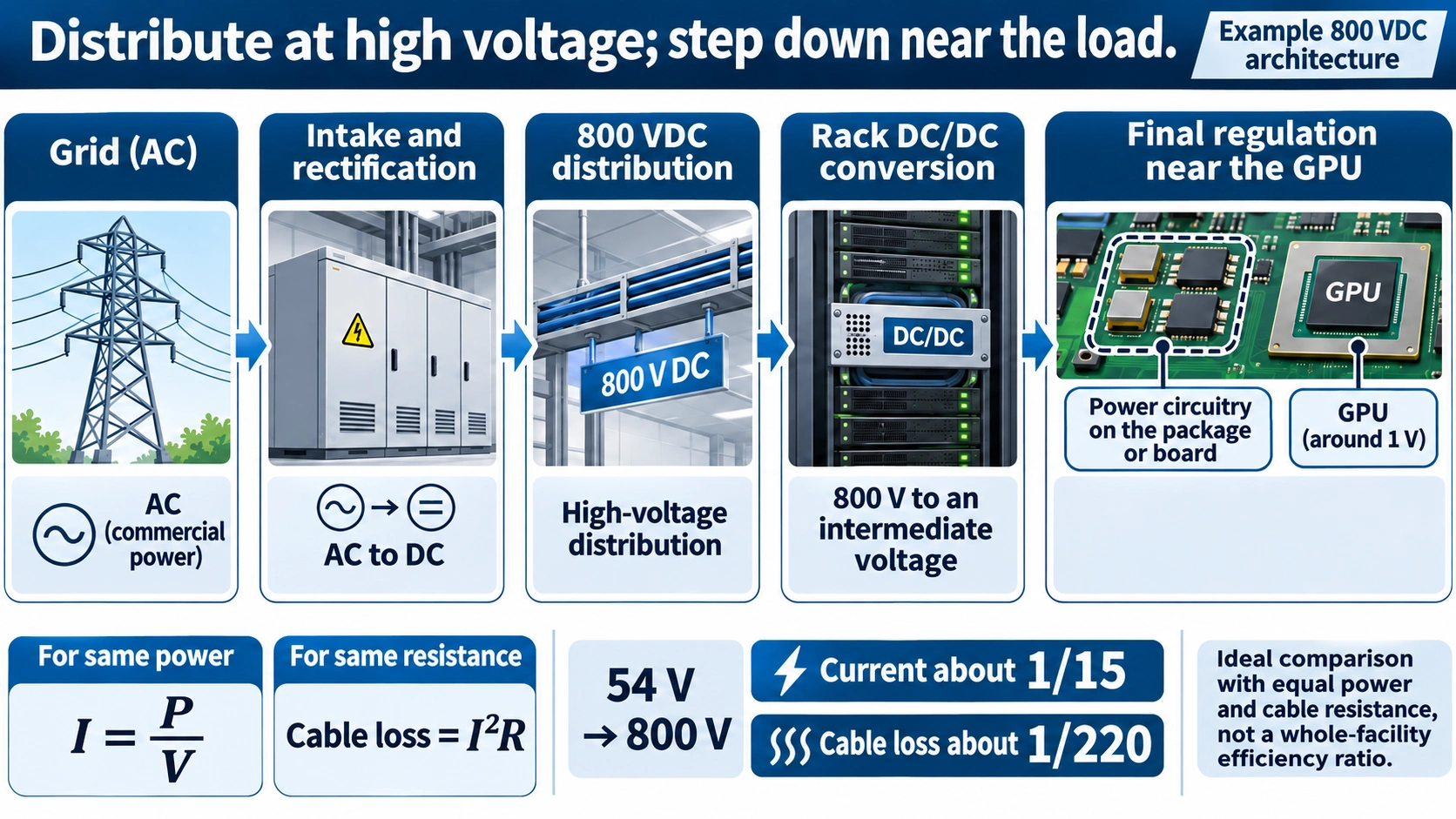
Reading the figure: Track where voltage changes. The cable-loss calculation compares equal power and resistance; practical designs also have to manage converter efficiency, protection, insulation and transient loads.
Four constraints, connected solutions
The preceding sections can be organised into four physical constraints.
| Constraint | What limits progress? | Main responses |
|---|---|---|
| Size | One conventional logic die must fit the practical lithography exposure field | Chiplets and advanced packaging |
| Data supply | Memory bandwidth and transfer energy lag compute growth | HBM, data reuse, lower precision and closer memory/logic integration |
| Heat and power | High device power, concentrated heat and rack supply requirements | Better transistors, backside power, liquid cooling and redesigned distribution |
| Connectivity | Large groups of accelerators must exchange data efficiently | Faster electrical links, network co-design and optical interconnects |
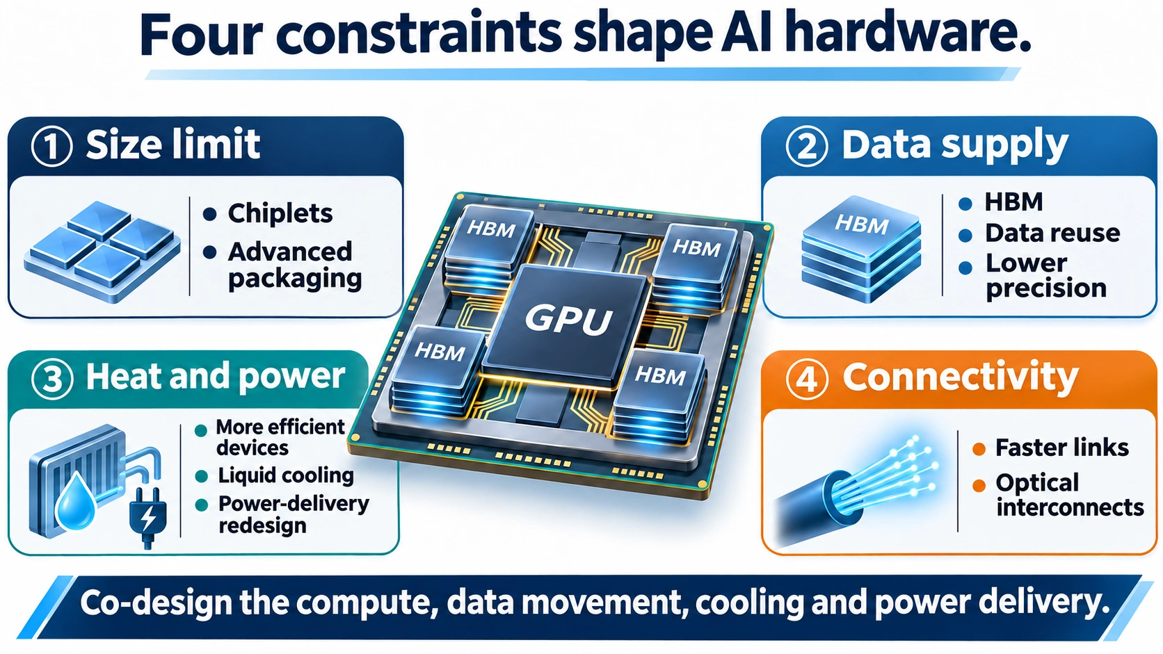
Reading the figure: Faster memory is useful only if the package, cooling and power system support the resulting activity. The four cards represent interacting design problems.
Size: connect dies when one is no longer enough
A lithography system has a maximum exposure field. For conventional large logic dies, that constrains the useful area available in one exposure. Blackwell combines two large dies through a 10 TB/s die-to-die link rather than relying on one still larger monolithic die. [6]
TSMC's CoWoS-S description gives an interposer example of 3.3 reticle areas, around 2700 mm², and points towards CoWoS-L and CoWoS-R for larger integration requirements. The company connected strong demand to generative AI and identified advanced-packaging expansion as an investment priority. [29][53]
ASML reported shipping its first advanced-packaging lithography system in 2025. Packaging is therefore part of the performance problem, not merely a protective box added after the important work is finished. [52]
Devices and wiring: GAA and backside power
The following process developments illustrate efforts to improve energy efficiency, with status tied to the cited announcements:
- TSMC N2 entered volume production in the fourth quarter of 2025, using nanosheet gate-all-around transistors. The company's third-quarter 2026 reporting attributed 8% of wafer revenue to 2 nm. [47][54]
- Intel 18A entered high-volume manufacturing in late 2025. Intel's disclosure described the combination of RibbonFET gate-all-around devices and PowerVia backside power. Any claim of being “first” must specify which technology or combination is being compared. [49]
- TSMC A16 combines nanosheets with Super Power Rail backside power. Relative to N2P, TSMC described 8-10% higher speed at the same voltage or 15-20% lower power at the same speed, with production readiness planned for the second half of 2026. These are alternative comparison conditions, and readiness is not the same as a measured customer-product result. [48]
TSMC reported high-performance computing at 58% of its 2025 revenue, showing why these requirements influence the process roadmap. [53]
Traditionally, power and signal wiring share the multilayer space above the transistors. Narrower wires have greater resistance. Current through resistance produces IR drop, reducing the voltage delivered to the devices.
imec describes the growing difficulty of containing distribution losses as dimensions shrink. Backside power introduces a separate route, with power connections arriving from the back of a thinned wafer. This can ease congestion on the signal side and improve power delivery, although the exact implementation varies. [50]
TSMC's Super Power Rail description emphasises freeing front-side routing for signals and reducing IR drop. The solution depends on transistor processing, wafer thinning, alignment and interconnection working together. [48]
Connectivity: electrical links and optical interfaces
Large models can span thousands of accelerators, making communication part of the computation. In its January 2026 Rubin announcement, NVIDIA described sixth-generation NVLink bandwidth of 3.6 TB/s per GPU and 260 TB/s per rack. Industry groups also published UALink 200G 1.0 in April 2025 and Ultra Ethernet 1.0 in June 2025. Their purposes and topologies differ; they should not be treated as one interchangeable link. [11][66][67]
Electrical connections become harder to operate efficiently as distance, bandwidth and signal-integrity demands grow. Co-packaged optics, or CPO, moves optical interfaces close to switching silicon. NVIDIA's March 2025 announcement claimed 3.5 times greater power efficiency and a fourfold reduction in laser count in its stated network-switch comparison. This is an attributed product comparison, not a blanket result for all optical links. TSMC and Sumitomo Electric were among the named collaborators. [46]
Supply is another constraint
Technical capability is concentrated among a relatively small number of suppliers. NVIDIA's annual report describes dependence on external wafer manufacturing, memory suppliers and advanced packaging, including important operations in Taiwan and South Korea. [51]
ASML is the sole supplier of EUV lithography systems in the cited commercial supply chain, while critical optics depend on Carl Zeiss. Intel's 2025 filing identified a risk that development of 14A could be paused without a sufficiently large external customer commitment. These disclosures illustrate capital intensity and concentration; they do not establish that a particular interruption will occur. [52][49]
Japan's role: materials, manufacturing and packaging
Japan's June 2026 semiconductor and digital-industry strategy called for coordinated development of leading logic from the 2 nm generation onwards, advanced memory including HBM, production ramp-up and the surrounding supply chain. It also treated packaging, substrates and encapsulation materials as foundations for both advanced and established products. [55]
Rapidus announced work on 600 mm-square RDL interposer panels through Rapidus Chiplet Solutions alongside its transistor development. The Resonac-led JOINT3, involving 27 companies, announced a pilot line for 515 × 510 mm organic-interposer panels, planned to operate in 2026. These are specific development programmes and announced schedules. [56][57]
Rectangular panels can use area differently from circular wafers, which becomes attractive as packages grow. Usable yield, patterning, warpage, handling and interconnect quality still determine whether the apparent area advantage becomes an economic benefit.
What remains research rather than a production promise
Some approaches try to change the relationship between computation and data movement more radically.
Analogue in-memory computing: IBM researchers reported a chip with 35 million phase-change-memory devices and energy efficiency up to 12.4 TOPS/W in their study. Stored states participate directly in analogue computation, reducing some transfers, but conversion, accuracy and system integration remain important. [58]
Photonic computation: Lightmatter's research reported optical processing of workloads including ResNet image recognition and BERT language tasks, with results approaching electronic implementations on many studied operations. This is research evidence, not proof that a complete commercial AI system can dispense with electronics. [59]
Vertically stacked transistors: Japan's strategy identifies CFET, stacking complementary n- and p-type devices, among future device directions. It also discusses chiplets, advanced packaging, optical-electrical integration and neuromorphic computing. Their development stages differ, and neither a roadmap nor a research demonstration guarantees a deployment date. [55]
Bring the layers of the system together
| Design question | What AI makes especially important |
|---|---|
| How should arithmetic be organised? | Parallel arrays and specialised execution alongside CPUs |
| How many bits are necessary? | Numerical formats matched to accuracy and workload |
| Where should data sit? | Wide, close interfaces and deliberate reuse |
| How does heat escape? | Package-level thermal design and facility cooling |
| How does power arrive? | Low-loss distribution and local regulation |
| How do processors cooperate? | Die-to-die links, networks and optical interfaces |
AI has not made ordinary computing disappear. It has made the interdependence of these design layers harder to ignore. Better transistors, HBM, TSVs, interposers, power wiring and cooling all contribute to useful throughput.
The next introduction follows how such devices are actually made, from design and masks through wafer fabrication, assembly and test, and maps the companies that perform those jobs.
Check your understanding
Why are GPUs useful for many AI workloads?
Show answer
Many matrix operations offer large numbers of similar calculations that can be carried out in parallel. GPUs organise hardware for throughput, while CPUs remain useful for control, varied tasks and sequential dependencies.
Does a CPU-core count mean the same thing as a CUDA-core count?
Show answer
No. They describe different hardware structures. Counting them does not give a direct speed ratio.
What does the memory wall describe?
Show answer
A mismatch in which compute capability grows faster than the bandwidth supplying it, so data delivery limits useful performance. The cited historical paper summarised compute growth around 3.0 times per two years, versus 1.6 for DRAM bandwidth.
Why can small-batch decoding sit on the sloping part of a roofline?
Show answer
It can perform relatively little arithmetic per weight byte fetched. In the simplified four-bit, one-sequence example, the intensity is about four operations per byte, far below the illustrative 2600-operation crossover.
What are two ways HBM helps?
Show answer
A very wide interface transfers many bits in parallel, while placement close to the processor permits short connections. Stacking provides capacity within the package footprint.
At equal delivered power and cable resistance, what happens when distribution rises from 54 V to 800 V?
Show answer
The ideal current falls to about one fifteenth and resistive cable loss to about one two-hundred-and-twentieth. These are cable comparisons, not whole-facility savings.
Why must the IEA's 2030 electricity figure be labelled as an outlook?
Show answer
The 945 TWh value is a Base Case projection from the 2025 report. It is not a measured future total and includes all data centres, not AI alone.
Why can backside power help a dense chip?
Show answer
It gives power a separate route, reducing competition with signal wiring and helping manage resistance and voltage drop. The benefit depends on the implemented process and layout.
A short glossary
- CPU
- Central processing unit, designed for varied instruction streams and system control as well as parallel work.
- GPU
- Graphics processing unit, now widely used as a high-throughput parallel accelerator.
- Core
- An execution structure; its meaning and complexity depend on the architecture.
- Thread
- A sequence of instructions managed as a unit of execution.
- Cache
- A nearby data store used to reduce access to more distant memory.
- FLOPS
- Floating-point operations per second, with numerical format and counting conventions specified.
- TOPS
- Trillions of operations per second; the operation and precision must be defined.
- TPU
- Google's Tensor Processing Unit family of specialised AI accelerators.
- ASIC
- Application-specific integrated circuit.
- NPU
- Neural processing unit, an AI-oriented engine often integrated into a device platform.
- Inference
- Running a trained model to produce an output.
- Training
- Updating model parameters using data and an optimisation procedure.
- Weight
- A learned model parameter used in computation.
- MAC
- Multiply-accumulate operation.
- Systolic array
- Arithmetic cells that pass and reuse data in a coordinated pattern.
- FP4
- A four-bit floating-point format; exact encoding and scaling depend on the implementation.
- Sparsity
- A property that can allow selected zero or unnecessary operations to be skipped.
- Memory wall
- A performance constraint caused by inadequate data supply relative to compute capability.
- Roofline model
- An upper-bound model combining peak compute throughput with bandwidth and arithmetic intensity.
- Arithmetic intensity
- Operations performed per byte transferred from the memory level being analysed.
- Memory capacity
- The amount of data that can be stored.
- Memory bandwidth
- Data transferred per unit time.
- Token
- A unit of text representation, not necessarily one complete word.
- Batching
- Processing multiple requests or examples together to share work and data.
- HBM
- High-bandwidth memory using vertically connected DRAM stacks.
- TSV
- Through-silicon via, a vertical electrical connection through silicon.
- Interposer
- An intermediate structure connecting dies within a package.
- CoWoS
- TSMC's family of advanced integration and packaging technologies.
- Base die
- The supporting logic/interface die beneath a memory stack.
- PIM
- Processing-in-memory, placing selected computation near or within stored data.
- TDP / board power
- Different specified power measures; their definitions must accompany comparisons.
- Dennard scaling
- Historical scaling relationships linking transistor dimensions, voltage and power density.
- Cold plate
- A heat-transfer structure that carries package heat into a coolant.
- CDU
- Coolant distribution unit; commonly manages circulation and heat exchange between cooling circuits.
- TWh
- Terawatt-hour, a unit of energy equal to one billion kilowatt-hours.
- GW
- Gigawatt, a unit of power equal to one million kilowatts.
- Busbar
- A substantial conductor used to distribute electrical current.
- Reticle field
- The lithography exposure area relevant to conventional die-size constraints.
- Chiplet
- A die designed to be integrated with other dies into a functional package.
- GAA
- Gate-all-around transistor structure.
- Backside power
- Power distribution using the back side of a processed wafer or die.
- IR drop
- Voltage lost as current flows through resistance.
- NVLink
- NVIDIA's interconnect technology family.
- CPO
- Co-packaged optics, integrating optical interfaces close to switching or computing packages.
- EUV
- Extreme-ultraviolet lithography.
- CFET
- Complementary field-effect transistor arrangement with vertically stacked n- and p-type devices.
- Panel-level integration
- Fabricating selected package structures on larger rectangular panels.
Sources and reading notes
The sources below support the device explanations, worked examples and dated industry snapshots in this chapter. Company performance comparisons retain their original attribution and require the stated conditions. Forecasts, targets and research demonstrations are different kinds of evidence from production results. The diagrams are explanatory models; the historical growth graph is schematic and the electricity chart presents the 2025 IEA Base Case.
- NVIDIA — CUDA Programming Guide: Introduction — Read source
- AMD — AMD EPYC 9005 Series Processors — Read source
- NVIDIA — GeForce RTX 5090 — Read source
- N. P. Jouppi et al. (Google) — In-Datacenter Performance Analysis of a Tensor Processing Unit (ISCA 2017) — Read source
- Google — Ironwood: The first Google TPU for the age of inference — Read source
- NVIDIA — NVIDIA Blackwell Architecture — Read source
- NVIDIA — GB200 NVL72 — Read source
- NVIDIA — GB300 NVL72 — Read source
- NVIDIA — Inside the NVIDIA Rubin Platform: Six New Chips, One AI Supercomputer — Read source
- NVIDIA — Vera Rubin NVL72 — Read source
- NVIDIA — NVIDIA Kicks Off the Next Generation of AI With Rubin — Read source
- AMD — AMD Instinct MI355X — Read source
- AMD — AMD Instinct MI400 Series — Read source
- Amazon — Trainium3 UltraServers — Read source
- AWS — AWS Trainium — Read source
- Microsoft — Maia 200: The AI accelerator built for inference — Read source
- Microsoft — Introducing Copilot+ PCs — Read source
- Apple — Apple introduces M4 chip — Read source
- Qualcomm — Snapdragon X2 Elite — Read source
- Epoch AI — Training compute of frontier AI models grows by 4-5x per year — Read source
- A. Gholami et al. — AI and Memory Wall (2024) — Read source
- M. Horowitz — Computing's Energy Problem (ISSCC 2014; author-paper copy) — Read source
- S. Williams, A. Waterman and D. Patterson — Roofline: An Insightful Visual Performance Model (UC Berkeley, 2008) — Read source
- NVIDIA — Mastering LLM Techniques: Inference Optimization — Read source
- JEDEC — JESD270-4 HBM4 Standard — Read source
- SK hynix — SK hynix Completes World-First HBM4 Development and Readies Mass Production — Read source
- Samsung — Samsung Ships Industry-First Commercial HBM4 — Read source
- Micron — HBM4 — Read source
- TSMC — CoWoS® — Read source
- SK hynix — SK hynix Announces 3Q26 Financial Results — Read source
- Samsung — Samsung Electronics Announces Third Quarter 2026 Results — Read source
- NVIDIA — H100 Tensor Core GPU — Read source
- NVIDIA — DGX B200 — Read source
- J. Hennessy and D. Patterson — A New Golden Age for Computer Architecture (Turing Lecture slides, 2018) — Read source
- Vertiv — Understanding direct-to-chip cooling in HPC infrastructure — Read source
- NVIDIA — NVIDIA 800 VDC Architecture Will Power the Next Generation of AI Factories — Read source
- NVIDIA — NVIDIA Vera Rubin POD — Read source
- IEA — Energy and AI: Executive summary — Read source
- IEA — Energy and AI: Energy demand from AI — Read source
- IEA — Electricity 2026: Executive summary — Read source
- Lawrence Berkeley National Laboratory — 2024 United States Data Center Energy Usage Report — Read source
- OCCTO — Electricity demand outlook for fiscal 2026 (Japanese; 21 January 2026) — Read source
- Agency for Natural Resources and Energy, Japan — Seventh Strategic Energy Plan (Japanese; approved 18 February 2025) — Read source
- Google — 2025 Environmental Report — Read source
- Microsoft — 2025 Environmental Sustainability Report — Read source
- NVIDIA — NVIDIA Spectrum-X and Quantum-X Co-Packaged Optics Networking Switches — Read source
- TSMC — 2nm Technology — Read source
- TSMC — A16 Technology — Read source
- Intel (SEC filing) — Form 10-K, fiscal 2025 — Read source
- imec — How to power chips from the backside — Read source
- NVIDIA (SEC filing) — Form 10-K, year ended January 2026 — Read source
- ASML (SEC filing) — Form 20-F, fiscal 2025 — Read source
- TSMC (SEC filing) — Form 20-F, fiscal 2025 — Read source
- TSMC (SEC filing) — Third-quarter 2026 results, Form 6-K — Read source
- METI, Japan — Semiconductor and Digital Industry Strategy (Japanese; June 2026 revision) — Read source
- Rapidus — Analysis centre and Rapidus Chiplet Solutions (11 April 2026) — Read source
- Resonac — JOINT3 panel-level organic-interposer programme (3 September 2025) — Read source
- S. Ambrogio et al. (IBM Research) — An analog-AI chip for energy-efficient speech recognition and transcription (Nature, 2023) — Read source
- Lightmatter researchers — Universal photonic artificial intelligence acceleration (Nature, 2025) — Read source
- WSTS — Spring 2026 semiconductor market forecast — Read source
- SIA — 2026 State of the Industry Report — Read source
- NVIDIA — Financial Results for Fourth Quarter and Fiscal 2026 — Read source
- Samsung — Samsung Develops Industry's First High Bandwidth Memory with AI Processing Power — Read source
- IEA — AI is set to drive surging electricity demand from data centres — Read source
- NVIDIA — Building the 800 VDC Ecosystem for Efficient, Scalable AI Factories — Read source
- UALink Consortium — UALink 200G 1.0 specification announcement (April 2025) — Read source
- Ultra Ethernet Consortium — UEC specification 1.0 launch (11 June 2025) — Read source
- SK hynix — TSMC Technology Symposium 2026 (23 April 2026) — Read source
Evidence map and calculation assumptions
| Topic | Supporting sources | How to interpret it |
|---|---|---|
| CPU/GPU organisation, cores, TPU and accelerator examples | [1–19] | Architectural explanations and dated vendor figures; different formats and comparison conditions |
| Training-compute growth and historical memory wall | [20][21] | Analyses of specified historical periods, not guaranteed future growth |
| Data-movement energy | [22] | Historical illustrative energy figures; the 1536 W thought experiment is this article's calculation |
| Roofline and decoding | [23][24][10] | Upper-bound model; 2600 operations/byte, 0.15%, 15 ms and 67 tokens/s are simplified estimates |
| HBM standards and products | [25–31][68] | Standard parameters, vendor specifications and dated supply expectations are different evidence types |
| Power and cooling | [7][12][32–39] | Die, board and system power are not interchangeable; the heat-flux example assumes area and power |
| Global electricity and grid constraints | [38–41][64] | Estimated history, scenarios and connection constraints; 108 GW is an annual-average conversion |
| Japan's energy outlook and company environmental figures | [42–45] | Forecast peak additions and reported energy/emissions have different units and boundaries |
| 800 VDC | [36][65] | Proposed architecture; current and cable-loss ratios assume equal power and resistance |
| Packaging, processes and backside power | [29][47–50][52–54] | Published process status and targets; performance/power alternatives use stated comparison conditions |
| Networks and supply concentration | [11][46][49][51][52][66][67] | Product claims, standards announcements and disclosed business risks |
| Japan's industrial programmes and research directions | [55–59][63][68] | Plans and demonstrations are not guaranteed production schedules |
| Market and revenue context | [60–62] | Spring 2026 forecast and dated company reporting, not a new full-year market result |
Matrix-operation counts, raw weight-storage sizes, power-law comparisons and energy conversions are calculations made here from explicitly stated inputs. Reference numbering matches the companion Japanese edition, allowing readers to trace the evidence across both versions.
English edition authored on 3 November 2026 from the Japanese edition dated 2 November 2026. Product figures are attributed announcement or reporting snapshots, not directly comparable benchmarks. Forecasts and research results are identified separately. Illustrations are conceptual and not to scale. Photograph credits and licences accompany each image.
Original explanatory illustrations generated with OpenAI Image Gen for this English edition. Third-party photographs retain their stated licences; image credits accompany each photograph.