COMPANY PROFILE / NANOTECHNOLOGY
ASM International
Tools and processes for atomic layer deposition (ALD), which builds films one atomic layer at a time, used to form the layers of 2nm-generation gate-all-around transistors
ASM International (ASM) is a Dutch semiconductor equipment maker. It appears in a nanotechnology series because it supplies, for volume chip production, the tools and processes for atomic layer deposition (ALD), a way to build up films one atomic layer at a time. The company describes itself as the leader in ALD equipment (its own estimate; this profile does not adopt market-share figures), and its annual report says ALD is its largest product line, accounting for more than half of equipment sales. Revenue in 2025 was €3.17 billion, driven by investment in leading-edge logic and foundry (2nm gate-all-around, or GAA, transistors). ASM calls itself a "materials discovery company" and says its strengths are precursor chemistry (the chemicals that supply the film's atoms), plasma, and atomic-scale process technology. This profile focuses on ALD tools and processes (epitaxy, CMP and vertical furnaces are mentioned only briefly), and sets out what primary sources confirm and what they do not.
- ASM International in 30 seconds, and where it stands in nanotechnology
- The logo and how the name is written
- Where the company sits in the nanotechnology field
- Scale
- Resources committed to nanotechnology
- What it has done so far
- What comes next
- What the company is aiming for in nanotechnology
- Map of partnerships in nanotechnology
- Technologies, products and services
- The risks this company carries
- Glossary, references and claim-to-source audit
1. ASM International in 30 seconds, and where it stands in nanotechnology
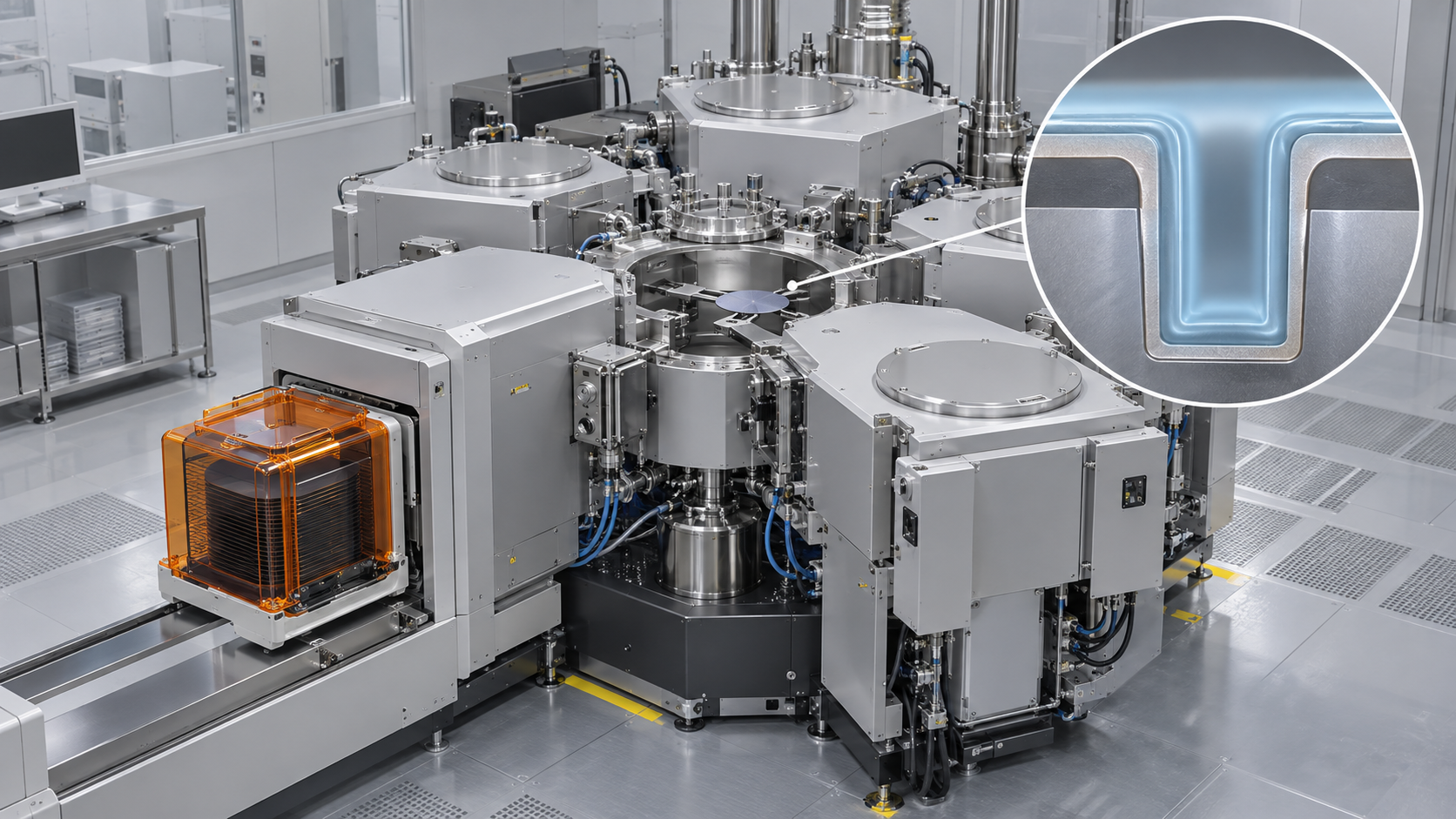
ASM is "a company that sells the tool that lays down films one atomic layer at a time, together with the chemistry and conditions (the recipe) for those films" Our calculation. ALD builds a film by pulsing precursor gases in turn, purging with inert gas between pulses, and relying on saturating surface reactions to form one layer per cycle (ASM's web page) Sourced. Two things matter for complex three-dimensional structures like GAA: the film coats any surface relief evenly (conformality), and thickness is set in units of atomic layers. But the documents reviewed give no performance numbers for the ALD tools (film uniformity, defects, throughput). The company's "market share" and "market size" figures are its own estimates, and this profile does not adopt them Not yet confirmed.
2. The logo and how the name is written

A note on names: the company is ASM International N.V., known as ASM (formerly also "ASMI"). It is a different company from the lithography-tool maker ASML. ASM's annual report says it began a joint venture with Philips in the mid-1980s to develop lithography technology (now known as ASML) and sold its share in 1988. ASMPT, established in Hong Kong (back-end equipment), is a company that ASM founded in the past and in which it held a 24.65% interest at the end of 2025, but it is a separate company. The logo image was taken from the company's official website.
Official website: https://www.asm.com/3. Where the company sits in the nanotechnology field
4. Scale
ASM has annual revenue of about €3.2 billion and also has businesses beyond ALD (epitaxy, vertical furnaces and others), so this profile gives company-wide figures briefly and adds the ALD-related figures in text. The fiscal year is the calendar year, amounts are in euros, and the accounting standard is IFRS.
| Measure (€ million) | 2025 | 2024 |
|---|---|---|
| Revenue | 3,173.2 | 2,932.7 |
| of which equipment revenue | 2,457.5 | 2,303.3 |
| of which Spares & Services revenue | 715.7 | 629.4 |
| Gross profit (gross margin) | 1,643.6 (51.8%) | 1,481.4 (50.5%) |
| Operating result | 938.0 | 802.1 |
| Net R&D expenses (gross R&D spending was €512 million in 2025) | 409.0 | 369.8 |
| Capital expenditure | 218 | 168 |
| Employees (year end) | 4,519 | 4,558 |
In 2025 ALD was the largest product line, clearly more than half of equipment sales, and grew by a double-digit percentage year on year (ALD alone is not disclosed in amounts; company statement) Sourced. By region, Asia was 80.2% of revenue (€2,544.1 million), the United States 15.3% and Europe 4.5%. Equipment sales to China were more than 30% of total revenue in 2025. The five largest customers accounted for 53.6% of revenue and the ten largest for 72.3%, and two customers each exceeded 10% (names are not given) Sourced. In the first half of 2026, revenue was €1,865.6 million (+11%; +20% at constant currency), gross margin 52.6% and adjusted operating result €616.4 million (33.0% margin). Of equipment sales, logic/foundry was 77%, memory 15% and power/analog/wafer 8% Sourced.
Sales, profit and unit shipments for ALD tools are not given as separate figures in the documents reviewed. The annual report gives the relative size of product lines only in words ("ALD is the largest, more than half of equipment sales"). The annual report and investor materials also contain "market size", "market share" and "expansion of the served market" figures, but their basis is the company's own estimates or outside research firms, and this profile does not adopt them Not yet confirmed.
5. Resources committed to nanotechnology
| Resource | What primary sources confirm | Status |
|---|---|---|
| People | 4,519 employees company-wide (end of 2025) and 4,908 (FTE) at the end of June 2026. 27% of employees work in R&D. The company has 8 R&D centers worldwide: corporate R&D in Helsinki (Finland; precursor chemistry) and Leuven (Belgium; materials application and device evaluation), and product development in Almere (Netherlands; vertical furnaces), Phoenix (U.S.; thermal ALD and epitaxy), Hwaseong (Korea; PEALD), Tama (Japan; PECVD and PEALD) and Italy (SiC epitaxy) | Sourced |
| Money (R&D and capital expenditure) | Gross R&D spending was €512 million in 2025 (+9% on 2024) and net R&D expenses €409.0 million. Adjusted net R&D expenses for the first half of 2026 were €209.9 million. Capital expenditure was €218 million in 2025, and the company guides to €150 to 250 million a year in years with infrastructure expansion (company outlook). R&D and capex for ALD alone are not disclosed | Sourced / partly undisclosed |
| Acquisitions, investments, joint ventures, divestments | The company says the acquisition of ASM Microchemistry (Microchemistry Oy, Helsinki) in 1999 and ASM Genitech Korea in 2004 laid the foundation for its ALD position. It acquired LPE (SiC epitaxy) in 2022 and Axus Technology (Chandler, U.S.; CMP equipment) in December 2025 (net cash of €81 million for Axus, plus a €100 million earn-out for LPE). It holds 24.65% of ASMPT | Sourced |
| Universities, research institutes, public funding | A partnership with imec (Belgium) since 1990, with an on-site presence since 1994, and a sixth strategic partnership agreement in January 2026. The ALD Center of Excellence with the University of Helsinki, formed and funded by ASM. Participation in the Semiconductor Research Corporation (SRC) Nanomanufacturing Processes program. A four-year collaboration with Eindhoven University of Technology (TU/e), signed in 2024, and a collaboration with TU Delft. University research through funding from the Dutch NWO (TTW domain), and projects supported by Flanders' VLAIO. Individual grant amounts could not be confirmed | Sourced / amounts not confirmed |
Status of key products and facilities
| Product / facility | Content (company statements) | Stage | Date / source |
|---|---|---|---|
| ALD tool range | Thermal ALD and PEALD tools (Pulsar, EmerALD, Synergis, the XP8 DCM, QCM, JQCM and Magma, and others). The XP4 and XP8 are 300 mm single-wafer platforms; the XP8 takes up to 16 chambers | Supplied | 2025 and 2026 (References 1, 5) |
| Mo ALD (molybdenum ALD) | First applications shipped at the 2nm node. The company says adoption has not been as fast as anticipated a few years ago but remains a longer-term opportunity. In July 2026 it reported wins at the 1.4nm node | Shipped for volume use (2nm). 1.4nm is Not yet confirmed | March and July 2026 (References 1, 3) |
| New R&D center in Scottsdale (U.S.) | Expands ALD and epitaxy R&D. Announced in 2023 | Under construction. Opening planned for early 2027 (Not yet confirmed) | March 2026 (Reference 1) |
| Manufacturing and innovation center in Dongtan (Korea) | A manufacturing and R&D site. The next phase was completed in 2025. With its Singapore manufacturing site, the company says it supports growth well into the next decade | Operating (described as opened) | March 2026 (Reference 1) |
| New headquarters and R&D facility in Almere (Netherlands) | Global headquarters, an R&D center, a training hub and part of product development. Several hundred million euros of investment is expected over the coming years | Planned (intention announced in December 2025; Not yet confirmed) | March 2026 (Reference 1) |
6. What it has done so far
| When | What happened | Why it matters |
|---|---|---|
| 1968 | ASM founded in the Netherlands. ASM America was established in 1976 (the base of its epitaxy technology), and ASM Japan has developed plasma CVD products since 1982 | The starting point as a deposition-equipment company |
| 1980s | In the mid-1980s it began a joint venture with Philips on lithography technology (now ASML), and sold its share in 1988 | Lithography and deposition go separate ways |
| 1999 and 2004 | Acquired ASM Microchemistry (Helsinki) and ASM Genitech Korea | The base in ALD precursor chemistry and PEALD |
| 2007 | The company says its Pulsar ALD tool became the first system used in volume manufacturing of devices with a hafnium-based high-k gate dielectric at the 45nm node | A milestone for ALD entering volume production (company statement) |
| 2011 | The company says it played an important role in the move to 22nm (from planar to FinFET transistors) | Meeting three-dimensional transistors |
| 2024 to 2025 | 2nm GAA entered volume manufacturing and ALD sales grew. Revenue reached a record €3.17 billion in 2025 | The ramp of GAA drives results |
| December 2025 | Acquired Axus Technology (CMP equipment). Announced its intention to build a new headquarters and R&D facility in Almere | Adjacent technology and wider R&D |
| January 2026 | Signed its sixth strategic partnership agreement with imec | Continuing a collaboration of more than 30 years |
| 28 July 2026 | Second-quarter revenue reached a record €1.003 billion. The company said it had won Mo ALD business at the 1.4nm node | Groundwork for the next generation (1.4nm) |
7. What comes next
The primary sources also contain the following policies and plans Not yet confirmed.
- The 1.4nm node: the July 2026 announcement says the 1.4nm node is on track for its first meaningful contribution in the second half of 2026, that ASM has gained share in both ALD and epitaxy, and that it has won Mo ALD business there. The annual report expects transistor layers to be about 60% of all ALD layers at 1.4nm (50% at 2nm) (company outlook)
- Memory: DRAM for high-bandwidth memory (HBM) led in 2026, and another DRAM customer selected ASM's epitaxy solution. The annual report calls the next DRAM nodes a major opportunity
- Facilities: the Scottsdale (U.S.) R&D center is planned to open in early 2027. The Almere headquarters and R&D facility is expected to take several hundred million euros of investment. The company says its current manufacturing capacity is enough for its 2030 revenue target and beyond
- Capex guidance: €150 to 250 million a year in years with infrastructure expansion (company outlook)
Sales, profit, unit shipments and R&D for ALD alone / numerical performance of the ALD tools (film uniformity, defect density, throughput) / the names of customers that adopted ASM tools at the 1.4nm node / the total purchase prices of Axus and LPE (only the €81 million net cash for Axus is given) / individual grant amounts for universities and public bodies. Either the documents reviewed (the annual report, results announcements, interim report and web pages) do not state them, or we could not check the original text.
8. What the company is aiming for in nanotechnology
This section separates what the company says it aims for from what we read into it. Inference marks our interpretation of primary sources.
| What can be read | Primary basis | Type |
|---|---|---|
| Enter each device generation change with new materials and atomic-scale processes | In July 2026 the CEO called the company a "materials discovery company" and said precursor chemistry and atomic-scale process technology enable leading-edge logic and HBM. The annual report describes depositing new materials with better control and conformality | Sourced (company description) |
| Grow its opportunity with the number of ALD layers in generations such as GAA | The annual report says GAA needs additional ALD and epitaxy steps and that ALD intensity rises. It says the ALD portfolio grew from three to four layers in 2003 to more than 80 today | Sourced (company description) |
| Win adoption by pairing materials and tools in the next nodes (1.4nm, the next DRAM generation) | July 2026: wins in Mo ALD at 1.4nm. It also aims to gain share in DRAM in both ALD and epitaxy | Sourced (company description) / Inference (whether adoption continues) |
| Place R&D close to customers and research institutes | Leuven is on imec's premises, Helsinki is for precursor chemistry, and facilities are expanding in Scottsdale, Dongtan and Almere | Sourced (where sites are) / Inference (whether closeness is the aim) |
The reading that "ASM values being adopted for the combination of precursor, tool and recipe more than for tool performance alone" rests on wording in the annual report. It says most new process applications are customer specific and come out of joint development programs (JDPs) with customers, and that these programs run from the node now in production to N+2 and beyond Sourced. It also divides roles between sites: Helsinki for precursor chemistry, and Leuven for materials application and device evaluation Sourced. From this we read that holding everything from chemicals (precursors) through the tool to evaluation in devices is, in our view, the reason ASM gets adopted. However, ASM's documents do not give the reasons for individual adoptions or a comparison with competitors. Whether precursors are made in-house or bought was also not confirmed in the documents reviewed Not yet confirmed.
9. Map of partnerships in nanotechnology
The main ASM partnerships that the documents reviewed confirm are imec (since 1990, with a site on its Leuven premises), the University of Helsinki (the ALD Center of Excellence), universities and research consortia in the Netherlands, Belgium and the United States, and joint development programs with customers (JDPs) Sourced. ASM writes that its JDPs run from the current node to N+2 and beyond, but the documents do not name individual customers or say which customer adopted which tool. The suppliers of precursors, and any individual contracts ASM has with chemical makers, are not in the documents reviewed Not yet confirmed.
10. Technologies, products and services
This profile concentrates on ALD tools and processes (epitaxy, PECVD, vertical furnaces and CMP are touched on only briefly). Performance numbers are the company's own statements, and conditions are given with them. Numbers such as film uniformity for the ALD tools are not in the documents reviewed.
| Category | What official material says | Conditions, scale, source |
|---|---|---|
| The ALD method | Precursor and reactant are pulsed in turn, with an inert-gas purge between pulses, to build a film one atomic layer at a time. Saturating surface reactions (self-limiting) make thickness a matter of the number of cycles. The film is even over surfaces with a lot of relief. Nanolaminates (stacks of different materials) can be made | Company statement (web page). No conditions given |
| Thermal ALD and PEALD | Thermal ALD drives the reaction with heat. PEALD uses an RF plasma to supply the reaction energy, allowing lower temperatures for uses with a low thermal budget | Company statement (web page). Same precursors are used |
| Tools (platforms and products) | 300 mm single-wafer platforms: the XP4 (up to four process modules), the XP8 (up to 16 chambers) and the XP8E (up to six dual or quad chamber modules). ALD products include the Pulsar (high-k), EmerALD (metal and dielectric), Synergis (thermal ALD), and the XP8 DCM, QCM and JQCM (PEALD) and Magma | Company statement (annual report, web page). No throughput figures given |
| Main uses | High-k metal gates (GAA), dipole layers, work-function metals, spacers, high-aspect-ratio gap fill, underlayers for EUV lithography, metal ALD, selective ALD (ASD) and MIM capacitors | Company statement (annual report). Mo ALD and ASD entered volume production at the 2nm node, the company says (March 2026) |
| Number of processes | The ALD portfolio grew from three to four layers in 2003 to more than 80 layers today. The company says it has developed reference processes for more than 70% of the elements cited in the ALD literature | Company statement (annual report). Not independently verified |
| Spares and services | Outcome-based services (guaranteed performance and availability). A target of more than half of spares and services sales by 2030 | Spares and services revenue was €715.7 million in 2025. The target is a company plan |
What matters in ALD is precursor chemistry and the substrate surface. According to ASM's annual report, the Helsinki site works on precursor chemistry for new ALD materials and the Leuven site on applying the materials and evaluating them in devices Sourced. For metal ALD, the company says it developed a surface clean that removes impurities and moisture before deposition, integrated on the same platform so the vacuum is not broken Sourced. For metal oxides it developed a reactor that can deposit five, six or even seven elements. The documents reviewed do not say which precursors (chemicals) the ALD films are made from.
In a GAA transistor the gate completely surrounds the channel (stacked nanosheets), so a film must coat evenly deep inside the gaps. The annual report names the high-k dielectric, dipole layers for multiple threshold voltages and work-function metals as GAA transistor layers, and expects them to be about 60% of all ALD layers at 1.4nm (50% at 2nm) (company outlook) Not yet confirmed. For interconnect and contacts, the company says Mo ALD will in time replace more of the tungsten and copper layers, and also says adoption is slower than anticipated. The documents reviewed give no figures for the reasons (resistivity, barrier thickness and so on). Because ALD adds roughly one atomic layer per cycle, more layers mean more cycles and more time, which is a general challenge (a general explanation, not a figure from the company's documents). The company's emphasis on multi-chamber configurations (up to 16 chambers on the XP8) is probably aimed at securing throughput Our calculation.
11. The risks this company carries
| Risk | What it involves | Type |
|---|---|---|
| Customer concentration | In 2025 the five largest customers were 53.6% of revenue and the ten largest 72.3%, with two customers each above 10%. Results depend on the investment plans of a few leading-edge logic makers | Sourced |
| China and export controls | In 2025 equipment sales to China were more than 30% of total revenue (mainly mature logic and foundry). The annual report says possible future export-control measures could further limit the available market in China. The documents reviewed do not describe a specific new rule coming into force (the stage of any proposal, adoption or enforcement has to be checked separately) | Sourced (company statement) |
| Demand swings | In 2025 power/analog/wafer fell and China memory normalized, and fourth-quarter revenue was down 7% year on year at constant currency. Results follow swings in chip capital spending | Sourced |
| Slower adoption of new materials and uses | The company says Mo ALD adoption has not been as fast as anticipated a few years ago. Volume production at the 1.4nm node follows customers' plans (2027 to 2028) and could slip | Sourced (company statement) / Not yet confirmed |
| Reliance on the company's own estimates | Market share and the expansion of its served market are the company's estimates, and the documents reviewed show no third-party verification. They are hard to check from outside | Sourced |
| Burden of sites and investment | New facilities in Scottsdale, Dongtan and Almere raise capital expenditure (guidance of €150 to 250 million a year). Almere is described as "several hundred million euros". If demand falls short of expectations, the burden could grow | Sourced / Inference |
| Hiring skilled people | Headcount rose by 389 (FTE) in the first half of 2026 and overall attrition rose to 15% (14% in the first half of 2025). Recruiting and retention could become a burden as the business expands | Sourced / Inference (hiring and retention burden) |
12. Glossary
- ALD (atomic layer deposition)
- A method that pulses precursor and reactant in turn to build a film one layer at a time. See our explainer on atomic layer deposition.
- PEALD
- Plasma-enhanced ALD. A plasma supplies the reaction energy, so films can be made at lower temperatures.
- Precursor
- The chemical that supplies a film's material. In ALD it is delivered as a gas that reacts with the substrate surface.
- Self-limiting reaction
- A reaction that stops once the surface is saturated. It is why thickness depends on the number of cycles.
- GAA (gate-all-around)
- A transistor whose gate surrounds stacked nanosheet channels on all sides. See our explainer on nanoscale transistors.
- High-k / metal gate
- A gate insulator with a high dielectric constant, and a metal gate electrode. Typical layers made by ALD.
- Dipole layer
- An extremely thin layer used to tune a transistor's threshold voltage (for devices with several threshold voltages).
- Selective ALD (ASD)
- Growing a film only on certain surfaces. Intended to widen the alignment margin.
- Epitaxy (Epi)
- Growing a crystalline film that follows the crystal underneath. Another main product line of ASM.
- JDP (joint development program)
- A program with a customer to develop tools and processes for volume production.
13. References
- ASM International Annual Report 2025 (published 12 March 2026). Business overview, revenue and profit, the ALD and epitaxy businesses, R&D, partnerships, capital expenditure and customer concentration. https://www.asm.com/media/3skhiimk/asm-2025-annual-report.pdf
- ASM International Press release "ASM reports Q4 and full-year 2025 results" (3 March 2026). Equipment and spares & services revenue for 2025, and orders. https://www.asm.com/media/yvxbavwe/20260303-asm-reports-q4-and-full-year-2025-results.pdf
- ASM International Press release "ASM reports second quarter 2026 results" (28 July 2026). Second-quarter results, outlook, and remarks on the 1.4nm node. https://www.asm.com/media/y0mkxj21/20260728-asm-reports-second-quarter-2026-results.pdf
- ASM International Interim Report 2026 (first half of 2026). Revenue, R&D expenses and headcount for the first half. https://www.asm.com/media/4s2bztwz/asm-statutory-interim-report-2026.pdf
- ASM International Company website, "ALD". The ALD principle, thermal ALD and PEALD, and the list of tools. https://www.asm.com/our-technology-products/ald
- ASM International Company website (source of the logo image). https://www.asm.com/media/uotnslj4/asm-logo2022_rgb_innovationpurple-1.png

14. Claim-to-source audit
| Claim in the text | Type | Source |
|---|---|---|
| ASM International N.V. is a Dutch company headquartered in Almere, listed on Euronext Amsterdam (ASM) and in the AEX index. Fiscal year ends 31 December | Sourced | Reference 1 https://www.asm.com/media/3skhiimk/asm-2025-annual-report.pdf Reference 3 https://www.asm.com/media/y0mkxj21/20260728-asm-reports-second-quarter-2026-results.pdf |
| 2025: revenue of €3,173.2 million (2024: €2,932.7 million), equipment revenue of €2,457.5 million (€2,303.3 million), spares & services revenue of €715.7 million (€629.4 million), gross profit of €1,643.6 million (51.8% margin), operating result of €938.0 million (€802.1 million), net R&D expenses of €409.0 million (€369.8 million) | Sourced | Reference 1 https://www.asm.com/media/3skhiimk/asm-2025-annual-report.pdf Reference 2 https://www.asm.com/media/yvxbavwe/20260303-asm-reports-q4-and-full-year-2025-results.pdf |
| Gross R&D spending of €512 million (+9%), capital expenditure of €218 million (2024: €168 million), 4,519 employees (2024: 4,558). 27% of employees work in R&D. 8 R&D centers worldwide | Sourced | Reference 1 https://www.asm.com/media/3skhiimk/asm-2025-annual-report.pdf |
| ALD is the largest product line and more than half of equipment sales. ALD alone is not disclosed. It grew by a double-digit percentage in 2025 | Sourced | Company statement. Reference 1 https://www.asm.com/media/3skhiimk/asm-2025-annual-report.pdf |
| By region: Asia 80.2% (€2,544.1 million), the United States 15.3%, Europe 4.5%. Equipment sales to China were above 30% of revenue. The five largest customers 53.6%, the ten largest 72.3%, and two customers above 10% | Sourced | Reference 1 https://www.asm.com/media/3skhiimk/asm-2025-annual-report.pdf Reference 2 https://www.asm.com/media/yvxbavwe/20260303-asm-reports-q4-and-full-year-2025-results.pdf |
| First half of 2026: revenue of €1,865.6 million (+11%; +20% at constant currency), equipment of €1,470.0 million, spares & services of €395.6 million, gross margin of 52.6%, adjusted operating result of €616.4 million (33.0%), adjusted net R&D expenses of €209.9 million. Equipment sales: logic/foundry 77%, memory 15%, power/analog/wafer and other 8%. 4,908 employees (FTE) at the end of June 2026 | Sourced | Reference 4 https://www.asm.com/media/4s2bztwz/asm-statutory-interim-report-2026.pdf |
| Second quarter of 2026: revenue of €1,003.1 million. Q3 outlook of €1,100 million (±5%, at constant currency), with the second half more than 20% above the first. 2027 revenue expected to exceed the top of the €3.7 to 4.6 billion target range | Not yet confirmed | The company's outlook. Reference 3 https://www.asm.com/media/y0mkxj21/20260728-asm-reports-second-quarter-2026-results.pdf |
| 2030 revenue of €5.7 billion or more (annual growth of at least 12%), operating margin above 30%. Spares & services to grow more than 12% a year, with outcome-based services above half | Not yet confirmed | Company target. Reference 1 https://www.asm.com/media/3skhiimk/asm-2025-annual-report.pdf |
| The ALD principle: precursor and reactant pulsed in turn with an inert-gas purge; self-limiting surface reactions set thickness by cycle count; even coverage of relief; nanolaminates possible. PEALD uses RF plasma to supply reaction energy | Sourced | Company statement. Reference 5 https://www.asm.com/our-technology-products/ald |
| The list of ASM ALD tools (EmerALD XP, Pulsar, Synergis, XP8 DCM/QCM/JQCM/Magma and others) and the configuration of the XP4, XP8 and XP8E | Sourced | Company statement. Reference 1 https://www.asm.com/media/3skhiimk/asm-2025-annual-report.pdf Reference 5 https://www.asm.com/our-technology-products/ald |
| Mo ALD and ASD entered volume production at the 2nm node. Mo ALD wins at the 1.4nm node. Mo ALD adoption slower than anticipated. 1.4nm pilot-line investment in H2 2026 and volume production in 2027 to 2028 (customers' plans) | Not yet confirmed | Company statement. Reference 1 https://www.asm.com/media/3skhiimk/asm-2025-annual-report.pdf Reference 2 https://www.asm.com/media/yvxbavwe/20260303-asm-reports-q4-and-full-year-2025-results.pdf Reference 3 https://www.asm.com/media/y0mkxj21/20260728-asm-reports-second-quarter-2026-results.pdf |
| GAA transistor layers: high-k, dipole layers and work-function metals. About 60% of ALD layers at 1.4nm (50% at 2nm) | Not yet confirmed | Company outlook. Reference 1 https://www.asm.com/media/3skhiimk/asm-2025-annual-report.pdf |
| The ALD portfolio grew from three to four layers in 2003 to more than 80; reference processes for more than 70% of elements in the ALD literature; Pulsar first used in volume manufacturing of hafnium-based high-k gates at 45nm in 2007; a role in the move to 22nm in 2011 | Sourced | Company statement; not independently verified. Reference 1 https://www.asm.com/media/3skhiimk/asm-2025-annual-report.pdf |
| Founded in 1968; ASM America 1976, ASM Japan 1982. Joint venture with Philips in the mid-1980s on lithography (now ASML), share sold in 1988. ASM Microchemistry in 1999, ASM Genitech Korea in 2004, LPE in 2022 and Axus in December 2025. 24.65% of ASMPT | Sourced | Reference 1 https://www.asm.com/media/3skhiimk/asm-2025-annual-report.pdf |
| Net cash of €81 million for Axus (and a €100 million earn-out for LPE: €181 million of M&A-related cash) | Sourced | Reference 1 https://www.asm.com/media/3skhiimk/asm-2025-annual-report.pdf |
| A partnership with imec since 1990 (on site since 1994) and a sixth strategic partnership agreement in January 2026. The ALD Center of Excellence with the University of Helsinki. The SRC Nanomanufacturing Processes program. A four-year collaboration with TU/e (2024) and one with TU Delft. Projects through NWO (TTW) and VLAIO. JDPs with customers (to N+2 and beyond) | Sourced | Reference 1 https://www.asm.com/media/3skhiimk/asm-2025-annual-report.pdf |
| The Scottsdale R&D center is under construction and planned to open in early 2027. The Dongtan (Korea) center completed its next phase in 2025. A new Almere headquarters and R&D facility with several hundred million euros of investment (intention announced December 2025). Capex guidance of €150 to 250 million a year | Not yet confirmed | Company plan. Reference 1 https://www.asm.com/media/3skhiimk/asm-2025-annual-report.pdf |
| Possible future export-control measures could further limit the available market in China | Sourced | The company's risk statement. No specific rule coming into force is described. Reference 1 https://www.asm.com/media/3skhiimk/asm-2025-annual-report.pdf |
| Headcount rose by 389 (FTE) in the first half of 2026, and attrition rose to 15% (14% in the first half of 2025) | Sourced | Reference 4 https://www.asm.com/media/4s2bztwz/asm-statutory-interim-report-2026.pdf |
| Sales, profit, shipments and R&D for ALD alone; numerical performance of the ALD tools; names of 1.4nm customers; individual grant amounts | Not yet confirmed | Not stated in the documents reviewed, so not confirmed. We do not estimate them (outlook). |
| The company's market-share and market-size figures are not adopted here | Our calculation | This article's policy, because their basis is the company's own estimates or outside research firms. |
| The logo image is from the company website | Sourced | Reference 6 https://www.asm.com/media/uotnslj4/asm-logo2022_rgb_innovationpurple-1.png |
| The four-type grouping and the example company names | Our calculation | Our own grouping. Company names are examples from companies covered in this series. |
| "ALD adds roughly one atomic layer per cycle, so more layers mean more cycles and time" and "multi-chamber configurations are aimed at throughput" | Our calculation | Commentary: a general explanation and this article's interpretation, not figures from the company's documents. |
| The reading that ASM values being adopted for the combination of precursor, tool and recipe | Inference | Our interpretation of the description of JDPs and of the division of roles between Helsinki and Leuven. Reference 1 https://www.asm.com/media/3skhiimk/asm-2025-annual-report.pdf |
| The reading that recruiting and retention could become a burden as the business expands | Inference | Our interpretation of the headcount rise and the higher attrition in the interim report. Reference 4 https://www.asm.com/media/4s2bztwz/asm-statutory-interim-report-2026.pdf |
| The reading that placing R&D near customers and research institutes is the aim | Inference | Our interpretation of where the sites are (for example, Leuven is on imec's premises). Reference 1 https://www.asm.com/media/3skhiimk/asm-2025-annual-report.pdf |
Last updated 9 October 2026 / Troy Technical
Figures in this article come from ASM International's Annual Report 2025, its results announcements (March and July 2026), its interim report for the first half of 2026, and its website. No research-firm estimates or press-based figures have been used. Market share and market size are the company's own estimates and are not adopted here. The company's outlooks, plans and targets are its own statements and have not been independently verified. Passages marked "Inference" are this article's interpretation of primary sources, not statements made by the company.