COMPANY PROFILE / NANOTECHNOLOGY
ASML
A lithography-equipment maker that prints nanometer-scale circuit patterns with 13.5 nm EUV light: 48 EUV systems and about €11.6 billion of EUV system sales in 2025
ASML is a Dutch company that builds the lithography machines that print circuits onto chips with light. It belongs in a nanotechnology series because it manufactures, as production equipment, the light source, optics and positioning that let chipmakers shrink line widths in nanometer steps. It describes itself as the only manufacturer of extreme ultraviolet (EUV) lithography systems (the company's own statement). Its website gives the following manufacturer's stated values: EUV light has a wavelength of 13.5 nm, and resolution is 13 nm on systems with a numerical aperture (NA) of 0.33 and 8 nm on systems with an NA of 0.55 (High NA). The light-sensitive materials (resists), masks and pellicles used in exposure are not ASML products, so making real patterns depends on surrounding materials and on joint development with research institutes. This profile takes a nanofabrication view (how resolution is set, the light source and mirrors, and the link to resists), and sets out what primary sources confirm and what they do not.
- ASML in 30 seconds, and where it stands in nanotechnology
- The logo and how the name is written
- Where the company sits in the nanotechnology field
- Scale
- Resources committed to nanotechnology
- What it has done so far
- What comes next
- What the company is aiming for in nanotechnology
- Map of partnerships in nanotechnology
- Technologies, products and services
- The risks this company carries
- Glossary, references and claim-to-source audit
1. ASML in 30 seconds, and where it stands in nanotechnology
ASML is "a company that sells the light and optics that draw nanometer-scale patterns, as machines". It is not a nanomaterials producer Our calculation. Resolution is set by the wavelength (λ), the numerical aperture (NA) and a process-side coefficient (k1), in the Rayleigh equation CD = k1 × λ/NA (ASML's technology page) Sourced. The machine supplies λ and NA, while k1 is lowered together with resists, masks, etching and other surrounding steps. So the performance of ASML's machines cannot be separated from progress in resists and other materials. What conditions the company's stated resolutions (13 nm and 8 nm) assume, and how far they are used in actual chip production, cannot be confirmed from the documents reviewed Not yet confirmed.
2. The logo and how the name is written

A note on names: the company is ASML Holding N.V., known as ASML. The name comes from its original name, ASM Lithography (the company's history page). ASM International (deposition equipment and atomic layer deposition) is a separate listed company and has its own profile in this series. ASML's history page says Philips and ASMI (Advanced Semiconductor Materials International, now ASM International) created the new company, and ASM International's annual report says it started the lithography joint venture with Philips in the mid-1980s and sold its share in 1988. The logo is the shape used in the company's own site logo, saved as a standalone SVG file.
Official website: https://www.asml.com/3. Where the company sits in the nanotechnology field
4. Scale
ASML is a large company, so this profile gives company-wide figures briefly and concentrates on the EUV system figures that matter for nanofabrication. The fiscal year is the calendar year, amounts are in euros, and the accounts are under US GAAP.
| Measure (€ million) | 2025 | 2024 |
|---|---|---|
| Net sales | 32,667.3 | 28,262.9 |
| of which system sales | 24,474.3 | 21,768.7 |
| of which service and field option sales | 8,193.0 | 6,494.2 |
| Income from operations | 11,301.4 | 9,022.6 |
| Net income | 9,609.4 | 7,571.6 |
| R&D costs | 4,698.8 | 4,303.7 |
| Purchase of property, plant and equipment (capex) | 1,573.6 | 2,067.2 |
| Employees (end of year) | 44,175 (headcount) / more than 44,000 (FTE) | 43,395 (headcount) |
EUV system figures (sales by technology)
| Technology | 2024 | 2025 | First half of 2026 |
|---|---|---|---|
| EUV 0.33 NA (NXE) | 42 units / 7,856.4 | 44 units / 10,445.8 | 29 units / 6,708.5 |
| EUV 0.55 NA (EXE, High NA) | 2 units / 465.0 | 4 units / 1,156.9 | 3 units / 1,188.9 |
| EUV total | 44 units / 8,321.4 Our calculation | 48 units / 11,602.7 Our calculation | 32 units / 7,897.4 Our calculation |
| ArF immersion (DUV, 193 nm) | 129 units / 9,667.0 | 131 units / 10,311.4 | 40 units / 3,331.7 |
| Total system sales (all technologies) | 583 units / 21,768.7 | 535 units / 24,474.3 | 274 units / 12,844.2 |
Each cell reads "units / amount (€ million)". Units are systems recognized in sales, which can differ from units shipped. The EUV total is our sum of the NXE and EXE units and amounts.
EUV system sales in 2025 (€11.60 billion) were about 47% of system sales and about 36% of total net sales Our calculation (11,602.7 ÷ 24,474.3 and 11,602.7 ÷ 32,667.3, rounded). The documents reviewed give no profit or gross profit for EUV alone. In 2025 one customer accounted for 23.9% of net sales, and four customers each exceeded 10%, together making up 61.2% (customer names are not given) Sourced.
The units above are systems recognized in sales. The company's CFO letter in the annual report explains that field upgrades of NXE:3800E systems already in customers' fabs moved a substantial part of EUV system revenue into installed base revenue (service and field option sales). The full EUV-related revenue may therefore be larger than the system sales above, but the documents reviewed do not let us separate that amount, and we do not estimate it Not yet confirmed.
5. Resources committed to nanotechnology
| Resource | What primary sources confirm | Status |
|---|---|---|
| People | 44,175 employees company-wide (headcount, end of 2025): 23,707 in the Netherlands, 8,242 in the United States and 4,548 in Taiwan. The July 2026 press release says "more than 44,500 (FTE)". Manufacturing (assembly and testing) takes place in Veldhoven, Eindhoven, Oirschot, Berlin, Wilton, San Diego, Pyeongtaek, Linkou and Tainan. Headcount for EUV alone is not disclosed | Sourced / partly undisclosed |
| Money (R&D and capital expenditure) | R&D costs were €4.70 billion in 2025 (14.4% of sales). In 2025 the main work was developing the NXE:3800E and NXE:3800F, developing the High NA EXE systems, and developing DUV and metrology and inspection. R&D for the first half of 2026 was €2.5 billion (the company's wording; €1.8 billion a year earlier), including EXE-related work and the NXE:3800F and NXE:4200G platforms. Purchases of property, plant and equipment were €1.57 billion in 2025. R&D and capex for EUV alone are not disclosed | Sourced / partly undisclosed |
| Acquisitions, investments, joint ventures, divestments | A 24.9% interest in Carl Zeiss SMT Holding was acquired on 29 June 2017 (equity method); Zeiss SMT is the sole supplier of the optics. Cymer (San Diego, light sources) was acquired in 2013. Loan agreements with Carl Zeiss SMT of up to €1 billion each were signed in 2021 and 2024, and further loans were made in 2025. Also, in 2025, a €1.30 billion investment in Mistral (an AI company, not directly related to nanofabrication) | Sourced |
| Universities, research institutes, public funding | Key partners named include the technical universities of Delft, Eindhoven and Twente, ARCNL (Advanced Research Center for Nanolithography), TNO, CEA-Leti, Fraunhofer and imec. In March 2025 ASML signed a five-year strategic partnership with imec. In the United States it names the University of California system, Stanford, MIT and others. It takes part in research projects subsidized by the EU and its member states (Horizon Europe and the European Chips Act are mentioned). Individual grant names and amounts could not be confirmed in the documents reviewed | Sourced / grant details not confirmed |
Status of key products and facilities
| Product / facility | Specification (manufacturer's stated values) | Stage | Date / source |
|---|---|---|---|
| TWINSCAN NXE:3800E (EUV, 0.33 NA) | 13.5 nm wavelength, 13 nm resolution, at least 220 wafers per hour (at a dose of 30 mJ/cm²). The annual report calls this a 37% improvement over the NXE:3600D | Shipped (shipped at full specification in 2025; fielded systems also upgraded) | 2025 (References 1, 5) |
| TWINSCAN EXE:5200B (High NA, 0.55 NA) | 13.5 nm wavelength, 8 nm resolution, at least 175 wafers per hour (at a dose of 50 mJ/cm²). The annual report calls this 60% higher productivity than the EXE:5000 | Shipped (first system in early April 2025, released at full specification to the first customer). Start of high-volume use expected in 2027 (Not yet confirmed) | 2025 (References 1, 6) |
| TWINSCAN EXE:5000 (early High NA system) | 13.5 nm wavelength, 8 nm resolution, at least 110 wafers per hour (at a dose of 50 mJ/cm²). Operating in the joint lab with imec | Operating (joint research lab, opened June 2024) | 3 June 2024 (References 11, 15) |
| NXE:3800F and NXE:4200G (next 0.33 NA systems) | Specifications are not given in the documents reviewed | In development (listed in the breakdown of first-half 2026 R&D) | July 2026 (Reference 3) |
| EUV (0.33 NA) production capacity | About 65 systems in 2026. The plan is to add 30% in 2027, and ASML is investigating another 30% for 2028 | Not yet confirmed (company plan) | 15 July 2026 (Reference 2) |
The two throughput figures are stated at different doses (30 mJ/cm² and 50 mJ/cm²), so the numbers cannot simply be set side by side. What a dose means is explained in Section 10.
6. What it has done so far
| When | What happened | Why it matters |
|---|---|---|
| 1984 | Philips and ASMI created ASM Lithography to develop lithography systems, and launched the PAS 2000 stepper. A partnership with Carl Zeiss was established in 1986 | The pattern of building optics with an outside specialist |
| 2010 | Shipped a prototype EUV tool (TWINSCAN NXE:3100) to the research facility of an Asian chipmaker | EUV hardware reaches a customer |
| 2013 | Acquired Cymer (San Diego), a maker of lithography light sources, and shipped the second-generation NXE:3300 | Brings EUV source development in-house |
| 2016 to 2017 | In 2016 customers began ordering the production-ready NXE:3400. On 29 June 2017 ASML acquired a 24.9% interest in Carl Zeiss SMT Holding | Tighter ties with the optics supplier |
| 31 May 2019 | License agreement with Mitsui Chemicals for the EUV pellicle business (a thin membrane that protects the mask from dust). Mitsui Chemicals said ASML is the only manufacturer to have developed EUV pellicles for commercial use | Leaves a mask-adjacent material to a materials company |
| 2020 | EUV moved into high-volume manufacturing, and shipments reached 100 EUV systems (company history) | A track record in volume production builds up |
| 2023 | Shipped the first next-generation EUV system with a 0.55 numerical aperture (EXE) | The move to High NA |
| 3 June 2024 | Opened the High NA EUV Lithography Lab in Veldhoven jointly with imec. The EXE:5000 printed 10 nm dense lines (20 nm pitch) on metal oxide resists for the first time, according to the announcement | A hub for joint work on tools, resists and masks |
| 2025 | Shipped the NXE:3800E at full specification, and the first EXE:5200B in early April. Signed a five-year strategic partnership with imec in March | Both 0.33 NA and 0.55 NA moved forward |
| 15 July 2026 | Raised the 2026 sales outlook to €43 to 45 billion (the annual report of February 2026 had €34 to 39 billion) | An outlook reflecting strong EUV and DUV demand |
7. What comes next
The primary sources also contain the following policies and plans Not yet confirmed.
- EUV product roadmap: the annual report says the roadmap is meant to drive affordable scaling to 2030 and beyond. The EXE (High NA) platform is designed to share as much as possible with the NXE, and the stated ultimate goal is a common platform early in the next decade
- DUV immersion capacity: about 130 systems in 2026, with a plan to add 30% in 2027 and an investigation of another 30% in 2028
- Next update: the next Capital Markets Day is on 10 June 2027, when longer-term views will be updated
- Export controls and capacity: EUV systems need export licenses under Dutch, U.S. and other laws, and the company writes that changes in controls may affect sales volume, mix and timing
Profit, R&D and headcount for EUV alone / the names and unit counts of EXE (High NA) customers / the specifications and launch timing of the NXE:3800F and NXE:4200G / a split of 2026 EUV sales between NXE and EXE / the size of the Dutch government's "Beethoven" project and any individual public funding amounts received by ASML. Either the documents reviewed (the 20-F, the 6-K, website pages and the joint releases) do not state them, or we could not check the original text.
8. What the company is aiming for in nanotechnology
This section separates what the company says it aims for from what we read into it. Inference marks our interpretation of primary sources.
| What can be read | Primary basis | Type |
|---|---|---|
| Use EUV to replace several exposures with one and simplify the process | The annual report describes the shift from complex multi-patterning to single patterning with EUV, one exposure per layer, which cuts the number of masks and process steps and improves yield | Sourced (company description) |
| Use High NA to widen the room for shrinking | It says EXE lets customers extend their shrink roadmap and minimize double or triple patterning. The website says it is designed to enable multiple future nodes, starting at the 2 nm Logic node | Sourced (company description) |
| Improve resolution on both the optics (wavelength, NA) and the process and computation (k1) | The website sets out the three terms of the resolution equation and gives 0.25 as the physical limit of k1. It describes lowering k1 through computational lithography such as OPC | Sourced |
| Raise performance together with resists, masks and other surrounding materials and with research institutes | The joint release with imec says that imec, with its supplier network, prepared the patterning ecosystem around the tool: resist and underlayer materials, photomasks, metrology and inspection, and more | Sourced (description of the collaboration) / Inference (reading of ASML's intent) |
The reading that "ASML treats progress on the materials side as part of what its tools are worth" rests on the joint release with imec of June 2024. The release says that, alongside readying the tool, imec prepared the surrounding patterning environment, including advanced resist and underlayer materials, photomasks, metrology and inspection techniques, OPC, and integrated patterning and etch techniques, and it cites the printing of 10 nm lines (20 nm pitch) on metal oxide resists as a result Sourced. In 2019, Mitsui Chemicals also announced a license from ASML for the EUV pellicle business, with ASML continuing to develop the technology Sourced. From these we read ASML as putting weight on building out the supply chain of surrounding materials and components, and not only on selling tools. However, we found no ASML document that says this. Where resists are sourced, and what amounts ASML pays or receives from materials companies, are not disclosed Not yet confirmed.
9. Map of partnerships in nanotechnology
The main ASML partnerships that the documents reviewed confirm are Carl Zeiss SMT for optics (supply and equity), imec (the High NA joint lab and a five-year partnership), Mitsui Chemicals (the EUV pellicle license) and Cymer (light sources; acquired and operated independently) Sourced. In May 2024 Mitsui Chemicals announced production facilities at its Iwakuni-Ohtake Works for a pellicle that uses carbon nanotubes (CNTs) as the membrane, for High NA and high-output EUV (annual capacity of 5,000 sheets, with construction expected to finish in December 2025; the company's announcement). That release does not say whether the CNT pellicle is ASML technology, and we could not confirm it Not yet confirmed. The supplier of EUV resists, and any individual contracts ASML has with materials companies, are not in the documents reviewed.
10. Technologies, products and services
ASML provides lithography systems at the core, plus metrology and inspection, software and servicing. Performance numbers are the company's own statements, and conditions are given with them.
| Category | What official material says | Conditions, scale, source |
|---|---|---|
| EUV lithography (NXE, 0.33 NA) | 13.5 nm wavelength; 13 nm resolution. Said to print the critical layers of 7 nm, 5 nm and 3 nm nodes. The NXE:3800E is for volume production of 2 nm Logic and leading-edge DRAM | Manufacturer's stated value (website). NXE:3800E: at least 220 wafers per hour at a 30 mJ/cm² dose |
| High NA EUV (EXE, 0.55 NA) | 13.5 nm wavelength; 8 nm resolution. Intended for volume production of sub-2 nm Logic and leading-edge DRAM | Manufacturer's stated value. EXE:5200B: at least 175 wafers per hour at a 50 mJ/cm² dose |
| DUV immersion (NXT) | ArF laser (193 nm). A layer of water between lens and wafer raises the NA, up to 1.35. Can be used with EUV on different layers of the same chip | Website and annual report. 131 units / €10.31 billion in 2025 (as recognized in sales) |
| DUV (ArF dry, KrF, i-line) | Wavelengths of 193 nm, 248 nm and 365 nm. For a wide range of nodes and uses | Annual report |
| Metrology and inspection | Optical and electron-beam systems used to assess pattern quality and control exposure conditions | 208 units / €0.82 billion in 2025 (as recognized in sales) |
| Computational lithography | Simulation to optimize mask patterns and exposure conditions (OPC and others). In 2025 it enhanced its High NA solutions, including source, mask and wavefront co-optimization | Annual report |
| Servicing and upgrades (installed base management) | Servicing of installed systems and performance upgrades | €8.19 billion in 2025 (25.1% of sales) |
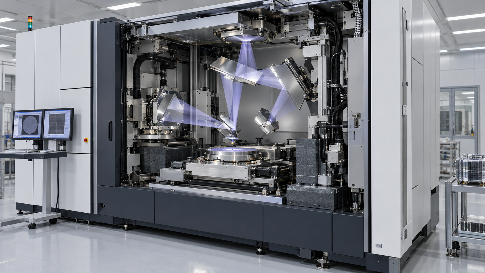
The light source runs on molten tin. According to the website, droplets of molten tin about 25 µm across are ejected at 70 meters per second, flattened by a weak laser pulse, then vaporized by a stronger pulse into a plasma that emits 13.5 nm light. This repeats 50,000 times a second Sourced. EUV cannot use lenses, because most materials absorb EUV light, so the system uses multilayer mirrors in a vacuum. Each mirror has more than 100 layers, the largest are about 1 meter across, and the surface is described as smooth down to tens of picometers Sourced. The layer materials and the allowed density of film defects are not in the documents reviewed.
The other key is the resist. The resolution equation is about optics, but printing 10 nm-scale patterns depends on how the light-sensitive film responds. The website gives throughput at a dose of 30 mJ/cm² for the NXE:3800E and 50 mJ/cm² for the EXE:5200B (dose is the amount of light delivered to the resist). An EUV photon carries about 91.8 eV (E = hc/λ with λ = 13.5 nm), so 30 mJ/cm² is about 20 photons per square nanometer and 50 mJ/cm² about 34 Our calculation (photons arriving at the film; the number absorbed depends on the film's absorption). A 10 nm square then receives roughly 2,000 to 3,400 photons, and the general physics is that random variation in photon count (shot noise) feeds straight into roughness of the printed line. The joint release with imec reports 10 nm dense lines printed on metal oxide resists. The documents reviewed do not describe the resist materials in detail or explain why the two doses differ. Because the conditions differ, the throughput figures of the two systems cannot be set side by side to rank them.
Further, the pellicle that shields the mask from dust must be a thin film that EUV light can pass through. For a CNT-membrane pellicle, Mitsui Chemicals states targets of at least 92% EUV transmittance and light resistance for exposure power above 1 kW (the company's announcement; Not yet confirmed).
11. The risks this company carries
| Risk | What it involves | Type |
|---|---|---|
| Customer concentration | In 2025 four customers each exceeded 10% of net sales, totaling 61.2%; the largest was 23.9% and the top two together 38.0%. A change in one customer's investment plans has a large effect | Sourced |
| A single supplier of optics | Lenses, mirrors, illuminators and collectors come only from Carl Zeiss SMT under an exclusive arrangement. If it cannot maintain or raise output, ASML may be unable to fill orders. The 20-F says that if Zeiss SMT ended supply or could not produce for a prolonged period, ASML would effectively cease to be able to conduct its business | Sourced |
| Export controls and trade measures | EUV systems and some DUV immersion systems need export licenses under Dutch, U.S. and other laws. On 15 January 2025 the Netherlands widened its licensing to cover some metrology and inspection systems. In November 2025 the EU added certain Dutch national controls to the EU control list, extending the license requirement to all member states (ASML says this changed nothing for it, since those immersion products already needed a Dutch license). The U.S. Commerce Department's Affiliates Rule (50%-owned entities), introduced on 1 October 2025, is suspended until 10 November 2026. Customers in China were 29.1% of 2025 net sales (36.1% in 2024) | Sourced (stages shown: in force / suspended) |
| Controls on critical materials | In 2025 China introduced rare earth export controls, suspended for one year until 10 November 2026 under a U.S.-China trade agreement. ASML reviewed the impact on the magnets in its systems and reports no material impact on customers to date | Sourced (suspended) |
| Demand swings and capacity investment | If customers cut capex, sales and profit fall; if capacity is raised and demand does not follow, the 20-F says the result could be losses on those investments. The 2026 plan of about 65 EUV systems and a further 30% in 2027 assumes demand | Sourced / plan: Not yet confirmed |
| Geopolitics (Taiwan and elsewhere) | The 20-F says several of its facilities, supply chain partners and customers are in Taiwan, and that changes in the region's political situation could affect its business (4,548 employees are in Taiwan) | Sourced (company's statement) |
| Uncertainty in technology progress | High NA is expected to enter high-volume use in 2027, but adoption by each customer and the readiness of surrounding items such as resists and masks cannot be checked from outside | Not yet confirmed |
12. Glossary
- Lithography
- The step that prints a circuit pattern onto a light-sensitive film on the wafer. See our explainer on lithography and EUV.
- EUV / DUV
- EUV is extreme ultraviolet light (13.5 nm); DUV is deep ultraviolet (193 nm for ArF, 248 nm for KrF).
- NA (numerical aperture) / High NA
- A measure of how well the optics gather light. EUV tools exist at 0.33 NA and at the 0.55 NA "High NA".
- Rayleigh equation (CD = k1 × λ/NA)
- Gives the resolution (smallest feature, CD). λ is wavelength and k1 a process coefficient with a physical limit of 0.25 (ASML's explanation).
- Resolution (CD)
- The smallest feature that can be printed. The 13 nm and 8 nm here are ASML's stated values, and the k1 and other conditions behind them are not given on the website.
- Resist
- A film whose properties change with light and that forms the basis of the pattern. See our explainer on resists and photomasks.
- Pellicle
- A thin membrane that protects the mask (reticle) from dust. For EUV it must let the light through.
- Immersion
- Filling the gap between lens and wafer with water so the NA can exceed 1.
- Throughput (wafers per hour)
- Wafers processed per hour. Read it together with conditions such as the dose.
- Dose (mJ/cm²)
- The energy of light delivered to the resist per square centimeter.
- Multi-patterning
- Making one layer's pattern through several exposures and etches. EUV aims to replace this with a single exposure.
- OPC (optical proximity correction)
- Computation that corrects, on the mask side, for the distortion of a pattern caused by light diffraction.
13. References
- ASML Form 20-F for the year ended 31 December 2025 (filed 25 February 2026; includes Annual Report 2025). Business overview, EUV system sales and units, R&D, headcount, customer concentration, export controls, the relationship with Carl Zeiss SMT, and partners. https://www.sec.gov/Archives/edgar/data/937966/000162828026011378/asml-20251231.htm
- ASML Press release attached to Form 6-K, "ASML reports €9.3 billion total net sales and €2.9 billion net income in Q2 2026" (15 July 2026). Second-quarter results, the 2026 outlook, and EUV and DUV capacity plans. https://www.sec.gov/Archives/edgar/data/937966/000162828026048235/pressreleasefinancialresul.htm
- ASML Statutory Interim Report 2026 (first half of 2026; attached to the same 6-K). Sales by technology (EXE and NXE units and amounts) and the content of R&D. https://www.sec.gov/Archives/edgar/data/937966/000162828026048235/statutoryinterimreport20.htm
- ASML Company website, "EUV lithography systems". Resolution, NA and light source of the NXE and EXE systems. https://www.asml.com/en/products/euv-lithography-systems
- ASML Company website, "TWINSCAN NXE:3800E". Wavelength, resolution, NA and throughput (at a 30 mJ/cm² dose). https://www.asml.com/en/products/euv-lithography-systems/twinscan-nxe-3800e
- ASML Company website, "TWINSCAN EXE:5200B". Wavelength, resolution, NA and throughput (at a 50 mJ/cm² dose). https://www.asml.com/en/products/euv-lithography-systems/twinscan-exe-5200b
- ASML Company website, "Light and lasers". The EUV source (molten tin droplets and lasers) and the wavelengths and smallest features of each generation. https://www.asml.com/en/technology/lithography-principles/light-and-lasers
- ASML Company website, "Lenses & mirrors". EUV multilayer mirrors, surface smoothness and NA. https://www.asml.com/en/technology/lithography-principles/lenses-and-mirrors
- ASML Company website, "The Rayleigh criterion". The resolution equation CD = k1 × λ/NA and the physical limit of k1 (0.25). https://www.asml.com/en/technology/lithography-principles/rayleigh-criterion
- ASML Company website, "History". Founding in 1984, successive EUV systems, the Cymer acquisition and the first High NA shipment. https://www.asml.com/en/company/about-asml/history
- imec (jointly with ASML) Press release "ASML and imec open joint High NA EUV Lithography Lab" (3 June 2024). Opening of the joint lab and 10 nm lines on metal oxide resists. https://www.imec-int.com/en/press/asml-and-imec-open-joint-high-na-euv-lithography-lab-offering-early-development-platform
- Mitsui Chemicals News release "ASML and Mitsui Chemicals Sign License Agreement for EUV pellicle business" (31 May 2019). License of the EUV pellicle business from ASML. https://jp.mitsuichemicals.com/en/release/2019/2019_0531_01/index.htm
- Mitsui Chemicals News release "Mitsui Chemicals Sets up Production Facilities for CNT Pellicles to Be Used in Next-Gen EUV Lithography" (28 May 2024). Production facilities for CNT pellicles. https://jp.mitsuichemicals.com/en/release/2024/2024_0528_1/index.htm
- ASML Company website (source of the logo; the logo shapes in the site's logo SVG were saved as a standalone SVG file). https://www.asml.com/images/icons/asml-logo.svg
- ASML Company website, "TWINSCAN EXE:5000". Wavelength, resolution, NA and throughput (at a 50 mJ/cm² dose). https://www.asml.com/en/products/euv-lithography-systems/twinscan-exe-5000
- ASM International Annual Report 2025 (published 12 March 2026). Its account of its history (the mid-1980s lithography joint venture and the sale of its share in 1988). https://www.asm.com/media/3skhiimk/asm-2025-annual-report.pdf

14. Claim-to-source audit
| Claim in the text | Type | Source |
|---|---|---|
| ASML Holding N.V. is a Dutch company headquartered in Veldhoven and listed on Euronext Amsterdam and Nasdaq (ASML) | Sourced | The company's own documents. Reference 1 https://www.sec.gov/Archives/edgar/data/937966/000162828026011378/asml-20251231.htm Reference 2 https://www.sec.gov/Archives/edgar/data/937966/000162828026048235/pressreleasefinancialresul.htm |
| 2025 net sales of €32,667.3 million (2024: €28,262.9 million), system sales of €24,474.3 million, service and field option sales of €8,193.0 million, income from operations of €11,301.4 million, net income of €9,609.4 million, R&D costs of €4,698.8 million (14.4% of sales), purchases of property, plant and equipment of €1,573.6 million | Sourced | Reference 1 https://www.sec.gov/Archives/edgar/data/937966/000162828026011378/asml-20251231.htm |
| Employees: 44,175 (headcount) and more than 44,000 (FTE) at the end of 2025; 23,707 in the Netherlands, 8,242 in the United States, 4,548 in Taiwan. More than 44,500 (FTE) as of July 2026 | Sourced | Reference 1 https://www.sec.gov/Archives/edgar/data/937966/000162828026011378/asml-20251231.htm Reference 2 https://www.sec.gov/Archives/edgar/data/937966/000162828026048235/pressreleasefinancialresul.htm |
| Sales by technology: 2025 EXE 4 units / €1,156.9 million, NXE 44 / €10,445.8 million, ArF immersion 131 / €10,311.4 million, metrology and inspection 208 / €824.6 million, total 535 / €24,474.3 million. 2024 EXE 2 / €465.0 million, NXE 42 / €7,856.4 million. Units are as recognized in sales | Sourced | Reference 1 https://www.sec.gov/Archives/edgar/data/937966/000162828026011378/asml-20251231.htm |
| First half of 2026: EXE 3 units / €1,188.9 million, NXE 29 / €6,708.5 million, ArF immersion 40 / €3,331.7 million, total 274 / €12,844.2 million (first half of 2025: EXE 1 / €273.8 million, NXE 24 / €5,593.2 million) | Sourced | Reference 3 https://www.sec.gov/Archives/edgar/data/937966/000162828026048235/statutoryinterimreport20.htm |
| EUV totals: 2025 48 units / €11,602.7 million, 2024 44 / €8,321.4 million, first half of 2026 32 / €7,897.4 million. About 47% of system sales and about 36% of net sales | Our calculation | Our calculation, adding NXE and EXE; 11,602.7 ÷ 24,474.3 = 47.4% and 11,602.7 ÷ 32,667.3 = 35.5%. The underlying figures are in References 1 and 3. Reference 1 https://www.sec.gov/Archives/edgar/data/937966/000162828026011378/asml-20251231.htm Reference 3 https://www.sec.gov/Archives/edgar/data/937966/000162828026048235/statutoryinterimreport20.htm |
| Customer concentration: in 2025 four customers each exceeded 10%, totaling 61.2% (€20.0 billion); the largest was 23.9% and the top two together 38.0%. Customers in China were 29.1% of net sales (36.1% in 2024) | Sourced | Reference 1 https://www.sec.gov/Archives/edgar/data/937966/000162828026011378/asml-20251231.htm |
| EUV system performance: 13.5 nm wavelength; the NXE has 13 nm resolution and 0.33 NA, the EXE 8 nm resolution and 0.55 NA | Sourced | Manufacturer's stated values; k1 and other conditions behind the resolution are not given. Reference 4 https://www.asml.com/en/products/euv-lithography-systems Reference 5 https://www.asml.com/en/products/euv-lithography-systems/twinscan-nxe-3800e Reference 6 https://www.asml.com/en/products/euv-lithography-systems/twinscan-exe-5200b |
| NXE:3800E: at least 220 wafers per hour (30 mJ/cm² dose), 37% better than the NXE:3600D, shipped at full specification in 2025 | Sourced | Manufacturer's stated values. Reference 1 https://www.sec.gov/Archives/edgar/data/937966/000162828026011378/asml-20251231.htm Reference 5 https://www.asml.com/en/products/euv-lithography-systems/twinscan-nxe-3800e |
| EXE:5200B: at least 175 wafers per hour (50 mJ/cm² dose), 60% higher productivity than the EXE:5000, first system shipped in early April 2025. EXE:5000: at least 110 wafers per hour (50 mJ/cm²) | Sourced | Manufacturer's stated values. Reference 1 https://www.sec.gov/Archives/edgar/data/937966/000162828026011378/asml-20251231.htm Reference 6 https://www.asml.com/en/products/euv-lithography-systems/twinscan-exe-5200b Reference 15 https://www.asml.com/en/products/euv-lithography-systems/twinscan-exe-5000 |
| High-volume use of EXE expected to start in 2027 | Not yet confirmed | The company's outlook. Reference 1 https://www.sec.gov/Archives/edgar/data/937966/000162828026011378/asml-20251231.htm |
| 2026 outlook: net sales of €43 to 45 billion and gross margin of 54 to 56% (15 July 2026); €11.0 to 12.0 billion in the third quarter. EUV (0.33 NA) capacity of about 65 systems in 2026, plus 30% in 2027 and another 30% under investigation for 2028; DUV immersion about 130 systems on the same pattern | Not yet confirmed | The company's outlook. Reference 2 https://www.sec.gov/Archives/edgar/data/937966/000162828026048235/pressreleasefinancialresul.htm |
| Outlook as of February 2026: net sales of €34 to 39 billion. 2030 revenue opportunity of €44 to 60 billion (gross margin 56 to 60%) | Not yet confirmed | The company's outlook. Reference 1 https://www.sec.gov/Archives/edgar/data/937966/000162828026011378/asml-20251231.htm |
| Resolution equation CD = k1 × λ/NA; the physical limit of k1 is 0.25 | Sourced | Reference 9 https://www.asml.com/en/technology/lithography-principles/rayleigh-criterion |
| Light source: a CO₂ laser vaporizes tin droplets; droplets of about 25 µm, 70 m/s, 50,000 times per second. The EUV wavelength is more than 14 times shorter than DUV | Sourced | The company's description. Reference 7 https://www.asml.com/en/technology/lithography-principles/light-and-lasers Reference 4 https://www.asml.com/en/products/euv-lithography-systems |
| EUV mirrors: more than 100 layers, the largest about 1 meter across, smooth to tens of picometers. Most materials absorb EUV light, so lenses cannot be used. Components are positioned to within a nanometer | Sourced | The company's description. Reference 8 https://www.asml.com/en/technology/lithography-principles/lenses-and-mirrors |
| An EUV photon carries about 91.8 eV (hc/λ); 30 mJ/cm² is about 20 photons/nm², 50 mJ/cm² about 34 photons/nm², and about 2,000 to 3,400 photons fall on a 10 nm square | Our calculation | Our calculation. E = 1239.84 eV·nm ÷ 13.5 nm = 91.8 eV = 1.47×10⁻¹⁷ J; 0.030 J/cm² ÷ 1.47×10⁻¹⁷ J = 2.04×10¹⁵ per cm² = 20.4 per nm²; 34 per nm² at 50 mJ/cm². Absorption by the resist is not considered. |
| Statement that shot noise affects roughness of the pattern | Sourced | General physics commentary, not a statement in the company's documents. Reference 9 https://www.asml.com/en/technology/lithography-principles/rayleigh-criterion |
| A 24.9% interest in Carl Zeiss SMT Holding was acquired on 29 June 2017 (equity method). Zeiss SMT is the sole supplier of the optics. Loan agreements of up to €1 billion each in 2021 and 2024, plus loans in 2025. High NA R&D funding to Zeiss SMT was €22.5 million in 2025 | Sourced | Reference 1 https://www.sec.gov/Archives/edgar/data/937966/000162828026011378/asml-20251231.htm |
| Cymer acquired in 2013. Prototype EUV tool (NXE:3100) shipped in 2010. First High NA system shipped in 2023. 100 EUV systems shipped as EUV entered volume production in 2020. Founded in 1984; partnership with Zeiss from 1986 | Sourced | Reference 10 https://www.asml.com/en/company/about-asml/history |
| On 3 June 2024 the High NA EUV Lithography Lab opened with imec, with the EXE:5000 installed. 10 nm dense lines (20 nm pitch) were printed on metal oxide resists. High-volume use was anticipated for 2025 to 2026 (as of June 2024; the 2025 annual report says 2027) | Sourced | The joint release with imec. Reference 11 https://www.imec-int.com/en/press/asml-and-imec-open-joint-high-na-euv-lithography-lab-offering-early-development-platform |
| In March 2025 ASML signed a five-year strategic partnership with imec. Key partners: the technical universities, ARCNL, TNO, CEA-Leti, Fraunhofer and imec. It takes part in research projects subsidized by the EU and its member states | Sourced | Reference 1 https://www.sec.gov/Archives/edgar/data/937966/000162828026011378/asml-20251231.htm |
| On 31 May 2019 Mitsui Chemicals signed a license agreement for the EUV pellicle business with ASML, saying ASML is the only manufacturer to have developed EUV pellicles for commercial use; ASML continues to develop the technology | Sourced | Mitsui Chemicals' announcement. Reference 12 https://jp.mitsuichemicals.com/en/release/2019/2019_0531_01/index.htm |
| Mitsui Chemicals' CNT pellicle production facilities: Iwakuni-Ohtake Works, 5,000 sheets a year, construction to finish in December 2025 (planned), targets of at least 92% EUV transmittance and resistance to exposure power above 1 kW | Not yet confirmed | Mitsui Chemicals' plan and targets. Whether it is ASML technology is not stated. Reference 13 https://jp.mitsuichemicals.com/en/release/2024/2024_0528_1/index.htm |
| Export controls: EUV systems need export licenses; the Netherlands widened its scope on 15 January 2025; the EU added them to its control list in November 2025; the U.S. Affiliates Rule is suspended until 10 November 2026; China's rare earth controls are suspended until the same date | Sourced | Reference 1 https://www.sec.gov/Archives/edgar/data/937966/000162828026011378/asml-20251231.htm |
| €1,302.2 million investment in Mistral in 2025, not directly related to nanofabrication | Sourced | Reference 1 https://www.sec.gov/Archives/edgar/data/937966/000162828026011378/asml-20251231.htm |
| Profit, R&D and headcount for EUV alone; the names and unit counts of EXE customers; NXE:3800F and NXE:4200G specifications; individual public funding amounts received by ASML | Not yet confirmed | Not stated in the documents reviewed, so not confirmed. We do not estimate them (outlook). |
| Philips and ASMI created ASM Lithography in 1984. ASM International sold its share in ASML in 1988 (ASMI is now ASM International) | Sourced | Reference 10 https://www.asml.com/en/company/about-asml/history Reference 16 https://www.asm.com/media/3skhiimk/asm-2025-annual-report.pdf |
| The logo is the shape from the site's logo SVG, saved as a standalone SVG file | Sourced | Reference 14 https://www.asml.com/images/icons/asml-logo.svg |
| The four-type grouping and the example company names | Our calculation | Our own grouping. Company names are examples from companies covered in this series. |
| "The performance of ASML's tools cannot be separated from progress in materials" | Our calculation | Our own synthesis, from the resolution equation (Reference 9) and the joint release with imec (Reference 11). |
| The reading that ASML puts weight on building out the supply chain of surrounding materials and components as part of what its tools are worth | Inference | Our interpretation of the joint release with imec and the Mitsui Chemicals license. Reference 11 https://www.imec-int.com/en/press/asml-and-imec-open-joint-high-na-euv-lithography-lab-offering-early-development-platform Reference 12 https://jp.mitsuichemicals.com/en/release/2019/2019_0531_01/index.htm |
Last updated 9 October 2026 / Troy Technical
Figures in this article come from ASML's filings with the U.S. Securities and Exchange Commission (Form 20-F and Form 6-K), the product and technology pages of its website, and official releases from imec and Mitsui Chemicals. No research-firm estimates or press-based figures have been used. Performance values for the tools (resolution and throughput) are the manufacturer's stated values, and values given under different conditions are not set side by side to rank them. The company's outlooks and plans are its own statements and have not been independently verified. Passages marked "Inference" are this article's interpretation of primary sources, not statements made by the company.