COMPANY PROFILE / NANOTECHNOLOGY
Canon
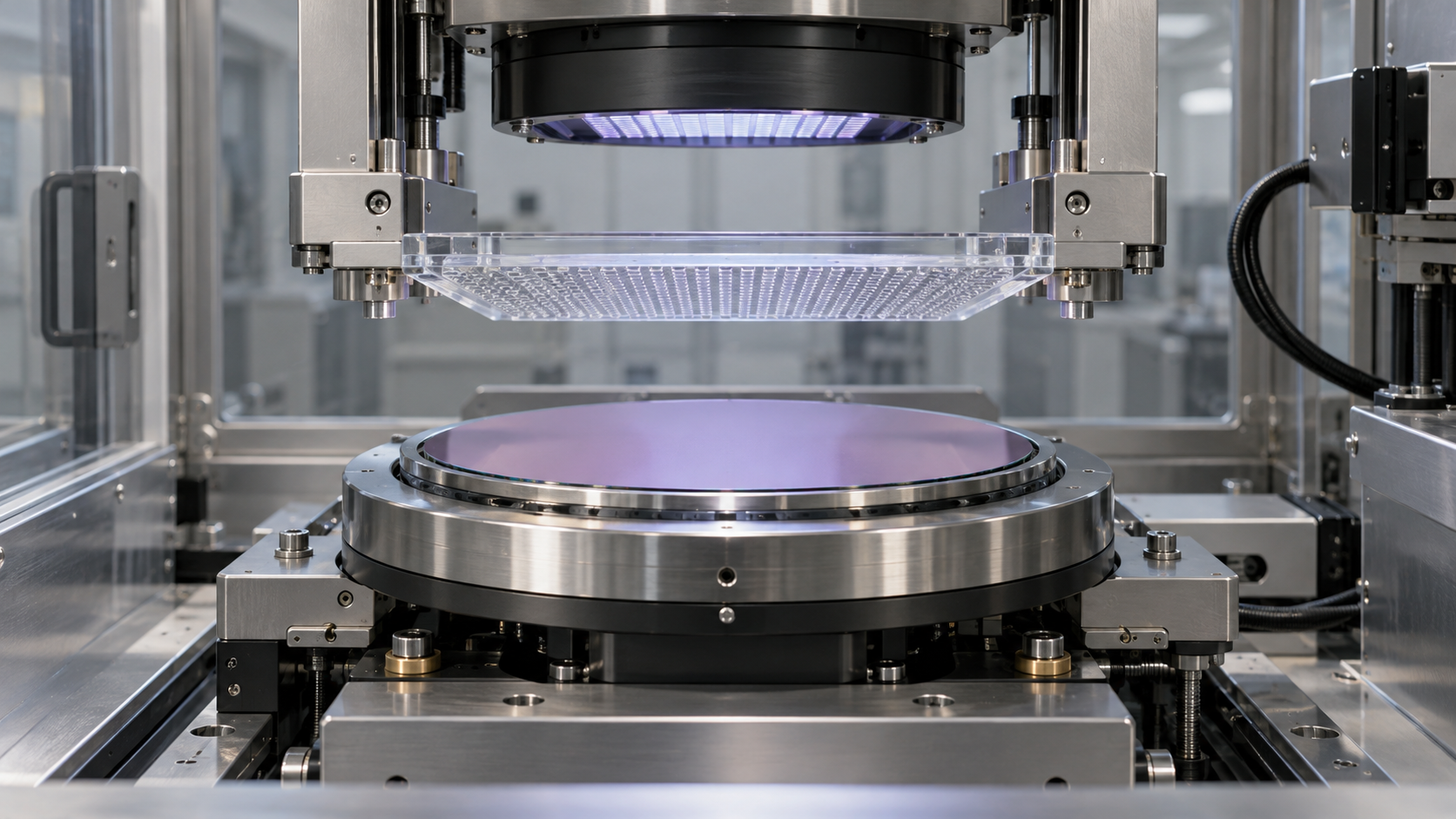
Nanoimprint lithography (NIL): a way to print without light, by pressing a mold carrying the circuit pattern into resin on the wafer
Canon is a Japanese company best known for cameras and office multifunction devices, but this profile covers only one part of its semiconductor equipment: nanoimprint lithography (NIL). In NIL, a mold carrying the circuit pattern (Canon calls it a "mask") is pressed into resin applied to the wafer, and the pattern is copied from it. Because the pattern transfer does not pass through an optical system, Canon says fine patterns on the mask can be reproduced faithfully. The company's stated values (at the 2023 launch) are a minimum linewidth of 14 nm (equivalent to the 5 nm node), with 10 nm (2 nm node equivalent) expected if mask technology improves (the latter is an expectation, not a result). Canon launched the FPA-1200NZ2C on 13 October 2023. In its July 2026 results briefing it said it had moved to a production-verification phase on customers' own wafers, aimed at volume use in 2027. Sales, shipment counts and customer names for NIL alone are not disclosed. This profile takes a nanofabrication view (mold accuracy, resin dispensing, alignment, particles), and sets out what primary sources confirm and what they do not.
- Canon in 30 seconds, and where it stands in nanotechnology
- The logo and how the name is written
- Where the company sits in the nanotechnology field
- Scale
- Resources committed to nanotechnology
- What it has done so far
- What comes next
- What the company is aiming for in nanotechnology
- Map of partnerships in nanotechnology
- Technologies, products and services
- The risks this company carries
- Glossary, references and claim-to-source audit
1. Canon in 30 seconds, and where it stands in nanotechnology
Unlike EUV, NIL is a method whose success depends not on the wavelength of light but on mold accuracy, alignment of mold and substrate, and control of foreign particles Our calculation. Canon's technology page says that because the mold is pressed directly into the resin on the wafer, the hard parts are aligning transferred patterns tens of nanometers in size with the layer below to nanometer accuracy, and managing particles caught between mold and wafer Sourced. The tool was launched in 2023, shipped to a Texas consortium in 2024, and in June 2026 shipped again to customers that are evaluating it. But whether NIL has begun to be used on a volume production line cannot be confirmed from the documents reviewed Not yet confirmed.
2. The logo and how the name is written

A note on names: the company is Canon Inc. (Kabushiki Kaisha; written "Canon" in English). Its U.S. nanoimprint subsidiary is Canon Nanotechnologies, Inc., renamed in 2014 from Molecular Imprints, Inc. of Austin, Texas. The logo was made from the shapes in the company's official website logo SVG; only the "Canon" shapes were taken and saved as a standalone SVG (the word "Global" in the original was left out).
Official website: https://global.canon/3. Where the company sits in the nanotechnology field
4. Scale
Canon is a large company, so this profile gives company-wide figures briefly and concentrates on the Industrial business unit (semiconductor lithography and related equipment) that bears on nanofabrication. The fiscal year is the calendar year and amounts are in yen (U.S. GAAP). Canon notified the SEC in March 2024 that its U.S. reporting obligations had ended (Form 15F), so this profile uses Canon's own investor-relations documents as primary sources.
| Measure (¥100 million) | 2025 | 2024 |
|---|---|---|
| Net sales (company-wide) | 46,247 | 45,098 |
| Operating profit (company-wide) | 4,554 | 4,449 (excluding the impairment loss) |
| Net income (company-wide) | 3,321 | 3,251 (same basis) |
| R&D expenses (company-wide) | 3,393 | 3,373 |
| Capital expenditure (company-wide) | 2,622 | 2,370 |
| Industrial business unit sales | 3,611 | 3,517 |
| of which Optical equipment (semiconductor and FPD lithography, etc.) | 2,564 | 2,534 |
| Industrial business unit operating profit | 625 | 689 |
| Employees (Industrial unit / company-wide) | 7,757 / 165,547 (our sum) | n/a |
The company-wide headcount is our sum of the headcounts of the five business units in the Annual Report (105,938, 13,347, 26,367, 7,757 and 12,138).
Semiconductor lithography unit sales were 234 units in 2025, with a plan of 227 units for 2026 (as of July 2026: 70 KrF and 157 i-line; the company's outlook) Sourced. Nanoimprint units are not shown separately in this breakdown (it has only the KrF and i-line categories). In the first half of 2026 the Industrial unit had sales of ¥145.2 billion (-9.1% year on year) and operating profit of ¥17.4 billion. The outlook for full-year 2026 is sales of ¥353.7 billion (-2.1%) and operating profit of ¥60.3 billion (as of 27 July 2026) Not yet confirmed.
Sales, profit and shipment counts for nanoimprint equipment are not given as separate figures in the documents reviewed. The results briefings describe shipments and progress in words only (for example, "additional systems were shipped in June 2026") without counts or amounts. We do not estimate the NIL portion Not yet confirmed.
5. Resources committed to nanotechnology
| Resource | What primary sources confirm | Status |
|---|---|---|
| People | The Industrial unit has 7,757 employees (2025). Canon's U.S. nanoimprint work is carried out together with its subsidiary Canon Nanotechnologies, and the technology page says the alignment measurement technology was developed in that collaboration. Headcount for NIL alone is not disclosed | Sourced / partly undisclosed |
| Money (R&D and capital expenditure) | Company-wide R&D was ¥339.3 billion (2025, 7.3% of sales) and capital expenditure ¥262.2 billion. The NIL share is not disclosed. In October 2022 Canon announced a new manufacturing building at its Utsunomiya Office (construction cost about ¥38 billion, operation planned for the first half of 2025; scope: R&D, manufacture and services for semiconductor lithography, with no NIL-specific capacity given). Actual start of operation could not be confirmed in Canon's own materials | Sourced / partly undisclosed |
| Acquisitions, investments, joint ventures, divestments | Molecular Imprints, Inc. (Austin, Texas) became a wholly owned subsidiary on 18 April 2014 and was renamed Canon Nanotechnologies, Inc. Canon says it began nanoimprint research in 2004 and, from 2009, ran joint development with MII and a major semiconductor manufacturer. The purchase price could not be confirmed in the documents reviewed | Sourced / price not confirmed |
| Universities, research institutes, public funding | A system was shipped to the Texas Institute for Electronics (TIE) (announced 26 September 2024). TIE is a semiconductor consortium supported by The University of Texas at Austin, made up of state and local governments, companies and national research institutions, and the system is for R&D and prototyping. The technology page says the NIL work of Canon, Dai Nippon Printing and KIOXIA received an Award of Excellence at the 49th Environmental Awards (2022), which the Ministry of the Environment supported. Specific public funding names and amounts could not be confirmed | Sourced / grant details not confirmed |
Status of key products and facilities
| Product / facility | Content (company's stated values) | Stage | Date / source |
|---|---|---|---|
| FPA-1200NZ2C (NIL semiconductor manufacturing system) | Minimum linewidth 14 nm (5 nm node equivalent). Overlay accuracy of 4 nm or better. 300 mm wafers, 6-inch mask, 26 × 33 mm field | Launched (13 October 2023) | 13 October 2023 (References 5, 6) |
| System delivered to TIE | For R&D and prototyping. TIE is a semiconductor consortium supported by The University of Texas at Austin | Shipped (announced 26 September 2024) | 26 September 2024 (Reference 7) |
| Shipments to a major semiconductor manufacturer (name not disclosed) | In January 2026 Canon said the customer had confirmed the specifications of the shipped system. Another system was shipped in June 2026 to a customer that is evaluating it | Under evaluation and verification (use on a volume line could not be confirmed) | January and July 2026 (References 2, 3, 4) |
| IAP (inkjet-based adaptive planarization) | Adapts NIL technology to planarization. Canon says surface irregularity is reduced to 5 nm or less. It aims to commercialize equipment in 2027 | Developed; commercialization is a plan (Not yet confirmed) | 13 January 2026 (Reference 8) |
| Volume use of NIL | A production-verification phase using customers' wafers, assuming actual manufacturing lines, aimed at volume use in 2027. Several customers are verifying for volume production | Not yet confirmed (company statement) | 27 July 2026 (Reference 3) |
6. What it has done so far
| When | What happened | Why it matters |
|---|---|---|
| 2004 | Canon began research on nanoimprint, aiming at high-resolution processes below 20 nm | A search for a method that does not use light |
| 2009 | Joint development began with Molecular Imprints and a major semiconductor manufacturer (Canon's statement). DNP also says it began joint development of NIL processes with Toshiba and Canon in 2009 | Tool, mold and chip-process makers working together |
| 2014 | Agreement to make MII a wholly owned subsidiary in February, completed on 18 April. Renamed Canon Nanotechnologies | Brings in U.S. NIL technology and patents |
| 23 February 2017 | DNP announced it would introduce equipment for making NIL replica templates (copies of the mold) from March of that year and begin supplying 10 nm-scale templates | Setting up volume production of molds |
| 2022 | The NIL work of Canon, DNP and KIOXIA received an Award of Excellence at the Environmental Awards (for lower power use). In October Canon announced a new building at Utsunomiya | Recognition for power savings; preparing production capacity |
| 13 October 2023 | Launched the NIL semiconductor manufacturing system FPA-1200NZ2C. Canon says it is the world's first commercialization of semiconductor equipment using NIL | Entry to the market as a product |
| 8 March 2024 | At its strategy conference Canon compared NIL with EUV when forming a 15 nm pattern (Canon's estimate): power use 0.13 (-87% against EUV at 1.00) and cost per wafer 0.77 (-23%) | The basis of the low-power, low-cost pitch (a company estimate) |
| 26 September 2024 | Shipment of the FPA-1200NZ2C to TIE announced | Introduction at a U.S. research site |
| 9 December 2025 | DNP announced an NIL template with a 10 nm line pattern (equivalent to the 1.4 nm generation of logic). It has begun evaluation with customers and aims to start volume production in 2027 | Finer molds |
| 13 January 2026 | Announced practical implementation, a world first by its own account, of planarization (IAP) based on nanoimprint technology | NIL know-how reaches other steps |
| 27 July 2026 | Shipped another system in June to a customer that is evaluating it. Said it had moved to production verification on customers' wafers, aimed at volume use in 2027 | From evaluation to production verification |
7. What comes next
The primary sources also contain the following policies and plans Not yet confirmed.
- Challenges toward volume production: in a Canon engineer interview, the next goals are extending mask (mold) life and lowering cost so that customers can run the tool as easily as conventional equipment. Particle control and the accuracy of transfer at the wafer edge (partial fields) are also named as challenges
- Widening applications: at the 2023 launch Canon cited "metalenses for XR with microstructures of tens of nanometers" and other optical elements. Materials from its September 2024 business strategy conference show logic (wiring layers), DRAM, 3D NAND and optical elements (such as metalenses) as applications
- Supply of molds: Dai Nippon Printing (DNP) aims to start volume production of NIL templates in 2027, with a target of ¥4 billion in NIL sales in fiscal 2030 (DNP's plan)
- 2026 plan for semiconductor lithography: 227 units in total (70 KrF and 157 i-line). NIL units are not shown
Sales, profit, shipment counts, production capacity and R&D for NIL / the names of customers that have decided to adopt it for volume production / the name of the "major semiconductor manufacturer" / the actual start of operation of the new Utsunomiya building (in Canon's own materials) / the purchase price of Molecular Imprints / specific public funding names and amounts. Either the documents reviewed (the results materials, news releases, technology pages and DNP releases) do not state them, or we could not check the original text.
8. What the company is aiming for in nanotechnology
This section separates what the company says it aims for from what we read into it. Inference marks our interpretation of primary sources.
| What can be read | Primary basis | Type |
|---|---|---|
| Sell NIL as low-power, low-cost fine patterning | The 2023 launch release says no light source with a special wavelength is needed, so power use falls significantly. The technology page says complex 2D and 3D patterns form in a single pass and power use could be about one tenth of advanced logic exposure (the basis of comparison is not stated). The strategy conference gives Canon's estimates against EUV for a 15 nm pattern: power use -87% and cost per wafer -23% | Sourced (company description and estimate) |
| Begin volume use in specific steps such as memory (3D NAND, DRAM) | It shows microscope images of 3D NAND hole and dual damascene steps and DRAM hole and cut steps as applications (sources: KIOXIA, Canon). Its 2024 strategy is to promote use in volume processes, particularly with major semiconductor manufacturers | Sourced (description) / Inference (which use comes first) |
| Extend NIL know-how to other steps such as planarization | It announced IAP in January 2026 and aims to commercialize it in 2027. The interview says IAP started from a customer-site problem: misalignment caused by surface irregularity on the wafer | Sourced |
| Build it up with partners in molds and chip processes | The cooperation of DNP (molds), KIOXIA (chip manufacturing technology) and Canon (tools) was recognized by the Environmental Awards. DNP has co-developed since 2009 | Sourced (description of the cooperation) / Inference (whether it continues this way) |
The reading that "for now NIL will enter volume use from specific steps such as memory" rests on the materials of the March 2024 strategy conference. They show cross-sections of specific steps in NAND and DRAM, such as "hole" and "cut", with sources given (KIOXIA, Canon), and for logic only an example of the wiring layers (BEOL; the source is The University of Texas) Sourced. The company also names "3D single patterning" (making a complex 3D pattern in one imprint) as a strength Sourced. From this we read that NIL is likely to be used first not by replacing every layer, but in steps where being able to make the pattern in one shot gives the greatest benefit. However, Canon's documents do not say which customer has decided to adopt NIL for which step Not yet confirmed.
9. Map of partnerships in nanotechnology
The main NIL partnerships that the documents reviewed confirm are DNP (manufacture of molds, and joint development since 2009), KIOXIA (the chip-manufacturing side; the three companies shared an environmental award), Canon Nanotechnologies (a U.S. subsidiary that co-developed alignment technology and more) and TIE (a recipient of a system) Sourced. The shipment to a "major semiconductor manufacturer" is mentioned in Canon's results briefings, but no name is given. The supplier of resin (resist) for NIL, and any individual contracts Canon has with resin makers, are not in the documents reviewed Not yet confirmed.
10. Technologies, products and services
This profile covers nanoimprint equipment and related technology (Canon's other lithography tools and products are out of scope). Performance numbers are the company's own statements, and conditions are given with them.
| Category | What official material says | Conditions, scale, source |
|---|---|---|
| NIL semiconductor manufacturing system (FPA-1200NZ2C) | Presses a mask carrying the circuit pattern into the resist on the wafer "like a stamp". Because the transfer does not pass through an optical system, fine mask patterns are reproduced faithfully. Complex 2D and 3D patterns can be formed in a single imprint, which may lower the cost of ownership (CoO) | Company statement (product page, 2023). Minimum linewidth 14 nm (5 nm node equivalent). Conditions such as throughput are not given |
| Main specifications | Field 26 × 33 mm, 6-inch mask, 300 mm (12-inch) wafer, overlay accuracy 4 nm or better, body (W) 2,700 × (D) 6,600 × (H) 2,830 mm (2 stations) | Manufacturer's stated value (product page). The measurement conditions for overlay accuracy are not given |
| Alignment and particle control | Mask-to-wafer misalignment is measured in real time with moiré patterns at nanometer accuracy. Alignment to lower layers uses laser heating to deform the wafer (a DMD varies the heating pattern). Environment control inside the tool (high-performance filters, air curtains and others) holds down particles | Company statement (technology page). Quantitative performance values are not given |
| Estimate of power use and cost | For a 15 nm pattern, with EUV at 1.00, NIL power use is 0.13 and cost per wafer is 0.77 | Canon's estimate (strategy conference materials, 8 March 2024). The conditions of the EUV tool and process compared are not given |
| IAP (inkjet-based adaptive planarization) | An inkjet dispenses light-curable material to match the wafer's surface topography, and a flat glass plate is pressed on. A whole 300 mm wafer is planarized in one stamp, and irregularity is reduced to 5 nm or less | Company statement (13 January 2026). It aims to commercialize in 2027 (Not yet confirmed). The comparison with spin coating and CMP is Canon's own |
According to Canon's technology page, NIL started from controlling the amount and position of resin. So that the resin is not squeezed out when the mask is pressed in, and so that a resin layer of uniform thickness forms whatever the size or number of the mask's indentations, Canon developed technology that decides precisely how much resin the inkjet places and where Sourced. The IAP release likewise describes NIL as applying resist to the wafer with an inkjet and then pressing a patterned mask on "like a stamp", and says IAP dispenses light-curable material to match surface topography Sourced. Next, so that the convex fine patterns formed in the resin do not deform when the mask is pulled away cleanly, Canon says it developed nanometer-level control technology Sourced. The resin's composition (viscosity, curing mechanism, shrinkage, ease of release), the mold material and its surface treatment are not in the documents reviewed. Also, because the mold actually contacts the wafer, mold life is a challenge: the engineer interview says extending mask life and cutting cost are the next goals Sourced. On the mold-making side, DNP announced a template with a 10 nm line pattern (December 2025) Sourced. Note that the comparison with EUV (power use -87% and so on) is Canon's estimate for a 15 nm pattern, and does not rank NIL against other methods.
11. The risks this company carries
| Risk | What it involves | Type |
|---|---|---|
| The scale of the NIL business is hard to see from outside | Sales, shipment counts, customer names and capacity are not disclosed, so statements that adoption for volume use is advancing cannot be checked against figures | Sourced |
| Verification for volume use is still under way | Even in July 2026 the stage is production verification on customers' wafers. Volume adoption is a 2027 target, and we could not confirm any decision to adopt | Not yet confirmed |
| Mold (mask) life and cost | Because the mold touches the wafer directly, Canon's engineer says extending its life and cutting its cost are the next challenges. Mold manufacturing also depends on outside makers such as DNP | Sourced (company statement) |
| Particles and overlay | The technology page says that if a particle is caught between mold and wafer, it can cause not only defective devices but destruction of the pattern on the mask itself. Overlay accuracy and transfer accuracy at the wafer edge are also named as challenges | Sourced (company statement) |
| Dependence on semiconductor investment | In the first half of 2026 the Industrial unit's sales fell 9.1% year on year (the fall in display manufacturing equipment was large). Semiconductor lithography was led by equipment for memory and for AI-related back-end processes. I-line sales are expected to fall in 2026 | Sourced |
| Progress in competing methods | On the EUV side, tools with a higher numerical aperture have also shipped (ASML's announcements; see our ASML profile). Which method is adopted for which use is up to the customer. This profile does not rank them | Sourced (another company's announcement) / Inference (future competition) |
| Burden of people and investment | Company-wide R&D was ¥339.3 billion and capital expenditure ¥262.2 billion in 2025, and the 2026 capital expenditure plan is ¥270.0 billion. The allocation to NIL is not disclosed | Sourced |
12. Glossary
- Nanoimprint lithography (NIL)
- A method that presses a mold into resin on the wafer to copy a nanoscale pattern. See our explainer on self-assembly and nanoimprint.
- Mask (template)
- The mold carrying the circuit pattern. Canon calls it a "mask" and DNP a "template".
- Resist (resin)
- The resin applied to the wafer. In NIL it is shaped by the mold and then cured with light. See our explainer on resists and photomasks.
- Inkjet dispensing
- Placing resin as tiny droplets, in the amount needed and only where needed.
- Overlay accuracy
- How far the pattern being printed is off from the pattern of the layer below.
- Particle
- A foreign particle. In NIL one caught between mold and wafer can cause defects or damage the mold.
- nm node
- A name for a generation of semiconductor technology. It does not equal the linewidth itself (Canon's note).
- Planarization
- The step that removes surface irregularity from a wafer. IAP does it with an inkjet and a glass plate.
- 3D single patterning
- Forming a complex three-dimensional pattern in one imprint (Canon's term).
- Cost of ownership (CoO)
- A way of counting the total cost per wafer, including purchase, operation and maintenance of the tool.
13. References
- Canon Consolidated Financial Results for the Fiscal Year Ended December 31, 2025 (29 January 2026). Company-wide sales, profit and R&D, and the Industrial business unit. https://global.canon/en/ir/results/2025/rslt2025e.pdf
- Canon FY 2025 Results presentation (29 January 2026). Industrial Group sales and operating profit, semiconductor lithography unit sales, and progress on nanoimprint. https://global.canon/en/ir/conference/pdf/conf2025e-note.pdf
- Canon Second Quarter 2026 Results presentation (27 July 2026; in Japanese). 2026 outlook for the Industrial Group, lithography unit sales, and progress on production verification of nanoimprint. https://global.canon/ja/ir/conference/pdf/conf2026q2j-note.pdf
- Canon Canon Annual Report 2025. Sales and headcount by business unit, and the Industrial Group strategy. https://global.canon/en/ir/annual/canon-annual-report-2025-03.pdf
- Canon News release "Nanoimprint lithography semiconductor manufacturing system that covers diverse applications with simple patterning mechanism" (13 October 2023). Launch of the FPA-1200NZ2C. https://global.canon/en/news/2023/20231013.html
- Canon Product page "FPA-1200NZ2C". Features and specifications (field size, mask, wafer, overlay accuracy). https://global.canon/en/product/indtech/semicon/fpa1200nz2c.html
- Canon News release "Canon delivers FPA-1200NZ2C nanoimprint lithography system for semiconductor manufacturing to the Texas Institute for Electronics" (26 September 2024). https://global.canon/en/news/2024/20240926.html
- Canon News release "Canon achieves world first with novel inkjet-based wafer planarization, delivering dramatically smoother wafer surfaces" (13 January 2026). https://global.canon/en/news/2026/20260113-2.html
- Canon Technology page "Nanoimprint Lithography". The NIL principle, alignment, particle control and the award. https://global.canon/en/technology/canon-tech/tech/nil/
- Canon Engineer interview "Optimizing Mass Production Lines in Semiconductor Manufacturing". Optimizing mass production lines and remaining challenges. https://global.canon/en/technology/canon-tech/interview/nanoimprint/
- Canon News release "Canon to make Molecular Imprints a wholly owned subsidiary" (14 February 2014). Background of nanoimprint research and the agreement to acquire. https://global.canon/en/news/2014/feb14e.html
- Canon News release "Canon completes acquisition of Molecular Imprints" (23 April 2014). The renaming to Canon Nanotechnologies, Inc. https://global.canon/en/news/2014/apr23e02.html
- Canon News release "Canon Utsunomiya Office to install new manufacturing facilities, strengthen manufacturing capacity for semiconductor lithography systems" (6 October 2022). https://global.canon/en/news/2022/20221006-2.html
- Canon 2024 Corporate Strategy Conference, Industrial Group (8 March 2024). Applications of nanoimprint and the comparison with EUV on power use and cost per wafer (Canon's estimate). https://global.canon/en/ir/conference/pdf/housin2024ind-e.pdf
- Canon Industrial Group Business Strategy Conference (10 September 2024). Nanoimprint applications and production sites. https://global.canon/en/ir/conference/pdf/event2024ind-e.pdf
- Dai Nippon Printing (DNP) News release "DNP to Introduce Nanoimprint Replica Template Manufacturing Equipment and Establish Volume Production System for 10nm-Scale Semiconductors" (23 February 2017). Joint development with Toshiba and Canon since 2009. https://www.global.dnp/en/news/detail/2017/02/0223_20166784/
- Dai Nippon Printing (DNP) News release "DNP Achieves 10nm Line-pattern resolution on Nanoimprint Template for Cutting-Edge Semiconductors" (9 December 2025). https://www.global.dnp/en/news/detail/2025/12/1209_20177718/
- Canon Company website (source of the logo; only the "Canon" shapes were taken from the site's logo SVG and saved as a standalone SVG). https://global.canon/01cmn/img/common/logo.svg
- U.S. SEC Canon Inc. Form 15F (filed 7 March 2024; notice ending its U.S. reporting obligations). EDGAR filing. https://www.sec.gov/Archives/edgar/data/16988/000119312524061282/d810759d15f12b.htm

14. Claim-to-source audit
| Claim in the text | Type | Source |
|---|---|---|
| Canon Inc. is headquartered in Shimomaruko, Ohta-ku, Tokyo, and listed on the Tokyo Stock Exchange and others (code 7751), under U.S. GAAP. On 7 March 2024 it filed Form 15F ending its U.S. reporting obligations | Sourced | Reference 1 https://global.canon/en/ir/results/2025/rslt2025e.pdf Reference 19 https://www.sec.gov/Archives/edgar/data/16988/000119312524061282/d810759d15f12b.htm |
| 2025 company-wide: net sales of ¥4,624.7 billion (2024: ¥4,509.8 billion), operating profit of ¥455.4 billion (2024: ¥444.9 billion excluding the impairment loss), net income of ¥332.1 billion, R&D expenses of ¥339.29 billion (7.3% of sales), capital expenditure of ¥262.2 billion | Sourced | Reference 1 https://global.canon/en/ir/results/2025/rslt2025e.pdf Reference 2 https://global.canon/en/ir/conference/pdf/conf2025e-note.pdf |
| Industrial business unit: 2025 sales of ¥361.1 billion (+2.7%), operating profit of ¥62.5 billion, optical equipment ¥256.4 billion, industrial equipment ¥104.7 billion. 2024: sales ¥351.7 billion, operating profit ¥68.9 billion | Sourced | Reference 1 https://global.canon/en/ir/results/2025/rslt2025e.pdf Reference 2 https://global.canon/en/ir/conference/pdf/conf2025e-note.pdf |
| Employees: 7,757 in the Industrial unit; company-wide total of 165,547 (105,938 + 13,347 + 26,367 + 7,757 + 12,138) | Our calculation | Our calculation. Headcounts by unit are in Reference 4. Reference 4 https://global.canon/en/ir/annual/canon-annual-report-2025-03.pdf |
| Semiconductor lithography unit sales: 234 in 2025 and a plan of 227 for 2026 (70 KrF, 157 i-line). NIL units are not shown in the breakdown | Sourced | Reference 2 https://global.canon/en/ir/conference/pdf/conf2025e-note.pdf Reference 3 https://global.canon/ja/ir/conference/pdf/conf2026q2j-note.pdf |
| First half of 2026, Industrial unit: sales of ¥145.2 billion (-9.1% year on year), operating profit of ¥17.4 billion. 2026 outlook: sales of ¥353.7 billion (-2.1%), operating profit of ¥60.3 billion (as of 27 July 2026) | Not yet confirmed | The company's outlook (full year); the first half is actual. Reference 3 https://global.canon/ja/ir/conference/pdf/conf2026q2j-note.pdf |
| The FPA-1200NZ2C was launched on 13 October 2023, Canon's statement is that it is the world's first commercialization of NIL semiconductor equipment. Minimum linewidth 14 nm (5 nm node equivalent); 10 nm (2 nm node equivalent) expected with better mask technology | Sourced | Company statement. 10 nm is an expectation, not a result. Reference 5 https://global.canon/en/news/2023/20231013.html Reference 6 https://global.canon/en/product/indtech/semicon/fpa1200nz2c.html |
| Specifications: field 26 × 33 mm, 6-inch mask, 300 mm wafer, overlay accuracy 4 nm or better, body 2,700 × 6,600 × 2,830 mm (2 stations) | Sourced | Manufacturer's stated value. Reference 6 https://global.canon/en/product/indtech/semicon/fpa1200nz2c.html |
| On 26 September 2024 Canon announced it would ship an FPA-1200NZ2C to the Texas Institute for Electronics (TIE), founded in 2021 and supported by The University of Texas at Austin, for R&D and prototyping | Sourced | Reference 7 https://global.canon/en/news/2024/20240926.html |
| January 2026: the specifications of the system shipped to a major semiconductor manufacturer were confirmed by the customer. 27 July 2026: a further system shipped in June to a customer under evaluation; production verification on customers' wafers aimed at volume use in 2027; several customers verifying; more shipments planned | Not yet confirmed | Company statement. Adoption in volume production could not be confirmed. Reference 2 https://global.canon/en/ir/conference/pdf/conf2025e-note.pdf Reference 3 https://global.canon/ja/ir/conference/pdf/conf2026q2j-note.pdf Reference 4 https://global.canon/en/ir/annual/canon-annual-report-2025-03.pdf |
| IAP: an inkjet dispenses light-curable material and a flat glass plate is pressed on, reducing irregularity to 5 nm or less, across a whole 300 mm wafer in one stamp. Commercialization aimed at 2027 | Not yet confirmed | Company statement and plan. Reference 8 https://global.canon/en/news/2026/20260113-2.html |
| The NIL principle and challenges: control of resin amount and position, no deformation of the pattern on release, nanometer-level alignment (moiré, laser-induced thermal deformation) and particle control. Power use could be about one tenth of advanced logic exposure (basis of comparison not stated) | Sourced | Company statement. Reference 9 https://global.canon/en/technology/canon-tech/tech/nil/ |
| Challenges toward volume production: extending mask life and lowering cost, transfer at the wafer edge, and operation as easy as conventional equipment | Sourced | An engineer's remarks (company statement). Reference 10 https://global.canon/en/technology/canon-tech/interview/nanoimprint/ |
| MII became a wholly owned subsidiary on 18 April 2014 and was renamed Canon Nanotechnologies, Inc. Research began in 2004 and joint development in 2009 | Sourced | Reference 11 https://global.canon/en/news/2014/feb14e.html Reference 12 https://global.canon/en/news/2014/apr23e02.html |
| A new building at Utsunomiya is planned: area of about 70,000 m², construction cost of about ¥38 billion, construction starting in the second half of 2023, operation in the first half of 2025 (announced 6 October 2022; scope is R&D, manufacture and services for semiconductor lithography) | Not yet confirmed | A plan; actual operation could not be confirmed in Canon's own materials. Reference 13 https://global.canon/en/news/2022/20221006-2.html |
| Strategy conference (8 March 2024): for a 15 nm pattern, NIL power use is 0.13 (-87%) and cost per wafer 0.77 (-23%) against EUV at 1.00. Applications: NAND, DRAM, logic, optical elements | Sourced | Canon's estimate ("Canon est."). Reference 14 https://global.canon/en/ir/conference/pdf/housin2024ind-e.pdf |
| 10 September 2024 conference: NIL applications and production at the Utsunomiya Optical Products Operations | Sourced | Reference 15 https://global.canon/en/ir/conference/pdf/event2024ind-e.pdf |
| DNP: joint development of NIL processes with Toshiba and Canon since 2009; replica template manufacturing equipment introduced from March 2017 | Sourced | Reference 16 https://www.global.dnp/en/news/detail/2017/02/0223_20166784/ |
| DNP: on 9 December 2025 it developed an NIL template with a 10 nm line pattern (1.4 nm generation equivalent). It aims to start volume production in 2027 and ¥4 billion of NIL sales in fiscal 2030 | Not yet confirmed | DNP's plan. Reference 17 https://www.global.dnp/en/news/detail/2025/12/1209_20177718/ |
| The NIL work of Canon, DNP and KIOXIA received an Award of Excellence at the 49th Environmental Awards (2022) | Sourced | Reference 9 https://global.canon/en/technology/canon-tech/tech/nil/ |
| Sales, profit, shipment counts, capacity and R&D for NIL; names of customers that decided to adopt volume production; the name of the "major semiconductor manufacturer"; the purchase price of Molecular Imprints; specific public funding names and amounts | Not yet confirmed | Not stated in the documents reviewed, so not confirmed. We do not estimate them (outlook). |
| The logo is the "Canon" shapes taken from the site's logo SVG | Sourced | Reference 18 https://global.canon/01cmn/img/common/logo.svg |
| The four-type grouping and the example company names | Our calculation | Our own grouping. Company names are examples from companies covered in this series. |
| "NIL succeeds or fails on mold accuracy, alignment and particle control, not on the wavelength of light" | Our calculation | Our own synthesis, from the challenges described on the technology page and in the interview (References 9, 10). |
| The reading that NIL will enter volume use first in steps where a one-shot pattern gives the greatest benefit, such as memory | Inference | Our interpretation of how the strategy conference materials present applications. Reference 14 https://global.canon/en/ir/conference/pdf/housin2024ind-e.pdf Reference 15 https://global.canon/en/ir/conference/pdf/event2024ind-e.pdf |
| The reading that EUV and NIL may compete in some uses | Inference | This article's interpretation. Other companies' announcements are not detailed here (see our ASML profile). |
Last updated 9 October 2026 / Troy Technical
Figures in this article come from Canon's results releases and briefing materials, Annual Report, news releases, and product and technology pages, and from Dai Nippon Printing's releases. No research-firm estimates or press-based figures have been used. The tool's performance values (minimum linewidth, overlay accuracy) are the manufacturer's stated values, and the comparison with EUV is Canon's own estimate; neither ranks one method against another. The company's outlooks and plans are its own statements and have not been independently verified. Passages marked "Inference" are this article's interpretation of primary sources, not statements made by the company.