COMPANY PROFILE / NANOTECHNOLOGY
EV Group (EVG)
A privately held Austrian equipment maker whose tools press nanopatterns into resin and bond wafers together with nanometer-level alignment
EV Group (EVG) is an Austrian equipment maker known for nanoimprint lithography (NIL) and wafer bonding. It was founded in 1980 and says it has more than 1,700 employees. Nothing in its official material points to a stock market listing, and it does not publish financial results; this article treats it as privately held. The company says its SmartNIL process has production-proven resolution down to 40 nm and smaller (company statement). In May 2026, together with imec, it reported wafer-to-wafer hybrid bonding at a 200 nm interconnect pitch (a joint announcement by the company and the research institute). Revenue, sales by customer and the number of tools sold do not appear in the official material this article reviewed. This profile sets out, from the company's website and news releases, what it makes, where it invests, who it works with and which parts are results and which are plans.
- EV Group in 30 seconds, and where it stands in nanotechnology
- The logo and how the name is written
- Where the company sits in the field
- Scale (what is disclosed)
- Resources committed to nanotechnology
- What it has done so far
- What comes next
- What the company is aiming for in nanotechnology
- Map of partnerships in nanotechnology
- Technologies, products and services
- The risks this company carries
- Glossary, references and claim-to-source audit
1. EV Group in 30 seconds, and where it stands in nanotechnology
AustriaFounded in 1980 by Aya Maria and Erich Thallner, per the company
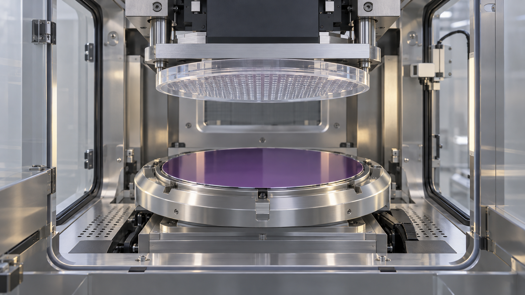
EVG's tools do not "write" patterns with an electron beam or extreme ultraviolet light. They either press a mold (stamp) into resin to copy a nanopattern (NIL), or stack wafers and bond them together (bonding). The company says the former is used for large-area nanostructures such as augmented-reality (AR) waveguides, metalenses (lenses built from nanostructures) and microfluidic chips, and the latter for 3D stacking of chips such as AI processors Sourced. The company calls itself the market-leading NIL equipment supplier, and in bonding claims "the leading position and dominant market share", but no figures support either statement. This article reports them as company claims, not as fact. Because EVG is privately held and publishes no financial figures, the "scale" section here is limited to headcount, facility area and sites that official material confirms.
2. The logo and how the name is written

A note on names: the company is EV Group (abbreviated EVG). Legal entity names differ by country and site; the official Imprint names EV Group Europe & Asia/Pacific GmbH as publisher. SmartNIL, HERCULES, BONDSCALE, LITHOSCALE and ComBond are product and technology names, not company names. The logo was taken from the header of the company's official website (the original is white, a version for dark backgrounds).
Official site: https://www.evgroup.com/3. Where the company sits in the field
EVG's main type is nanofabrication & equipment. The company itself lists "nanotechnology devices" among the products its equipment is used to make, and supplies equipment and processes for nanofabrication Sourced (see Reference 3 https://www.evgroup.com/company/rd-projects Reference 6 https://www.evgroup.com/products/nanoimprint-lithography). The table below arranges the processes and technologies that appear in its materials.
| Process / technology | Role in nanofabrication | Figures and uses given by the company (company statements) | Type |
|---|---|---|---|
| Nanoimprint (SmartNIL) | A soft stamp presses a nanopattern into UV-curable resin. A room-temperature process; the stamp is reused | Production-proven resolution of 40 nm and below. Wafers up to 300 mm, and panels. Uses: AR waveguides, diffractive optical elements, metalenses, microfluidic chips, wire-grid polarizers | Sourced (company statement) |
| Step-and-repeat (master fabrication for NIL) | A small master mold is stamped repeatedly to build a large-area master | The EVG770 NT scales to 300 mm wafers and Gen-2 panels. A contract mastering service (S&R Mastering Shop) is also offered | Sourced |
| Hybrid and fusion bonding | Bonds the dielectric layers and copper pads of two wafers, connecting them mechanically and electrically. A core step in 3D stacking | Alignment better than 100 nm (company description). Connection pitch below 1 µm. In May 2026, with imec, a 200 nm pitch, and post-bond overlay below 40 nm for all dies across a full 300 mm wafer | Sourced (joint release by the company and imec) |
| IR LayerRelease | An infrared laser releases an ultra-thin layer from a silicon carrier with nanometer precision | Removes the need for glass carriers in advanced packaging, and the company says it can transfer thin layers for next-generation transistor structures such as CFET | Sourced (company statement) |
| Lithography and metrology (secondary) | Maskless exposure (LITHOSCALE), resist processing, and bonding overlay metrology (EVG40 D2W) | LITHOSCALE XT: up to 5x the throughput of the previous model (company claim). EVG40 D2W measures the shift of every die on a 300 mm wafer | Sourced (company statement) |
All figures in the table are manufacturer's stated values, and the pages do not give measurement methods, samples or conditions. NIL resolution and bonding overlay are numbers for different technologies and should not be ranked against each other. Reference: Reference 5 https://www.evgroup.com/technologies/nanoimprint-lithography-smartnil Reference 7 https://www.evgroup.com/technologies/fusion-and-hybrid-bonding Reference 23 https://www.evgroup.com/company/news/detail/ev-group-unlocks-agile-and-efficient-production-scaling-with-next-generation-step-and-repeat-nanoimprint-lithography-system Reference 24 https://www.evgroup.com/company/news/detail/ev-group-launches-first-of-its-kind-step-and-repeat-mastering-services-for-nanoimprint-lithography Reference 10 https://www.evgroup.com/company/news/detail/imec-and-ev-group-demonstrate-wafer-to-wafer-hybrid-bonding-with-200nm-interconnect-pitch-and-record-high-overlay-accuracy Reference 9 https://www.evgroup.com/technologies/ir-layerrelease-technology Reference 34 https://www.evgroup.com/company/news/detail/ev-group-brings-digital-lithography-to-heterogeneous-integration-hvm-applications-with-lithoscaler-xt Reference 33 https://www.evgroup.com/company/news/detail/ev-group-achieves-breakthrough-in-hybrid-bonding-overlay-control-for-chiplet-integration
4. Scale (what is disclosed)
EVG's revenue, profit, total assets and order backlog are not published in the official material this article reviewed Not yet confirmed. The table is therefore limited to indicators that official sources confirm: headcount, facilities and sites.
| Indicator | Value | Note |
|---|---|---|
| Founded | 1980 | By Aya Maria and Erich Thallner, per the company |
| Employees | More than 1,700 | Worldwide; no reference date. In October 2024 the company said it planned to hire well over 100 people in the financial year then under way |
| Financial year | Starts on 1 October | The 24 October 2024 release says the "current financial year began on October 1, 2024" |
| Production area at headquarters | More than 8,100 m² | The Manufacturing V building, completed in November 2023, added more than 1,200 m² of production floor (total over 8,100 m²) and more than 1,200 m² of warehouse space |
| Test rooms at headquarters | About 2,800 m² | An existing building was converted at the same time, adding nine test rooms and raising test room area by 30% (also used by customers for acceptance inspection of equipment) |
| Cleanrooms | About 620 m² added by Cleanroom V | Completed in July 2020; the company said it nearly doubled the cleanroom capacity at headquarters. The investment was €30 million (announced in 2019) |
| Sites | Wholly owned subsidiaries in the U.S., Japan, South Korea, China, Taiwan and Singapore | U.S. sites in Arizona, New Mexico and Oregon; Japan in Yokohama and Fukuoka. Also Germany (Neuhaus), Malaysia (Penang; joint venture), and sales representatives in places such as Israel and Beijing |
| Certifications | ISO 9001 (first certified in 2004); environmental management system under ISO 14001 | Company statement |
Reference: Reference 1 https://www.evgroup.com/company/about-evg Reference 2 https://www.evgroup.com/company/global-presence Reference 16 https://www.evgroup.com/company/news/detail/ev-group-announces-management-board-expansion-in-light-of-unabated-growth Reference 15 https://www.evgroup.com/company/news/detail/ev-group-completes-construction-of-new-manufacturing-v-building-at-corporate-headquarters-to-expand-production-capacity Reference 18 https://www.evgroup.com/company/news/detail/ev-group-completes-construction-of-state-of-the-art-cleanroom-facility-at-corporate-headquarters-1595234788 Reference 17 https://www.evgroup.com/company/news/detail/ev-group-invests-30-million-euros-for-capacity-expansion-at-corporate-headquarters-in-austria-1561360823 Reference 31 https://www.evgroup.com/company/news/detail/ev-group-forms-subsidiary-in-singapore-to-strengthen-local-customer-support Reference 30 https://www.evgroup.com/company/news/detail/ev-group-and-dymek-company-form-joint-venture-company-in-malaysia-to-enhance-regional-customer-support
Expressions such as "market-leading" and "dominant share" are the company's own assessments, with no third-party statistics attached. The materials say EVG holds "the leading position and dominant market share" in wafer bonding and is "market-leading" in NIL, but give no share figures Not yet confirmed. The reference date of the headcount, R&D spending and order backlog could not be confirmed either.
5. Resources committed to nanotechnology
Headcount and R&D spending devoted to nanofabrication alone are not disclosed. The table covers what company-wide official material confirms.
| Resource | What primary sources confirm | Type |
|---|---|---|
| People | More than 1,700 employees. The company planned to hire well over 100 people worldwide in the financial year starting October 2024 (October 2024 release). R&D headcount is not disclosed. The management board includes the founders Erich Thallner and Aya Maria Thallner, Werner Thallner, Paul Lindner, Hermann Waltl, and Alexander Rank (joined in October 2024) | Sourced / partly undisclosed |
| Money (R&D) | R&D spending is not disclosed. EVG takes part in publicly supported joint research projects (see the last row) | Not found |
| Money (capex) | Continuing expansion of the headquarters: €30 million announced in 2019 for the Cleanroom V building (completed July 2020); the Manufacturing III building (1,800 m² of production floor) in 2019; Manufacturing V in November 2023; and Manufacturing VI, completed by October 2024. The amounts for V and VI are not disclosed | Sourced / partly undisclosed |
| Equity stakes, acquisitions, joint ventures, divestments | In May 2023, a joint venture with Dymek Company in Malaysia (EV Group Malaysia Dymek, which handles customer support). In May 2025, a wholly owned subsidiary in Singapore. In 2018, an agreement to license IBM's patented laser release technology. No large acquisition or divestment was found in the material reviewed | Sourced / not found |
| Universities, research institutes and public funding | Joint bonding work with imec (Belgium; May 2026 release). A strategic partnership with Fraunhofer IZM-ASSID (Germany; June 2024). A memorandum of understanding with Korea's NNFC (National NanoFab Center; September 2022) and with Vietnam's Authority of Information Technology Industry and PTIT (March 2025). The Polish research center CEZAMAT installed a UV-NIL system (April 2026; funded through Poland's national recovery and resilience plan). Research projects: TRANSFORM (SiC), YESvGaN (GaN), ID2PPAC (2 nm generation), HiCONNECTS, 14AMI (CFET) and others. Amounts of public funding received were not found in the material reviewed | Sourced / partly not found |
Reference: Reference 1 https://www.evgroup.com/company/about-evg Reference 16 https://www.evgroup.com/company/news/detail/ev-group-announces-management-board-expansion-in-light-of-unabated-growth Reference 17 https://www.evgroup.com/company/news/detail/ev-group-invests-30-million-euros-for-capacity-expansion-at-corporate-headquarters-in-austria-1561360823 Reference 18 https://www.evgroup.com/company/news/detail/ev-group-completes-construction-of-state-of-the-art-cleanroom-facility-at-corporate-headquarters-1595234788 Reference 15 https://www.evgroup.com/company/news/detail/ev-group-completes-construction-of-new-manufacturing-v-building-at-corporate-headquarters-to-expand-production-capacity Reference 30 https://www.evgroup.com/company/news/detail/ev-group-and-dymek-company-form-joint-venture-company-in-malaysia-to-enhance-regional-customer-support Reference 31 https://www.evgroup.com/company/news/detail/ev-group-forms-subsidiary-in-singapore-to-strengthen-local-customer-support Reference 29 https://www.evgroup.com/company/news/detail/ev-group-and-ibm-sign-license-agreement-on-laser-debonding-technology-1556381389 Reference 10 https://www.evgroup.com/company/news/detail/imec-and-ev-group-demonstrate-wafer-to-wafer-hybrid-bonding-with-200nm-interconnect-pitch-and-record-high-overlay-accuracy Reference 27 https://www.evgroup.com/company/news/detail/ev-group-and-fraunhofer-izm-assid-expand-partnership-in-wafer-bonding-for-quantum-computing-applications Reference 26 https://www.evgroup.com/company/news/detail/korea-national-nanofab-center-nnfc-and-ev-group-sign-memorandum-of-understanding-on-cooperation-in-nanotechnology-and-iot-sensors Reference 32 https://www.evgroup.com/company/news/detail/ev-group-vietnams-authority-of-information-technology-industry-and-ptit-sign-memorandum-of-understanding-to-advance-vietnams-semiconductor-capabilities Reference 12 https://www.evgroup.com/company/news/detail/cezamat-boosts-advanced-photonics-rd-with-state-of-the-art-uv-nanoimprint-system-from-ev-group Reference 3 https://www.evgroup.com/company/rd-projects
Status of main products and facilities
| Product / facility | Site / content | Scale | Stage | Date | Reference |
|---|---|---|---|---|---|
| HERCULES NIL 300 mm | A NIL track system combining cleaning, resist coating and baking with SmartNIL | Unit count not disclosed. The company said it had received "multiple orders" | Announced (2019). HERCULES NIL was launched in July 2015 for volume manufacturing | 11 June 2019 | 22, 1 |
| HERCULES NIL 200 mm (Tekscend Photomask Japan) | The Asaka site in Niiza, Saitama. A photomask maker opening a NIL line | Supports 100 to 200 mm substrates | Introduced for prototyping. Production planned from September 2025 (Tekscend Photomask's statement). We could not confirm actual operation | July 2025 | 20 |
| EVG770 NT (step-and-repeat NIL) | Large-area master fabrication | Scalable to 300 mm wafers and Gen-2 panels | Announced. A contract mastering service was launched separately | 8 and 21 June 2021 | 23, 24 |
| EVG7300 | NIL, lens molding and lens stacking in one tool | Wafers up to 300 mm | Announced | 18 January 2022 | 25 |
| EVG6200 NT (CEZAMAT) | Installed at a research center of the Warsaw University of Technology | Research use | Installed | 21 April 2026 | 12 |
| EVG40 D2W | Overlay metrology for die-to-wafer bonding | Measures every die. Up to 15x the throughput of the earlier model (company claim) | Announced. The company says multiple systems are already installed at customers | 8 September 2025 | 33 |
| Manufacturing V / VI (headquarters) | St. Florian, Austria | More than 8,100 m² of production area (after V) | Completed (V in November 2023; VI by October 2024) | 2023 to 2024 | 15, 16 |
Cumulative unit sales and annual production capacity are not disclosed by product.
6. What it has done so far
| When | What happened | Why it matters |
|---|---|---|
| 1980 | Founded by Aya Maria and Erich Thallner | The start of a family-run company |
| 1985 to 1992 | In 1985 it developed a double-sided mask aligner with bottom-side microscopes; in 1990 it separated the alignment and bonding steps; in 1992 it introduced a production wafer bonder for volume MEMS manufacturing (all company statements) | The foundation of standard wafer-bonding practice |
| 2007 | The world's first fully automated production wafer bonding system for 300 mm wafers (company statement) | Moving to larger wafers |
| July 2015 | Launched HERCULES NIL, taking NIL into volume manufacturing (company statement) | The start of the NIL business in earnest |
| March 2018 | Agreed a technology license with IBM for laser debonding | Bringing in outside patents |
| June 2019 | Unveiled HERCULES NIL 300 mm and announced construction of the Cleanroom V building (€30 million) | NIL at 300 mm; more development and pilot capacity |
| March to July 2020 | Established the Heterogeneous Integration Competence Center (March); completed Cleanroom V (July) | A place for co-development with customers |
| January 2021 | Joint development agreement with ASM Pacific Technology on die-to-wafer bonding | Bonding for chiplets |
| June 2021 | Announced the EVG770 NT (step-and-repeat NIL) and launched a mastering service | Large-area NIL masters |
| January and September 2022 | Announced the EVG7300 (January). Agreed with Toppan Photomask on joint marketing of NIL for photonics (September, non-exclusive). Signed an MoU with NNFC (September) | Developing NIL uses; ties with research institutes |
| May and November 2023 | Formed a joint venture in Malaysia (May). Completed the Manufacturing V building (November) | Wider customer support and manufacturing capacity |
| June and October 2024 | Strategic partnership with Fraunhofer IZM-ASSID (June). Expanded the management board (October) | Bonding for quantum applications; stronger management |
| March to September 2025 | MoU with Vietnam (March). LITHOSCALE XT (May). Singapore subsidiary (May). EVG40 D2W (September) | Wider sites; more metrology and exposure |
| 14 October 2025 | Received the "30 Years Nanoimprint Grand Achievement Award" at the NNT conference in the United States, held for the 30th anniversary of the invention of NIL (1995, by Professor Stephen Chou) | An award from the conference organizers: a third-party recognition, though not a customer evaluation |
| April to September 2026 | Installed a UV-NIL system at CEZAMAT (April). Partnership with Xanadu on photonic quantum chips (May). Announced 200 nm-pitch bonding with imec (May). Set out its co-packaged optics work (September). Evaluated high-refractive-index resins with NTT-AT (September) | Expansion toward photonics, quantum and AI |
Reference: Reference 1 https://www.evgroup.com/company/about-evg Reference 29 https://www.evgroup.com/company/news/detail/ev-group-and-ibm-sign-license-agreement-on-laser-debonding-technology-1556381389 Reference 22 https://www.evgroup.com/company/news/detail/ev-group-brings-nanoimprint-lithography-to-full-scale-production-with-the-first-fully-integrated-300-mm-nanoimprint-lithography-track-system-1560234873 Reference 17 https://www.evgroup.com/company/news/detail/ev-group-invests-30-million-euros-for-capacity-expansion-at-corporate-headquarters-in-austria-1561360823 Reference 18 https://www.evgroup.com/company/news/detail/ev-group-completes-construction-of-state-of-the-art-cleanroom-facility-at-corporate-headquarters-1595234788 Reference 36 https://www.evgroup.com/company/news/detail/ev-group-establishes-heterogeneous-integration-competence-center-1583142085 Reference 28 https://www.evgroup.com/company/news/detail/asm-pacific-technology-and-ev-group-join-forces-to-enable-industrys-first-ultra-precision-die-to-wafer-hybrid-bonding-solutions-for-3d-ic-heterogeneous-integration Reference 23 https://www.evgroup.com/company/news/detail/ev-group-unlocks-agile-and-efficient-production-scaling-with-next-generation-step-and-repeat-nanoimprint-lithography-system Reference 24 https://www.evgroup.com/company/news/detail/ev-group-launches-first-of-its-kind-step-and-repeat-mastering-services-for-nanoimprint-lithography Reference 25 https://www.evgroup.com/company/news/detail/new-multi-functional-micro-and-nanoimprint-solution-from-ev-group-offers-unprecedented-flexibility-for-high-volume-optical-device-manufacturing Reference 21 https://www.evgroup.com/company/news/detail/ev-group-and-toppan-photomask-join-forces-to-accelerate-market-adoption-of-nanoimprint-lithography-for-photonics-manufacturing Reference 26 https://www.evgroup.com/company/news/detail/korea-national-nanofab-center-nnfc-and-ev-group-sign-memorandum-of-understanding-on-cooperation-in-nanotechnology-and-iot-sensors Reference 30 https://www.evgroup.com/company/news/detail/ev-group-and-dymek-company-form-joint-venture-company-in-malaysia-to-enhance-regional-customer-support Reference 15 https://www.evgroup.com/company/news/detail/ev-group-completes-construction-of-new-manufacturing-v-building-at-corporate-headquarters-to-expand-production-capacity Reference 27 https://www.evgroup.com/company/news/detail/ev-group-and-fraunhofer-izm-assid-expand-partnership-in-wafer-bonding-for-quantum-computing-applications Reference 16 https://www.evgroup.com/company/news/detail/ev-group-announces-management-board-expansion-in-light-of-unabated-growth Reference 32 https://www.evgroup.com/company/news/detail/ev-group-vietnams-authority-of-information-technology-industry-and-ptit-sign-memorandum-of-understanding-to-advance-vietnams-semiconductor-capabilities Reference 34 https://www.evgroup.com/company/news/detail/ev-group-brings-digital-lithography-to-heterogeneous-integration-hvm-applications-with-lithoscaler-xt Reference 31 https://www.evgroup.com/company/news/detail/ev-group-forms-subsidiary-in-singapore-to-strengthen-local-customer-support Reference 33 https://www.evgroup.com/company/news/detail/ev-group-achieves-breakthrough-in-hybrid-bonding-overlay-control-for-chiplet-integration Reference 19 https://www.evgroup.com/company/news/detail/evg-receives-grand-achievement-award-for-nanoimprint-technology Reference 12 https://www.evgroup.com/company/news/detail/cezamat-boosts-advanced-photonics-rd-with-state-of-the-art-uv-nanoimprint-system-from-ev-group Reference 13 https://www.evgroup.com/company/news/detail/xanadu-and-ev-group-partner-to-build-industrial-scale-photonic-quantum-hardware Reference 10 https://www.evgroup.com/company/news/detail/imec-and-ev-group-demonstrate-wafer-to-wafer-hybrid-bonding-with-200nm-interconnect-pitch-and-record-high-overlay-accuracy Reference 14 https://www.evgroup.com/company/news/detail/ev-group-addresses-critical-manufacturing-challenges-for-next-generation-co-packaged-optics Reference 11 https://www.evgroup.com/company/news/detail/ntt-at-and-evg-demonstrate-the-feasibility-of-applying-high-refractive-index-resins-to-ar-optical-devices-using-the-smartnil-process
7. What comes next
All of the above are plans or intentions of the company or of joint projects Not yet confirmed. As drivers of growth, EVG names chips for AI and high-performance computing (HPC), and sensors for smartphones, gaming systems and advanced driver assistance systems (ADAS), and says demand for hybrid bonding and other tools is strong (October 2024) Sourced. No figures showing the size of this demand are published.
None of the following appears in the official material this article reviewed Not yet confirmed.
Revenue, profit and order backlog / R&D spending / cumulative unit sales and manufacturing capacity of its tools / sales by customer / the number of NIL production lines / whether Tekscend Photomask Japan actually started NIL production / the amount of public funding received / the effect of export controls or other regulation on sales.
8. What the company is aiming for in nanotechnology
This section separates what the company says directly from what this article reads into it. Inference marks this article's own interpretation of primary sources.
| What can be read | Primary source behind it | Type |
|---|---|---|
| Open markets early by exploring new techniques first | The vision on the official site is "to be the first in exploring new techniques and serving next-generation applications of micro- and nanofabrication technologies" | Sourced (company statement) |
| It is widening NIL from MEMS, optics and biotech toward semiconductor-related uses (optical I/O, CPO) | The NIL product page lists bioMEMS, microfluidics and optical elements. The September 2026 release says EVG addresses co-packaged optics (CPO) manufacturing challenges by combining NIL and direct bonding | Sourced |
| It promotes hybrid bonding as a way to keep scaling through 3D stacking for AI and HPC | November 2023 release: demand from AI, HPC and other applications has turned fusion and hybrid bonding into "the new scaling mechanism" | Sourced (company statement) |
| It draws up roadmaps jointly with research institutes and lets them shape its next-generation tools | The joint release with imec, and participation in projects such as 14AMI (CFET) and ID2PPAC (2 nm generation) | Sourced / Inference (the effect on tool specifications) |
| It places sites close to customers | The Singapore subsidiary (May 2025), the Malaysian joint venture (May 2023), and the 30th anniversary of its Arizona subsidiary (September 2025) | Sourced |
The reading that "EVG is moving the uses of NIL toward optics, quantum and semiconductor packaging" rests on the sequence of its 2026 announcements. CEZAMAT in April (UV-NIL for photonic circuits), Xanadu in May (bonding for photonic quantum chips), and NTT-AT (resin for AR waveguides) and CPO (co-packaged optics) in September all tie NIL and bonding to optical device manufacturing Sourced. Meanwhile, the material this article reviewed contains no statement that NIL is used to pattern the circuits of logic chips themselves. This article therefore reads the aim of NIL as large-area nanostructures in optics and photonics, not a replacement for leading-edge logic patterning Inference Not yet confirmed.
9. Map of partnerships in nanotechnology
10. Technologies, products and services
EVG's products are production equipment installed in customers' cleanrooms, together with process development services at its headquarters and elsewhere Sourced. The table below lists what the company's material says. Performance figures are manufacturer's stated values; where measurement conditions are not published, this article says so.
| Product group | What the material says | Reference |
|---|---|---|
| Nanoimprint (SmartNIL, HERCULES NIL, EVG7300) | SmartNIL is a full-field UV imprint process using a soft stamp that can be reused many times. It is a room-temperature process, can imprint over topography and supports alignment, and the company calls the materials platform "open". HERCULES NIL is a 300 mm track system that includes cleaning, coating and baking. The EVG7300 combines NIL, lens molding and lens stacking in one tool | 5, 22, 25 |
| Hot embossing systems | A heat-and-press method built on the company's wafer bonding technology, described as offering high replication accuracy | 6 |
| Hybrid and fusion bonding (GEMINI FB, BONDSCALE) | In fusion bonding, dielectric layers are pre-bonded at room temperature and ambient pressure, then converted to covalent bonds by annealing. Hybrid bonding adds copper pads so that the bond is also electrical. Alignment is better than 100 nm and connection pitch below 1 µm (company description). Main uses: CMOS image sensors, memory and 3D system-on-chip | 7, 8 |
| IR LayerRelease (EVG880) | Uses the fact that an infrared laser passes through silicon to release a thin layer from an inorganic release layer with nanometer precision. The company says it avoids glass carriers (organic adhesives are limited to processes below about 300°C) | 9 |
| Die-to-wafer bonding and its metrology (EVG40 D2W) | For chiplet and HBM stacking. The company says the EVG40 D2W measures the shift of every die on a 300 mm wafer and delivers up to 15x the throughput of the earlier EVG40 NT2 | 33 |
| Maskless exposure and resist processing (LITHOSCALE, EVG120 and others) | The company says the LITHOSCALE XT, with up to six exposure units and a dual-wavelength laser source, delivers up to 5x the throughput of the earlier LITHOSCALE. For advanced packaging, interposers and panels | 34 |
| Process development services | At the NILPhotonics Competence Center and the Heterogeneous Integration Competence Center, customers validate tools and processes before moving to production. Contract fabrication of large-area masters (S&R Mastering Shop) is also offered | 36, 24, 14 |
The company's material points to three places where materials matter. (1) NIL stamp and resin: in the evaluation with NTT-AT, a UV-curable high-refractive-index resin (NH762 from the NH700 series) combined with EVG's working stamp material (EVG NIL UV/AS5) replicated 350 nm line-and-space structures with high fidelity, and 45° slanted gratings and meta-optical elements with minimum features of 65 nm, without defects or deformation. After 25 consecutive imprints, the pattern height changed by about 2.2%, given as an indicator of release behavior and dimensional stability Sourced. This is the result for one resin and stamp combination and does not necessarily carry over to other materials. (2) Inorganic release layers: IR LayerRelease releases layers with an infrared laser and an inorganic layer instead of an organic adhesive. The company says organic adhesives are limited to processes below about 300°C, which keeps them to back-end uses Sourced. (3) Bond interfaces: fusion bonding activates functional groups on the surface, pre-bonds through hydrogen bonds, and converts them to covalent bonds by annealing. In hybrid bonding with copper pads, the state of the dielectric and copper surfaces and the copper density (a 25% design density in the imec result) appear to bear on yield Inference. For the basics, see our explainers on self-assembly and nanoimprint, lithography and EUV, and nanometrology.
Reference: Reference 5 https://www.evgroup.com/technologies/nanoimprint-lithography-smartnil Reference 22 https://www.evgroup.com/company/news/detail/ev-group-brings-nanoimprint-lithography-to-full-scale-production-with-the-first-fully-integrated-300-mm-nanoimprint-lithography-track-system-1560234873 Reference 25 https://www.evgroup.com/company/news/detail/new-multi-functional-micro-and-nanoimprint-solution-from-ev-group-offers-unprecedented-flexibility-for-high-volume-optical-device-manufacturing Reference 6 https://www.evgroup.com/products/nanoimprint-lithography Reference 7 https://www.evgroup.com/technologies/fusion-and-hybrid-bonding Reference 8 https://www.evgroup.com/products/bonding Reference 9 https://www.evgroup.com/technologies/ir-layerrelease-technology Reference 33 https://www.evgroup.com/company/news/detail/ev-group-achieves-breakthrough-in-hybrid-bonding-overlay-control-for-chiplet-integration Reference 34 https://www.evgroup.com/company/news/detail/ev-group-brings-digital-lithography-to-heterogeneous-integration-hvm-applications-with-lithoscaler-xt Reference 36 https://www.evgroup.com/company/news/detail/ev-group-establishes-heterogeneous-integration-competence-center-1583142085 Reference 24 https://www.evgroup.com/company/news/detail/ev-group-launches-first-of-its-kind-step-and-repeat-mastering-services-for-nanoimprint-lithography Reference 14 https://www.evgroup.com/company/news/detail/ev-group-addresses-critical-manufacturing-challenges-for-next-generation-co-packaged-optics Reference 11 https://www.evgroup.com/company/news/detail/ntt-at-and-evg-demonstrate-the-feasibility-of-applying-high-refractive-index-resins-to-ar-optical-devices-using-the-smartnil-process Reference 10 https://www.evgroup.com/company/news/detail/imec-and-ev-group-demonstrate-wafer-to-wafer-hybrid-bonding-with-200nm-interconnect-pitch-and-record-high-overlay-accuracy
11. The risks this company carries
| Risk | What it involves | Type |
|---|---|---|
| Opaque finances | Revenue, profit, debt and order backlog are not published, so financial stability and capacity to invest cannot be assessed from official material. This article does not estimate them | Sourced (not found) |
| Dependence on AI and HPC demand | The company names AI and HPC chips and sensors (smartphones, ADAS) as growth drivers. If investment in these areas changes, demand for bonding tools can change with it | Sourced / Inference |
| Pace at which NIL markets develop | The main NIL uses are new markets such as AR waveguides, meta-optics and biotech. The company calls NIL the "most promising and cost-effective" route to nanoscale patterns, but gives no market size figures | Sourced (company claim) / Inference |
| Limited disclosure of customers and adoption | The customers named in the company's material are mainly research institutes and a photomask maker. The adoption status of production lines could not be confirmed | Sourced (not found) |
| Reliance on outside technology | Part of its laser release technology draws on a license from IBM (2018). The license terms are not disclosed | Sourced |
| Geopolitics and regulation | Wholly owned subsidiaries operate in China, Taiwan and South Korea. The specific effects of export controls and similar measures could not be confirmed | Sourced / not found |
| Concentrated management | Members of the founding family sit on the management board (October 2024). The shareholder structure and succession policy could not be confirmed | Sourced / Inference |
| Delivery of plans | The imec bonding roadmap, the move to production with Xanadu and the hiring of over 100 people are all plans or intentions of the company, and their achievement has not been confirmed | Not yet confirmed |
Reference: Reference 1 https://www.evgroup.com/company/about-evg Reference 4 https://www.evgroup.com/imprint Reference 16 https://www.evgroup.com/company/news/detail/ev-group-announces-management-board-expansion-in-light-of-unabated-growth Reference 5 https://www.evgroup.com/technologies/nanoimprint-lithography-smartnil Reference 29 https://www.evgroup.com/company/news/detail/ev-group-and-ibm-sign-license-agreement-on-laser-debonding-technology-1556381389 Reference 2 https://www.evgroup.com/company/global-presence Reference 10 https://www.evgroup.com/company/news/detail/imec-and-ev-group-demonstrate-wafer-to-wafer-hybrid-bonding-with-200nm-interconnect-pitch-and-record-high-overlay-accuracy Reference 13 https://www.evgroup.com/company/news/detail/xanadu-and-ev-group-partner-to-build-industrial-scale-photonic-quantum-hardware
12. Glossary
- Nanoimprint lithography (NIL)
- A technique that presses a mold (stamp) into resin to transfer a nanopattern. The pattern is copied by a mold rather than drawn with an optical system.
- SmartNIL
- EVG's NIL technology. It uses a reusable soft stamp and UV-curable resin.
- Metalens / meta-optics
- A thin lens that bends light through an arrangement of nanostructures. Studied for AR glasses and cameras.
- Hybrid bonding
- A technique that bonds dielectric layers and embedded copper pads at the same time, joining two wafers mechanically and electrically.
- Fusion bonding
- A bond made by joining the dielectric layers of wafers directly; annealing turns it into a strong covalent bond.
- D2W / W2W
- Bonding a die (chip) to a wafer, versus bonding wafer to wafer.
- Overlay
- The size of the positional shift in bonding or overlay printing. The smaller it is, the better the alignment.
- Pitch
- The spacing between wires or pads. The smaller the pitch, the higher the density.
- CPO (co-packaged optics)
- Mounting the optical input and output right next to the chip, aiming to improve bandwidth and power use in data centers.
- CFET
- A next-generation structure that stacks two types of transistor vertically.
13. References
- EV Group EVG official site, "About EVG". Company profile, founding, headcount, history, certifications. https://www.evgroup.com/company/about-evg
- EV Group EVG official site, "Global Presence". Headquarters and subsidiary locations. https://www.evgroup.com/company/global-presence
- EV Group EVG official site, "R&D Projects". International and national research projects EVG takes part in. https://www.evgroup.com/company/rd-projects
- EV Group EVG official site, "Imprint". Publisher and commercial register entry. https://www.evgroup.com/imprint
- EV Group EVG official site, "Nanoimprint Lithography (NIL) - SmartNIL". Description and features of the technology. https://www.evgroup.com/technologies/nanoimprint-lithography-smartnil
- EV Group EVG official site, "Nanoimprint Lithography" (products). UV-NIL and hot embossing systems. https://www.evgroup.com/products/nanoimprint-lithography
- EV Group EVG official site, "Hybrid and Fusion Bonding". Description of the bonding technology. https://www.evgroup.com/technologies/fusion-and-hybrid-bonding
- EV Group EVG official site, "Bonding" (products). Categories of bonding systems. https://www.evgroup.com/products/bonding
- EV Group EVG official site, "IR LayerRelease Technology". Layer release with an infrared laser. https://www.evgroup.com/technologies/ir-layerrelease-technology
- EV Group News release "Imec and EV Group demonstrate wafer-to-wafer hybrid bonding with 200nm interconnect pitch and record high overlay accuracy" (28 May 2026). https://www.evgroup.com/company/news/detail/imec-and-ev-group-demonstrate-wafer-to-wafer-hybrid-bonding-with-200nm-interconnect-pitch-and-record-high-overlay-accuracy
- EV Group News release "NTT-AT and EVG Demonstrate the Feasibility of Applying High-Refractive-Index Resins to AR Optical Devices Using the SmartNIL Process" (September 2026). https://www.evgroup.com/company/news/detail/ntt-at-and-evg-demonstrate-the-feasibility-of-applying-high-refractive-index-resins-to-ar-optical-devices-using-the-smartnil-process
- EV Group News release "CEZAMAT Boosts Advanced Photonics R&D with State-of-the-Art UV Nanoimprint System from EV Group" (21 April 2026). https://www.evgroup.com/company/news/detail/cezamat-boosts-advanced-photonics-rd-with-state-of-the-art-uv-nanoimprint-system-from-ev-group
- EV Group News release "Xanadu and EV Group partner to build industrial-scale photonic quantum hardware" (5 May 2026). https://www.evgroup.com/company/news/detail/xanadu-and-ev-group-partner-to-build-industrial-scale-photonic-quantum-hardware
- EV Group News release "EV Group Addresses Critical Manufacturing Challenges for Next-Generation Co-Packaged Optics" (1 September 2026). https://www.evgroup.com/company/news/detail/ev-group-addresses-critical-manufacturing-challenges-for-next-generation-co-packaged-optics
- EV Group News release "EV Group Completes Construction of New Manufacturing V Building at Corporate Headquarters to Expand Production Capacity" (28 November 2023). https://www.evgroup.com/company/news/detail/ev-group-completes-construction-of-new-manufacturing-v-building-at-corporate-headquarters-to-expand-production-capacity
- EV Group News release "EV Group Announces Management Board Expansion In Light Of Unabated Growth" (24 October 2024). https://www.evgroup.com/company/news/detail/ev-group-announces-management-board-expansion-in-light-of-unabated-growth
- EV Group News release "EV Group Invests 30 Million Euros for Capacity Expansion at Corporate Headquarters in Austria" (24 June 2019). https://www.evgroup.com/company/news/detail/ev-group-invests-30-million-euros-for-capacity-expansion-at-corporate-headquarters-in-austria-1561360823
- EV Group News release "EV Group Completes Construction of State-Of-The-Art Cleanroom Facility at Corporate Headquarters" (20 July 2020). https://www.evgroup.com/company/news/detail/ev-group-completes-construction-of-state-of-the-art-cleanroom-facility-at-corporate-headquarters-1595234788
- EV Group News release "EVG receives Grand Achievement Award for nanoimprint technology" (14 October 2025). https://www.evgroup.com/company/news/detail/evg-receives-grand-achievement-award-for-nanoimprint-technology
- EV Group News item "Tekscend Photomask Japan Launches its new Nanoimprint Lithography line (NIL) Capabilities" (July 2025). Introduction of the HERCULES NIL 200mm. https://www.evgroup.com/company/news/detail/tekscend-photomask-japan-launches-its-new-nanoimprint-lithography-line-nil-capabilities
- EV Group News release "EV Group and TOPPAN Photomask Join Forces to Accelerate Market Adoption of Nanoimprint Lithography for Photonics Manufacturing" (19 September 2022). https://www.evgroup.com/company/news/detail/ev-group-and-toppan-photomask-join-forces-to-accelerate-market-adoption-of-nanoimprint-lithography-for-photonics-manufacturing
- EV Group News release "EV Group Brings Nanoimprint Lithography to Full-Scale Production with the First Fully Integrated 300-mm Nanoimprint Lithography Track System" (11 June 2019). https://www.evgroup.com/company/news/detail/ev-group-brings-nanoimprint-lithography-to-full-scale-production-with-the-first-fully-integrated-300-mm-nanoimprint-lithography-track-system-1560234873
- EV Group News release "EV Group Unlocks Agile and Efficient Production Scaling with Next-generation Step-and-Repeat Nanoimprint Lithography System" (8 June 2021). https://www.evgroup.com/company/news/detail/ev-group-unlocks-agile-and-efficient-production-scaling-with-next-generation-step-and-repeat-nanoimprint-lithography-system
- EV Group News release "EV Group Launches First-of-its-kind Step-and-Repeat Mastering Services for Nanoimprint Lithography" (21 June 2021). https://www.evgroup.com/company/news/detail/ev-group-launches-first-of-its-kind-step-and-repeat-mastering-services-for-nanoimprint-lithography
- EV Group News release "New Multi-Functional Micro- and Nanoimprint Solution from EV Group Offers Unprecedented Flexibility for High-Volume Optical Device Manufacturing" (18 January 2022). https://www.evgroup.com/company/news/detail/new-multi-functional-micro-and-nanoimprint-solution-from-ev-group-offers-unprecedented-flexibility-for-high-volume-optical-device-manufacturing
- EV Group News release "Korea National Nanofab Center (NNFC) and EV Group Sign Memorandum of Understanding on Cooperation in Nanotechnology and IOT Sensors" (23 September 2022). https://www.evgroup.com/company/news/detail/korea-national-nanofab-center-nnfc-and-ev-group-sign-memorandum-of-understanding-on-cooperation-in-nanotechnology-and-iot-sensors
- EV Group News release "EV Group and Fraunhofer IZM-ASSID Expand Partnership in Wafer Bonding for Quantum Computing Applications" (13 June 2024). https://www.evgroup.com/company/news/detail/ev-group-and-fraunhofer-izm-assid-expand-partnership-in-wafer-bonding-for-quantum-computing-applications
- EV Group News release "ASM Pacific Technology and EV Group Join Forces to Enable Industry's First Ultra Precision Die-to-Wafer Hybrid Bonding Solutions for 3D-IC Heterogeneous Integration" (29 January 2021). https://www.evgroup.com/company/news/detail/asm-pacific-technology-and-ev-group-join-forces-to-enable-industrys-first-ultra-precision-die-to-wafer-hybrid-bonding-solutions-for-3d-ic-heterogeneous-integration
- EV Group News release "EV Group and IBM Sign License Agreement on Laser Debonding Technology" (14 March 2018). https://www.evgroup.com/company/news/detail/ev-group-and-ibm-sign-license-agreement-on-laser-debonding-technology-1556381389
- EV Group News release "EV Group and Dymek Company Form Joint Venture Company in Malaysia to Enhance Regional Customer Support" (23 May 2023). https://www.evgroup.com/company/news/detail/ev-group-and-dymek-company-form-joint-venture-company-in-malaysia-to-enhance-regional-customer-support
- EV Group News release "EV Group Forms Subsidiary in Singapore to Strengthen Local Customer Support" (19 May 2025). https://www.evgroup.com/company/news/detail/ev-group-forms-subsidiary-in-singapore-to-strengthen-local-customer-support
- EV Group News release "EV Group, Vietnam's Authority of Information Technology Industry and PTIT Sign Memorandum of Understanding to Advance Vietnam's Semiconductor Capabilities" (26 March 2025). https://www.evgroup.com/company/news/detail/ev-group-vietnams-authority-of-information-technology-industry-and-ptit-sign-memorandum-of-understanding-to-advance-vietnams-semiconductor-capabilities
- EV Group News release "EV Group Achieves Breakthrough in Hybrid Bonding Overlay Control for Chiplet Integration" (8 September 2025). The EVG40 D2W. https://www.evgroup.com/company/news/detail/ev-group-achieves-breakthrough-in-hybrid-bonding-overlay-control-for-chiplet-integration
- EV Group News release "EV Group Brings Digital Lithography to Heterogeneous Integration HVM Applications with LITHOSCALE XT" (26 May 2025). https://www.evgroup.com/company/news/detail/ev-group-brings-digital-lithography-to-heterogeneous-integration-hvm-applications-with-lithoscaler-xt
- EV Group News release "EV Group Highlights Hybrid Bonding, Lithography, and Support for U.S. Semiconductor Onshoring at SEMICON West 2025" (30 September 2025). https://www.evgroup.com/company/news/detail/ev-group-highlights-hybrid-bonding-lithography-and-support-for-us-semiconductor-onshoring-at-semicon-west-2025
- EV Group News release "EV Group Establishes Heterogeneous Integration Competence Center" (2 March 2020). https://www.evgroup.com/company/news/detail/ev-group-establishes-heterogeneous-integration-competence-center-1583142085
- EV Group EVG official website (source of the logo image). https://www.evgroup.com/
14. Claim-to-source audit
Last updated 9 October 2026 / Troy Technical
The content of this article is based on EVG's official website (company profile, technologies, products, research projects and Imprint) and its official news releases (2018 to 2026). No research-firm estimates or press-based figures have been used. EVG does not publish financial figures, and this article does not estimate them. Passages marked "Inference" are this article's interpretation of primary sources, not statements made by the company. Company plans and targets (partnership goals, hiring, project aims) are unconfirmed forward-looking statements. Expressions such as "market-leading" are the company's own assessments, not third-party statistics.