TECHNOLOGY EXPLAINER
Etching
— deciding how far to cut, where to stop and what shape to leave
Etching selectively removes film that the mask does not protect. In plasma (dry) etching, ions work in the vertical direction and radicals do the chemistry, giving both anisotropy and selectivity. In the memory holes of 3D NAND, holes more than 10 µm deep at an aspect ratio of about 100 have been reported, and atomic layer etching (ALE) aims to remove just one layer at a time. Yet the fluorine-based gases used for etching are greenhouse gases and are also bound up with the EU's PFAS restriction proposal. This article sorts out the mechanism, gas chemistry, high aspect ratios, ALE and regulation, keeping the stage of each number and rule distinct.
- What etching is (the short version)
- Wet and dry; isotropic and anisotropic
- What happens in the plasma: ions and radicals
- Selectivity and the mask: our calculation
- Gas chemistry: fluorine-based and other combinations
- Selective isotropic etching in three-dimensional transistors
- High-aspect-ratio etching (3D NAND)
- Atomic layer etching (ALE)
- Gases and regulation: greenhouse gases and PFAS
- How to read the numbers
- Limits / Glossary / References / Claim-to-source audit
Sourced = a statement in published material (link given)
Our calculation = a figure this article derived, with the assumptions spelled out
Not yet confirmed = a plan, target or proposal not confirmed as adopted or in force
Structural readings and materials-design interpretations are marked separately as Commentary.
Etch rates, selectivities and similar numbers are written together with which film, gas and conditions and what level (laboratory, equipment maker, production). For regulation, we keep proposal, adoption and entry into application apart and give dates.
This is an explainer on semiconductor etching technology and the related regulatory developments. Etch gases include toxic and corrosive fluorine- and chlorine-based substances, and handling is governed by the supplier's SDS and the law. This article gives no handling or compliance advice and does not rank any company, tool or country.
1. What etching is (the short version)
Etching is the step that selectively removes the film that the mask (resist or similar) does not protect. If our explainer on lithography and EUV is about "drawing" and our explainer on atomic layer deposition about "stacking", this is "removing": it moves the pattern drawn by lithography into the actual film and substrate.
- History: Donnelly and Kornblit (a 2013 review) say plasma etching entered integrated-circuit manufacturing in the mid 1960s, aiming to reduce liquid waste and achieve selectivities hard to get with wet chemistry. Being able to etch silicon, aluminum and silicon dioxide anisotropically is credited with allowing about 40 further years of shrinkingSourced
- What is controlled: Lee et al. (2025) name etch depth, etch profile, surface roughness and uniformity as what precise control of etching must manageSourced
- Link to regulation: the fluorine-based gases used for etching and chamber cleaning have large global warming potentials (GWP), and the EU F-gas Regulation (Regulation (EU) 2024/573) has provisions on semiconductor etching and chemical vapour deposition (CVD) chamber cleaningSourced. The PFAS restriction proposal is under deliberation and has not been adopted or put into applicationNot yet confirmed
Etching is less about how fast you can cut than about controlling what is cut, how far and what is left. That is expressed by three properties: anisotropy (cutting only vertically), selectivity (the rate ratio of the film to cut and the film to keep) and uniformity (Lee, Donnelly). Because EUV resists are thin, about 35 nm (Hasan et al.'s review), cutting deep through a thin mask needs high selectivity, and this shapes the choice of gas and material (this article's commentary and calculation).
In this series, we have already touched on etching in the multiple patterning of our explainer on lithography and EUV (spacers cut and left), in the mask absorbers of our explainer on resists and photomasks (processability in fluorine plasma), and in the area-selective ALD of our explainer on atomic layer deposition (selective etching as a correction step). This article gathers the common ground.
2. Wet and dry; isotropic and anisotropic
Lee et al.'s review divides etching into wet (chemical reaction in a liquid bath) and dry (physical and chemical reaction in a vacuum chamber). Wet etching is low in cost, easy to implement and highly selective for most materials, and etches isotropically except in crystalline materials. On the other hand, the review lists as drawbacks that it is inadequate for defining features below 1 µm, can contaminate wafers, and makes a constant etch rate hard to maintain. Dry etching is typically anisotropic, can etch deep and fast, is easy to automate and can define features below 100 nm, but has poor selectivity, low throughput, uses toxic and corrosive gases and may cause radiation damageSourced.
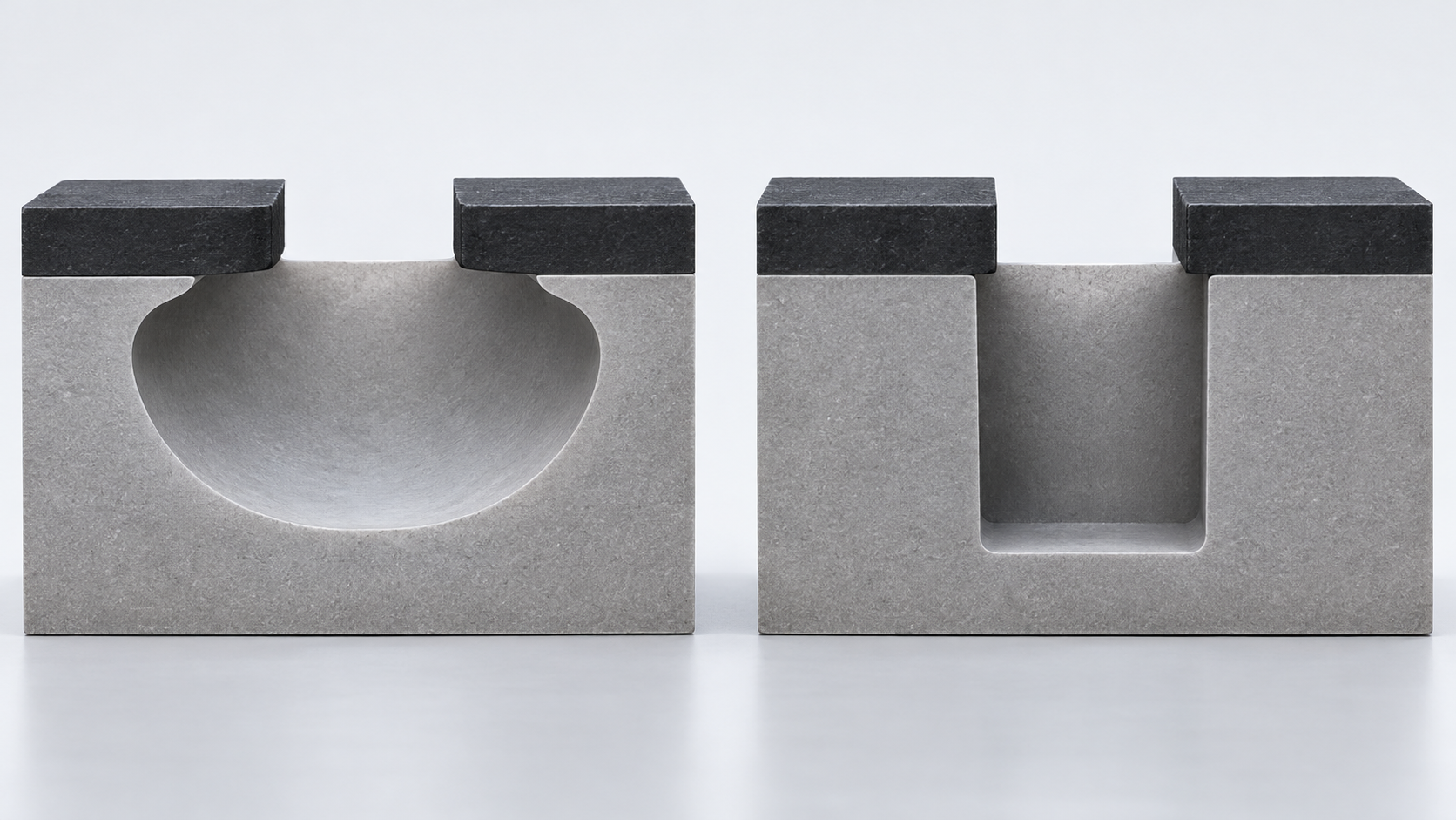
Shapes, colors and dimensions are illustrative. Consult the original schematic below for exact values and label correspondence.
View the original SVG schematic and exact annotations
Reading guide and original schematic labels: Wet and dry etching: isotropic and anisotropic (conceptual) / Cross-section sketch. The mask opening is the same; the way the film is removed differs. / Wet (liquid chemicals): isotropic / Chemicals (attack in every direction) / Etches sideways at the same / rate and undercuts the mask / Dry (plasma): anisotropic / Ions (arrive vertically) / Etches downward, keeping a shape / close to the mask opening / Mask (resist etc.) / Film to etch / Substrate / * Wet etching is generally isotropic and dry etching typically anisotropic, per the comparison table of Lee et al. [Source 1]. / * Real dry etching also has lateral (isotropic) components depending on conditions. Shapes and sizes are schematic.
3. What happens in the plasma: ions and radicals
The heart of dry etching is a plasma, an ionized gas. It contains charged ions and neutral, highly reactive radicals. Ions are accelerated by an electric field and strike the surface nearly vertically; radicals move in all directions and drive chemical reactions (this article's conceptual summary, interpreting the discussion of Donnelly and Kornblit and of Jeong et al.).
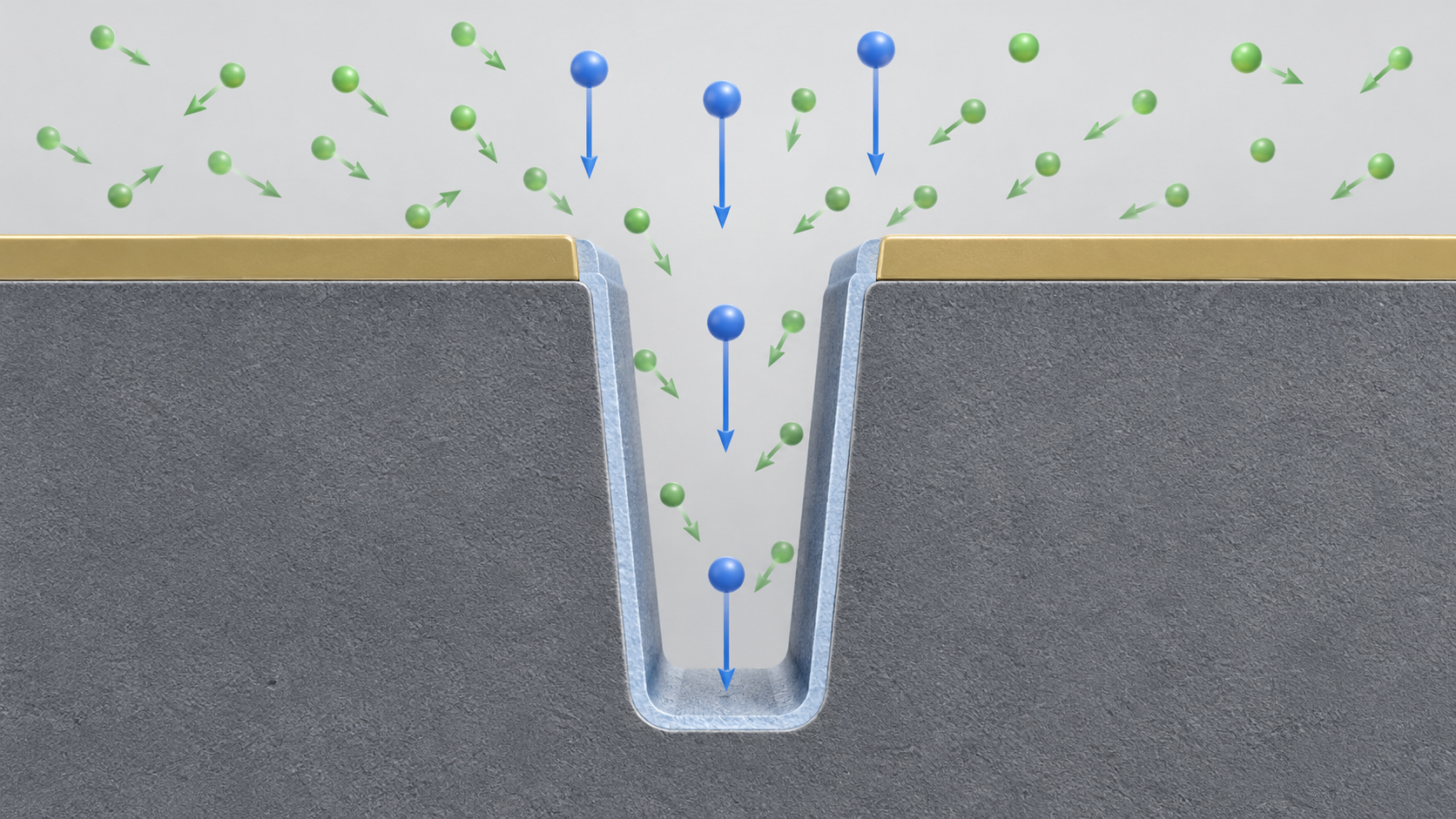
Shapes, colors and dimensions are illustrative. Consult the original schematic below for exact values and label correspondence.
View the original SVG schematic and exact annotations
Reading guide and original schematic labels: How reactive ion etching works: the roles of ions and radicals (conceptual) / Ions in the plasma are accelerated by an electric field and strike the surface nearly vertically. / Plasma (ionized gas) / Sheath (field accelerates ions) / From the mask opening to the trench bottom / Ions (red) / Accelerated by the field and / vertical; drive reaction at the bottom / Radicals (blue) / Neutral, moving in all directions; / the chemical workhorse (isotropic) / Protective film on walls and mask / A polymer film such as / fluorocarbon guards the walls / * Roles of ions, radicals and polymer protection: a concept drawn from Jeong et al. [Source 6] and Kim et al. [Source 7]. / * Ion angular distribution, film thickness and by-product desorption are omitted in this sketch.
Jeong et al. (2023, peer-reviewed; the authors include researchers from Samsung Electronics) studied high-aspect-ratio SiO2 etching in a dual-frequency capacitively coupled plasma (Ar/C4F8), controlling ion energy and flux individually to separate their contributions. In its introduction the paper says that high-aspect-ratio etching faces notching, bowing, twisting and tapering as well as aspect-ratio-dependent etching, and that the mechanisms are not well understoodSourced. Earlier work that the paper describes found that the neutral-to-ion flux ratio is key: at low ratios the etch rate rises with the ratio, while at high ratios a thick fluorocarbon film forms and the etch rate falls; and that fast neutrals formed by ions neutralized on sidewalls reach the bottom of a deep trench by Knudsen transport and can be the main etchantSourced (a description of earlier simulations and experiments).
A plasma is less a "cutting tool" than a source of reactive species (this article's commentary). Whether a film material can be etched is decided by whether a volatile reaction product forms. As we saw in our explainer on resists and photomasks, Li et al. improved the etchability of platinum by adding tungsten, which forms volatile products in fluorine plasmaSourced. In Kim et al.'s (2025) selective etching of SiGe over Si, XPS showed that in CF4/N2 a higher surface concentration of GeFx species promoted SiGe etching, while Si–N bonds inhibited etching of Si by fluorine radicalsSourced. So selectivity is, in substance, a design that makes volatile products form more easily on the film to cut than on the film to keep. The idea of "ion-neutral synergy" put forward by Coburn and Winters in 1979 (as introduced in a paper by Kanarik et al.) is an extension of thisSourced.
4. Selectivity and the mask: our calculation
Selectivity is the ratio of the etch rate of the film to cut to that of the mask (Lee et al. define it as "the ratio of etching rates between different materials")Sourced. If selectivity is low, the mask is gone before the deep cut is finished.
Looking only at mask consumption, we estimate the mask thickness needed as etch depth ÷ selectivityOur calculation.
- 100 nm deep: 50 nm at selectivity 2, 20 nm at 5, 10 nm at 10, 5 nm at 20. A thin EUV resist (about 35 nm, Hasan et al.'s review) therefore needs a selectivity of about 3 or more to cover 100 nm (100 ÷ 35 = about 2.9)
- 10 µm deep (the depth of a hole with aspect ratio about 100, Suda et al.): 1,000 nm at selectivity 10, 500 nm at 20, 200 nm at 50
Assumptions and limits: the selectivity values are this article's assumed examples, not those of a real process. Lateral recession of the mask, faceting (corner erosion) and the selectivity between mask and underlayer are not included. In real processes a hard-mask film (carbon-based, metal-based and so on) is generally stacked beneath the resist to secure the required thickness (this article's commentary; individual stacks were not checked here).
As we saw in our explainer on resists and photomasks, one strength of metal-oxide resists is high etch resistance. Hasan et al.'s review says metal-oxide resists withstand the etching that transfers the pattern into underlying layers betterSourced. The demand to cut deep with a thin resist is thus met from both the material side (a resist of high resistance) and the process side (a gas of high selectivity) (commentary).
5. Gas chemistry: fluorine-based and other combinations
The etch gas changes with the combination of film to cut and film to keep. Here are reported examples with their conditions.
| Target | Reported gas and conditions (level) | Features and aim | Source |
|---|---|---|---|
| High-aspect-ratio SiO2 etching | Ar/C4F8, dual-frequency capacitively coupled plasma (laboratory) | Fluorocarbon film thickness changes with the neutral-to-ion flux ratio | Jeong et al. (2023) |
| Aspect-ratio etching of SiO2 (low temperature) | CF4/H2/Ar, 200 nm trenches (laboratory) | Lower temperature raised the etch rate and aspect ratio and reduced necking and bowing | Kwon et al. (2024) |
| ONON stacks of SiO2/SiN (3D NAND) | HF with a phosphorus-containing gas, cryogenic, dual-frequency capacitively coupled plasma (laboratory) | Depth beyond 10 µm, aspect ratio about 100. Productivity reported to be greatly higher than conventional fluorocarbon processes | Suda et al. (2025) |
| SiNx (double patterning) | CHF3/CF4 formerly; C2H2F4/CF4O as an alternative (laboratory) | The old gases have low selectivity and high GWP. The alternative improved selectivity and removed trenching (through mixing) | Kim et al. (2025, Sci. Rep.) |
| Selective etching of SiGe over Si | CF4/N2, CF4/O2 (laboratory) | CF4/N2 gave better selectivity and profile. Si–N bonds suppressed Si etching | Kim et al. (2025, Materials) |
| SiO2/SiN stacks in 3D NAND (high aspect ratio) | C3HF5 (CF3CHCF2). A fundamental photoionization study (laboratory) | Described by the authors as a low-GWP candidate (GWP below 1) | Nguyen et al. (2025) |
All Sourced (statements in the papers). Films, conditions and levels differ, so this is not a ranking of gases.
Fluorocarbon gases create a polymer film that coats sidewalls and mask while etching. Kim et al. (2025, Sci. Rep.) report that C2H2F4 promoted stronger polymerization than CHF3, so mask protection improved but polymer deposition caused trenching (a dug-out groove bottom). Adding CF4O increased fluorine dissociation, reduced polymer, and eliminated the trenchingSourced. As the earlier work described by Jeong et al. shows, a film that is too thick lowers the etch rateSourced. So the balance between polymer deposition and etching is the core of gas design, the same view as "deposition and removal become parts of one process" in our explainer on atomic layer deposition (this article's commentary). The general trend that the carbon-to-fluorine ratio changes how readily a gas polymerizes was not confirmed here from individual primary sources.
6. Selective isotropic etching in three-dimensional transistors
In nanosheet structures such as gate-all-around (GAA), Si and SiGe are grown epitaxially in alternation and only the SiGe is etched away to leave stacked Si channels (Kim et al., 2025)Sourced. What is needed here is not vertical but lateral (isotropic) selective etching.
The paper by Kim et al. (2025, Materials, Yonsei University) lists the ways to etch SiGe selectively: wet etching (an earlier report of selectivity above 150 for 40 nm layers of Si0.76Ge0.24), thermal etching with HCl (needs more than 600 °C, risking dopant diffusion) and dry plasma etching. Wet etching has limits: SiGe may remain in the etch tunnel if oxidation is insufficient, and pattern collapse can occur on dryingSourced. The paper put a plate (a "roof") above the samples to block ion bombardment in CF4/N2 and CF4/O2 plasmas and examined the contribution of radicals alone. CF4/N2 was better in selectivity and profile, and reducing ion collisions raised selectivity furtherSourced (laboratory).
In vertical etching, ions were the stars. In lateral selective etching such as SiGe, ions are rather a nuisance, and the implication of this study is that chemical etching by radicals alone gives higher selectivity (this article's commentary). Even with "the same plasma", the ratio of ions to radicals is changed so that it is used anisotropically or isotropically. And if isotropic atomic layer etching (thermal ALE) can be used, it may combine selectivity with uniformity into deep structures (Section 8).
7. High-aspect-ratio etching (3D NAND)
In 3D NAND and similar devices, deep, narrow holes (memory holes) are opened through stacked films. Jeong et al. say that high-aspect-ratio etching suffers from notching, bowing, twisting, tapering and aspect-ratio-dependent etching (ARDE); that multi-frequency control, voltage waveform tailoring and pulse modulation have been developed to suppress these; and that the processes have become more complicated, with more steps and gas mixtures, so understanding of the mechanism lagsSourced.
Several examples of using temperature as a remedy have been reported.
- Low temperature (Kwon et al., 2024, Nanomaterials): in CF4/H2/Ar plasma on SiO2 in 200 nm trenches, a lower temperature raised the etch rate and aspect ratio and lowered the necking and bowing ratios. The authors suggest that the neutral species reaching the etch front have a low sticking coefficient and that directional ions are at workSourced (laboratory)
- Cryogenic HF-based (Suda et al., 2025, JVST B): ONON (silicon oxide/silicon nitride) holes were etched with HF and a phosphorus-containing gas, under cryogenic conditions, in a dual-frequency capacitively coupled plasma tool, demonstrating a depth beyond 10 µm and an aspect ratio of about 100. Analysis indicates that co-adsorption of the by-product H2O and the etchant HF at cryogenic temperature, and further enhancement of H2O adsorption by the phosphorus-containing species, are key to the higher etch rate. The authors say productivity improved greatly over conventional fluorocarbon processesSourced (laboratory)
From Suda et al.'s "depth beyond 10 µm and aspect ratio about 100" we back out the hole diameterOur calculation.
- Diameter ≈ depth ÷ aspect ratio = 10 µm ÷ 100 = about 100 nm (about 0.1 µm)
- From the previous calculation, cutting 10 µm with a mask of selectivity 20 needs a mask of about 500 nm (0.5 µm), five times the diameter
Assumptions and limits: the aspect ratio is a rounded figure ("about 100") given in the paper, and the diameter is a guide derived from it. The selectivity of 20 is this article's assumption, not a value from the paper.
In thin, deep holes, whether ions and neutrals reach the bottom and whether reaction products get out dominate (this article's commentary). In the earlier work described by Jeong et al., radicals entering from the entrance react with sidewalls and do not reach the bottom, while fast neutrals neutralized on the sidewalls do. Temperature changes the balance of adsorption and desorption at the surface. The lowering of temperature by Kwon et al. and the cryogenic work of Suda et al. are both designs of what stays on the surface and how much rather than of "the chemistry of the film". The thermal ALE review by Fischer et al. (2021) likewise describes a model in which, under non-saturating conditions, limits on reactant delivery and by-product removal in high-aspect-ratio structures can make etching anisotropic (depth-dependent)Sourced. From the materials side, the film that protects sidewalls, the resistance of the mask and the volatility of by-products are the three keys (commentary).
8. Atomic layer etching (ALE)
Kanarik et al. (2015, peer-reviewed) define ALE as a technique for removing thin layers by sequential reaction steps that are self-limiting, driven by the semiconductor industry as an alternative to continuous etching and seen as an essential counterpart to ALDSourced. The basic idea is to separate a step that changes just one surface layer from a step that removes only that layer.
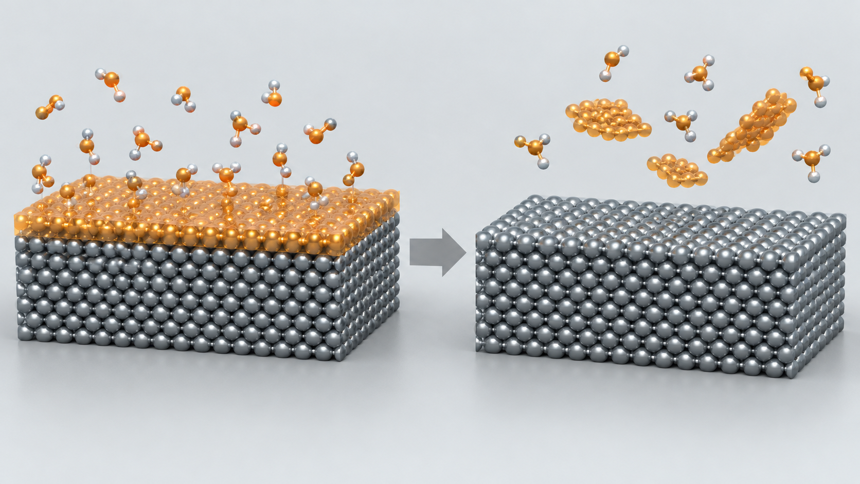
Shapes, colors and dimensions are illustrative. Consult the original schematic below for exact values and label correspondence.
View the original SVG schematic and exact annotations
Reading guide and original schematic labels: One cycle of atomic layer etching (ALE) (conceptual) / Two stages, changing just one surface layer and then removing only that layer, are repeated. / 1. Modify the surface / Reactive gas (red) / One surface layer changes / in a self-limiting way / 2. Purge / Excess gas is pumped out / 3. Remove the layer / Ion bombardment or heat / Only the modified layer / is volatilized and removed / 4. Purge / Surface one layer lower / By-products are pumped out; / on to the next cycle / Repeat steps 1 to 4 to remove a set amount / * Definition (self-limiting sequential reactions): Kanarik et al. [Source 3]. Removal: ions anisotropic, heat isotropic [Source 4]. / * Atom sizes, arrangement and the amount removed per cycle depend on the material; this is a conceptual diagram.
Removal comes in two modes. According to George (2020, peer-reviewed), plasma ALE releases the modified layer anisotropically by sputtering with energetic ions or neutrals, while thermal ALE releases it isotropically by thermal reactions of gas species and can be seen as "the reverse of ALD". The main thermal ALE mechanisms are fluorination and ligand exchange, common for metal oxides and nitrides, and conversion etchSourced. Fischer et al. (2021) organize thermal ALE of metals, metal oxides, metal nitrides, semiconductors and their oxidesSourced.
Kanarik et al. (2017) defined an "ALE synergy" parameter, describing how close a process is to ideal ALE, for plasma ALE of Si, Ge, C, W, GaN and SiO2, and reported that it scales with the surface binding energy of the material, which explains why some materials are more or less amenable to directional ALESourced. Kanarik et al. (2018, a peer-reviewed perspective) state that ALE is the most advanced etching technique in production today, that it was once considered too slow but that leveraging plasma has made it about a thousand times faster than earlier approaches, that prospects are better for strongly bound materials such as C, Ta, W and Ru, and they discuss an ALE smoothing effect (the surface flattens) and combining ALE and ALD for sub-10 nm challengesSourced (the authors' account).
Where ALD uses adsorption that "stops when saturated", ALE is two-staged: "modification that stops when saturated" plus "only the modified layer is removed" (this article's commentary). What matters is that the removal step responds only to the bonding of the modified layer and does not reach the unmodified layer below, which is what makes "one layer at a time" possible. As we saw in our explainer on atomic layer deposition, the correction steps of area-selective ALD include selective etching (Mackus et al.). So there is a direction in which ALD and ALE are switched within one tool and one recipe (Kanarik et al. also mention combining ALE and ALD). On the other hand, a cycle takes time, as with ALD, so it is natural to see ALE used where "a precise finish of the last few nanometres" is needed (commentary; how it is used in volume production was not confirmed here).
9. Gases and regulation: greenhouse gases and PFAS
A common problem is that the fluorine-based gases used for etching and CVD-chamber cleaning have large global warming potentials (GWP). Kim et al. (2025, Sci. Rep.) say that CHF3/CF4, formerly used for SiNx etching, have low selectivity and high GWP, which created the need for alternative gasesSourced.
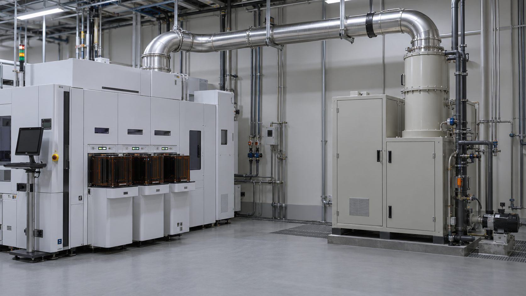
(1) Global warming potential (GWP): values differ by source
In Table A-1 of the US greenhouse gas reporting rule (40 CFR Part 98), the 100-year GWPs are 23,500 for SF6, 16,100 for NF3, 6,630 for CF4, 11,100 for C2F6 and 9,540 for c-C4F8, and 12,400 for trifluoromethane (HFC-23) (the version retrieved from the eCFR in October 2026)Sourced. The annexes of EU Regulation 2024/573 give the same gases as 7,380 for CF4, 12,400 for C2F6, 10,200 for c-C4F8, 24,300 for SF6 and 17,400 for NF3 (GWP 100, in the columns based on the Sixth Assessment Report)Sourced. Even within the same annex, the HFC section (14,800 for HFC-23) is based on the Fourth Assessment Report, so the edition of the assessment report is mixedSourced.
GWP expresses how many kilograms of CO2 a 1 kg release is equivalent to in warming. Calculating from the values aboveOur calculation:
- 1 kg of CF4 is equivalent to about 6,630 kg of CO2 in the US table and about 7,380 kg in the EU annex (a difference of about 11%: 7,380 ÷ 6,630 = 1.11)
- SF6 is about 3.5 times CF4 (23,500 ÷ 6,630; about 3.3 times with the EU values)
Assumptions and limits: the US table does not state the assessment-report edition, and we could not confirm it. GWP is a per-substance coefficient and does not include a fab's emissions (gas use, utilization efficiency and abatement efficiency), which we could not confirm from primary sources.
(2) The EU F-gas Regulation (Regulation (EU) 2024/573)
Regulation (EU) 2024/573, adopted on 7 February 2024 (published in the Official Journal on 20 February 2024 and in force on the twentieth day after publication), regulates fluorinated greenhouse gases and repealed Regulation (EU) No 517/2014Sourced. Its provisions on semiconductors are as follows.
- Labelling (Article 12): containers of fluorinated greenhouse gases in Annexes I and II placed on the market for etching of semiconductor material or cleaning of CVD chambers must be labelled for that purpose only. Article 12 applies from 1 January 2025Sourced
- HFC quota (Article 16): excluded from the quota that reduces HFCs placed on the market are HFCs supplied directly by a producer or importer to an undertaking using them for etching of semiconductor material or cleaning of CVD chambersSourced
- Review (Article 35): the review is to consider the potential inclusion of these HFCs (for semiconductor etching and CVD cleaning) in the quota. Whether to include them is undecidedNot yet confirmed
- Reporting: producers, importers and receiving undertakings must report quantities for this useSourced
(3) The EU PFAS restriction proposal (REACH)
According to ECHA's record (as of 9 October 2026): a proposal prepared by authorities in Denmark, Germany, the Netherlands, Norway and Sweden was submitted to ECHA on 13 January 2023 and published on 7 February 2023, with a consultation from 22 March to 25 September 2023. An updated proposal was published on 20 August 2025. The Risk Assessment Committee (RAC) adopted its final opinion on 2 March 2026, the Socio-Economic Analysis Committee (SEAC) agreed its draft opinion on 10 March, and a consultation on the draft ran until 25 May 2026. Both committees support an EU-wide restriction subject to specific derogations and recommend accompanying measures to minimize emissionsSourced. SEAC is expected to adopt its final opinion by the end of 2026, after which the European Commission is to propose a restriction based on the two final opinions, to be discussed and voted in the REACH Committee of Member StatesNot yet confirmed. As of now, no PFAS restriction has been adopted or put into application.
The summary of the updated dossier (October 2025, by KemI, the Swedish Chemicals Agency, and four other national authorities) includes semiconductor manufacturing (photolithography, etching, deposition, engineered fluids, equipment, advanced packaging, MEMS) in its "electronics and semiconductors" sector. For this sector, the assessment is that a full ban (RO1) is likely not proportionate, while a ban with time-limited derogations (RO2) and continued use with emission controls (RO3) are likely proportionate (the dossier submitters' assessment)Sourced. The specific derogation periods for semiconductor manufacturing could not be confirmed here.
(4) The PFAS definition and etch gases
The OECD (2021) defines PFASs as fluorinated substances that contain at least one fully fluorinated methyl or methylene carbon atom (without any H, Cl, Br or I attached); with a few noted exceptions, any chemical with a perfluorinated methyl group (–CF3) or methylene group (–CF2–) is a PFASSourced. The report states that HFC-23 (CHF3) and HFC-32 are not PFASs, because H remains on the carbonSourced.
This is this article's reading of that definition within what we read (not a legal judgment).
- SF6 and NF3: they contain no carbon, so they do not meet the OECD definition's "fluorinated carbon". Their GWP is large, however, and they are listed in the annexes of the EU F-gas Regulation
- CHF3: the OECD states it is not a PFAS. Its GWP is large (HFC-23)
- CF4, C2F6, c-C4F8: they contain fully fluorinated carbon, so they appear to meet the wording of the definition. How the EU proposal treats these individual substances was not confirmed here
- Low-GWP candidate gases (such as C3HF5): Nguyen et al. (2025) present C3HF5 (CF3CHCF2) as a candidate with GWP below 1. But it contains a CF3 group, so by the wording of the OECD definition it could be a PFAS. Choosing an alternative gas means looking at performance, GWP and PFAS status together
Because regulation arrives for "groups" of substances, developing alternative gases can have the structure that avoiding one regulation runs into another (commentary). It matters not to confuse the stage of the EU proposal (under consultation) with that of the F-gas Regulation (in force).
10. How to read the numbers: keep laboratory, source values, calculations and legal stages apart
| Number or item | What it is | Category | Caution |
|---|---|---|---|
| Depth beyond 10 µm, aspect ratio about 100 | Etching of ONON holes | Peer-reviewed paper (2025, laboratory) | A cryogenic HF/phosphorus-gas process. Not a production specification |
| About 35 nm | An example EUV resist thickness | Review (2024) | Varies by resist and process |
| Selectivity 2 to 50; 50 to 1,000 nm | Calculated mask thickness needed | Our calculation | Selectivities are assumed examples |
| About 1,000 times | How much faster plasma ALE became than earlier ALE | Perspective (2018, the authors' account) | Conditions and basis not checked here |
| GWP: CF4 6,630 / 7,380 | US table / EU annex (GWP 100) | Federal regulation and EU Regulation text | The assessment-report editions differ. Not emissions |
| 1 January 2025 | Start of application of F-gas Regulation Article 12 (container labelling) | EU Regulation (in force) | Labelling for semiconductor etching and CVD cleaning. Other provisions need separate checking |
| 2 March / 10 March / 25 May 2026 | PFAS proposal: RAC final opinion / SEAC draft opinion / end of consultation on the draft | ECHA record (under deliberation) | Not yet confirmed. Not adoption or application |
| End of 2026 | Expected adoption of SEAC's final opinion | ECHA's expectation | Not yet confirmed. A Commission proposal and a Member State vote follow |
11. Limits and what we could not confirm
(1) We could not confirm the gases and conditions used in volume production
Every gas example in this article is a laboratory report in a paper. The gases, temperatures, selectivities and etch rates of any particular company's or device's volume-production process could not be confirmed from primary sources.
(2) We could not confirm the specific derogations for semiconductor manufacturing in the PFAS proposal
The summary of the updated dossier gives the "electronics and semiconductors" sector and an overview of the assessment, but the specific periods and conditions of any derogation for semiconductor manufacturing could not be confirmed from the primary sources used here. Nor did we check which category individual gases (CF4, C4F8 and so on) fall into under the proposal.
(3) Regulation in the US, Japan, China, Korea and elsewhere is not covered
The regulation covered here is limited to the EU F-gas Regulation and PFAS restriction proposal and the GWP table in a US reporting rule. Voluntary emission-reduction commitments and national PFAS rules are not covered.
(4) We could not confirm abatement or gas utilization
Actual emissions depend on gas use, utilization in the reaction and abatement efficiency. We could not confirm these numbers from primary sources.
(5) We could not confirm how ALE is used in volume production
Kanarik et al. call it "the most advanced etching technique in production today" (2018), but we have not checked which steps use it and to what extent.
- Wet etching is isotropic and dry etching typically anisotropic. Plasma made vertical etching possible and underpinned shrinkingSourced
- Ions work vertically and radicals do the chemistry. A polymer film protects sidewalls but stops etching if too thickSourced
- Cutting deep through a thin mask needs high selectivity. By our calculation a 10 µm deep hole at aspect ratio about 100 is about 100 nm acrossOur calculation
- Temperature is the key in high aspect ratios. A cryogenic HF-based process has been reported beyond 10 µm depth at aspect ratio about 100 (laboratory)Sourced
- ALE is a two-stage self-limiting process; plasma ALE is anisotropic and thermal ALE isotropic. It is ALD's counterpartSourced
- The F-gas Regulation is in force and the PFAS restriction proposal is under deliberation. GWP values differ by source, and a low-GWP gas can still meet the wording of the PFAS definitionNot yet confirmed
12. Glossary
- Etching
- The step that selectively removes the film the mask does not protect.
- Wet / dry
- Cutting with liquid chemicals / with plasma or gas in vacuum.
- Isotropic / anisotropic
- Etching at the same rate in every direction / only in a particular (vertical) direction.
- Selectivity
- The ratio of the etch rates of the target film and the mask (or underlayer).
- RIE
- Reactive ion etching. Dry etching that uses ions and radicals together.
- Radical
- An uncharged, highly reactive species. The chemical workhorse.
- ARDE
- Aspect-ratio-dependent etching. The etch rate falls as holes get deeper.
- Bowing / necking / tapering / twisting
- A bulge partway down a hole / a narrowing at the entrance / narrowing toward the bottom / a tilt or twist.
- ALE
- Atomic layer etching. Removing material one layer at a time by self-limiting sequential reactions.
- Thermal ALE
- ALE that removes the modified layer isotropically by gas thermal reactions; "the reverse of ALD".
- GWP
- Global warming potential. Warming strength relative to the same mass of CO2.
- PFAS
- Under the OECD definition, substances with a fully fluorinated methyl or methylene carbon.
- RAC / SEAC
- ECHA's Risk Assessment Committee / Socio-Economic Analysis Committee.
- REACH
- The EU regulation on the registration, evaluation, authorisation and restriction of chemicals.
13. References (primary sources)
- Lee T et al. "Advances in core technologies for semiconductor manufacturing: applications and challenges of atomic layer etching, neutral beam etching and atomic layer deposition", Nanoscale Adv. 7(10), 2796–2817 (2025, peer-reviewed review, open access) — doi.org/10.1039/d4na00784k
- Hasan MW et al. "Recent Advances in Metal-Oxide-Based Photoresists for EUV Lithography", Micromachines 15(9), 1122 (2024, peer-reviewed review) — doi.org/10.3390/mi15091122
- Kanarik KJ et al. "Overview of atomic layer etching in the semiconductor industry", J. Vac. Sci. Technol. A 33(2), 020802 (2015, peer-reviewed review) — doi.org/10.1116/1.4913379
- George SM "Mechanisms of Thermal Atomic Layer Etching", Acc. Chem. Res. 53(6), 1151–1160 (2020, peer-reviewed) — doi.org/10.1021/acs.accounts.0c00084
- Donnelly VM, Kornblit A "Plasma etching: Yesterday, today, and tomorrow", J. Vac. Sci. Technol. A 31(5), 050825 (2013, peer-reviewed review) — doi.org/10.1116/1.4819316
- Jeong W et al. "Contribution of Ion Energy and Flux on High-Aspect Ratio SiO2 Etching Characteristics in a Dual-Frequency Capacitively Coupled Ar/C4F8 Plasma: Individual Ion Energy and Flux Controlled", Materials 16(10), 3820 (2023, peer-reviewed, open access) — doi.org/10.3390/ma16103820
- Kim K et al. "Effect of C2H2F4/CF4O with low global warming potentials on SiNx etching as a CHF3 replacement", Sci. Rep. 15, 40517 (2025, peer-reviewed, open access) — doi.org/10.1038/s41598-025-24378-w
- Kwon H et al. "Necking Reduction at Low Temperature in Aspect Ratio Etching of SiO2 at CF4/H2/Ar Plasma", Nanomaterials 14(2), 209 (2024, peer-reviewed, open access) — doi.org/10.3390/nano14020209
- Suda R et al. "Development for high-aspect-ratio hole etching with hydrogen fluoride gas based cryogenic process", J. Vac. Sci. Technol. B 43(6), 062210 (2025, peer-reviewed) — doi.org/10.1116/6.0005035
- Kim J et al. "Selective Etching of Multi-Stacked Epitaxial Si1-xGex on Si Using CF4/N2 and CF4/O2 Plasma Chemistries for 3D Device Applications", Materials 18(18), 4417 (2025, peer-reviewed, open access) — doi.org/10.3390/ma18184417
- Nguyen TQ et al. "Valence fragmentation dynamics of a promising low global warming etching gas CF3CHCF2", Sci. Rep. 15, 9507 (2025, peer-reviewed, open access) — doi.org/10.1038/s41598-025-94119-6
- Kanarik KJ, Tan S, Gottscho RA "Atomic Layer Etching: Rethinking the Art of Etch", J. Phys. Chem. Lett. 9(16), 4814–4821 (2018, peer-reviewed perspective) — doi.org/10.1021/acs.jpclett.8b00997
- US Code of Federal Regulations (eCFR) 40 CFR Part 98, Subpart A, Table A-1, "Global Warming Potentials, 100-Year Time Horizon" (the version retrieved from the eCFR API in October 2026) — ecfr.gov
- European Parliament and Council "Regulation (EU) 2024/573 of 7 February 2024 on fluorinated greenhouse gases", OJ L, 20.2.2024 — eur-lex.europa.eu
- OECD "Reconciling Terminology of the Universe of Per- and Polyfluoroalkyl Substances: Recommendations and Practical Guidance", OECD Series on Risk Management of Chemicals (July 2021, PDF) — doi.org/10.1787/e458e796-en
- ECHA "ECHA supports PFAS restriction with targeted derogations", news release ECHA/NR/26/17, 26 March 2026 — echa.europa.eu
- ECHA "Per- and polyfluoroalkyl substances (PFAS)", topic page (list of milestones), accessed 9 October 2026 — echa.europa.eu
- KemI (Swedish Chemicals Agency) and four other national authorities "What you need to know about the updated PFAS restriction dossier", updated 23 October 2025 (PDF) — kemi.se
- Fischer A et al. "Thermal atomic layer etching: A review", J. Vac. Sci. Technol. A 39(3), 030801 (2021, peer-reviewed review) — doi.org/10.1116/6.0000894
- Kanarik KJ et al. "Predicting synergy in atomic layer etching", J. Vac. Sci. Technol. A 35(5), 05C302 (2017, peer-reviewed) — doi.org/10.1116/1.4979019
- Li Z et al. "Evaluating an alternative Pt-W alloy as a low-n EUV mask absorber: Film properties and imaging performance", iScience 29(8), 116912 (2026, peer-reviewed, open access) — doi.org/10.1016/j.isci.2026.116912
14. Claim-to-source audit
| Claim in the text | Basis | Label |
|---|---|---|
| The comparison of wet and dry etching (wet: low cost, easy, high selectivity, isotropic, hard for sub-1 µm size, contamination, hard to hold etch rate; dry: deep, fast, automatable, can define sub-100 nm, typically anisotropic, poor selectivity, low throughput, toxic and corrosive gases, radiation damage), etch depth, profile, roughness and uniformity as controlled items, the definition of selectivity, and the place of ALE and NBE | Lee et al. (2025, peer-reviewed review, open access) [Source 1] https://doi.org/10.1039/d4na00784k | Sourced |
| That EUV resists are thin films of about 35 nm, and that metal-oxide resists have high etch resistance | Hasan et al. (2024, peer-reviewed review) [Source 2] https://doi.org/10.3390/mi15091122 | Sourced |
| The definition of ALE (removing thin layers by sequential self-limiting reactions) and its being seen as the essential counterpart to ALD | Kanarik et al. (2015, abstract of the peer-reviewed review) [Source 3] https://doi.org/10.1116/1.4913379 | Sourced |
| Plasma ALE (sputtering by ions and so on; anisotropic) and thermal ALE (gas thermal reactions; isotropic; the reverse of ALD), and the thermal ALE mechanisms (fluorination and ligand exchange, conversion etch) | George (2020, abstract of the peer-reviewed paper) [Source 4] https://doi.org/10.1021/acs.accounts.0c00084 | Sourced |
| That plasma etching was introduced in the mid 1960s to cut liquid waste and obtain selectivities hard to get with wet etching, and that anisotropic etching of Si, Al and SiO2 allowed about 40 years of shrinking | Donnelly and Kornblit (2013, abstract of the peer-reviewed review) [Source 5] https://doi.org/10.1116/1.4819316 | Sourced |
| Individual control of ion energy and flux in a dual-frequency capacitively coupled Ar/C4F8 plasma; the challenges of high-aspect-ratio etching (notching, bowing, twisting, tapering, ARDE) and growing complexity; and the earlier work described (neutral-to-ion flux ratio, a thick fluorocarbon film lowering the etch rate, Knudsen transport of fast neutrals) | Jeong et al. (2023, peer-reviewed, open access). The earlier-work part is the paper's introduction [Source 6] https://doi.org/10.3390/ma16103820 | Sourced |
| That CHF3/CF4 were used for SiNx etching with low selectivity and high GWP, and the alternative C2H2F4/CF4O (better selectivity; stronger polymerization protects the mask but causes trenching, removed by adding CF4O) | Kim et al. (2025, Sci. Rep., peer-reviewed, open access). Laboratory [Source 7] https://doi.org/10.1038/s41598-025-24378-w | Sourced |
| That lowering the temperature in CF4/H2/Ar for SiO2 in 200 nm trenches raised the etch rate and aspect ratio and lowered the necking and bowing ratios | Kwon et al. (2024, peer-reviewed, open access). Laboratory [Source 8] https://doi.org/10.3390/nano14020209 | Sourced |
| That a cryogenic HF plus phosphorus-containing gas process etched ONON holes beyond 10 µm deep at an aspect ratio of about 100, that co-adsorption of H2O and HF is key, and that productivity greatly improved over conventional fluorocarbon processes | Suda et al. (2025, abstract of the peer-reviewed paper). Laboratory [Source 9] https://doi.org/10.1116/6.0005035 | Sourced |
| SiGe/Si selective etching: wet selectivity above 150 (an earlier report) and its limits; HCl thermal etching above 600 °C; CF4/N2 better than CF4/O2 in selectivity and profile; fewer ion collisions raising selectivity; the roles of GeFx species and Si–N bonds | Kim et al. (2025, Materials, peer-reviewed, open access). Laboratory [Source 10] https://doi.org/10.3390/ma18184417 | Sourced |
| That C3HF5 (CF3CHCF2) is described by the authors as a low-GWP (below 1) etching gas candidate for high-aspect-ratio SiO2/SiN stacks in 3D flash | Nguyen et al. (2025, peer-reviewed, open access). A fundamental photoionization study [Source 11] https://doi.org/10.1038/s41598-025-94119-6 | Sourced |
| That ALE is the most advanced etching technique in production today, that plasma made it about 1,000 times faster, the smoothing effect, the combination with ALD, and better prospects for strongly bound materials such as C, Ta, W and Ru | Kanarik et al. (2018, abstract of the peer-reviewed perspective). The authors' account [Source 12] https://doi.org/10.1021/acs.jpclett.8b00997 | Sourced |
| The 100-year GWPs in Table A-1 of 40 CFR Part 98 (SF6 23,500; NF3 16,100; CF4 6,630; C2F6 11,100; c-C4F8 9,540; HFC-23 12,400) | US Code of Federal Regulations (retrieved from the eCFR in October 2026). The table does not state the assessment report [Source 13] https://www.ecfr.gov/current/title-40/part-98/subpart-A/appendix-Table%20A-1%20to%20Subpart%20A%20of%20Part%2098 | Sourced |
| Regulation (EU) 2024/573 (adopted 7 February 2024, published 20 February 2024, in force on the twentieth day after publication, repealing Regulation 517/2014); the labelling in Article 12 (containers for semiconductor etching and CVD chamber cleaning; applies from 1 January 2025); the exclusion from the HFC quota in Article 16; reporting duties; the Annex GWPs (CF4 7,380; C2F6 12,400; c-C4F8 10,200; SF6 24,300; NF3 17,400, from the columns based on the Sixth Assessment Report); and the HFC section based on the Fourth Assessment Report | The text of the EU Regulation (Official Journal) [Source 14] https://eur-lex.europa.eu/eli/reg/2024/573/oj/eng | Sourced |
| That the Article 35 review is to consider including HFCs for semiconductor etching and CVD cleaning in the quota (whether to include is undecided) | The Article 35 wording of the EU Regulation. The outcome is undecided [Source 14] https://eur-lex.europa.eu/eli/reg/2024/573/oj/eng | Not yet confirmed |
| The PFAS definition (a substance containing at least one fully fluorinated methyl or methylene carbon atom), and that HFC-23 and HFC-32 are not PFAS because H remains on the carbon | OECD (2021) [Source 15] https://doi.org/10.1787/e458e796-en | Sourced |
| The course of the PFAS restriction proposal (submitted 13 January 2023; published 7 February; consultation 22 March to 25 September 2023; updated proposal 20 August 2025; RAC final opinion adopted 2 March 2026; SEAC draft opinion 10 March; consultation on it until 25 May; SEAC final opinion expected by end of 2026; then a Commission proposal and a REACH Committee vote) | ECHA news and topic page (as of 9 October 2026). Under deliberation; not adopted or in force [Source 16] https://echa.europa.eu/-/echa-supports-pfas-restriction-with-targeted-derogations [Source 17] https://echa.europa.eu/hot-topics/perfluoroalkyl-chemicals-pfas | Not yet confirmed |
| That the "electronics and semiconductors" sector of the updated dossier summary includes semiconductor manufacturing (photolithography, etching, deposition, engineered fluids, equipment, advanced packaging, MEMS), and the dossier submitters' assessment that RO1 is likely not proportionate while RO2 and RO3 are likely proportionate | Summary by KemI and four other national authorities (updated 23 October 2025). The submitters' assessment [Source 18] https://www.kemi.se/download/18.64e3bd9619a0f45982cfff/1761213262828/What%20you%20need%20to%20know%20about%20the%20updated%20PFAS%20restriction%20dossier-Updated-2025-10-23.pdf | Sourced |
| The thermal ALE review: a model in which, in non-saturation mode, etch anisotropies from limits on reactant delivery and by-product removal can arise in high-aspect-ratio structures | Fischer et al. (2021, abstract of the peer-reviewed review) [Source 19] https://doi.org/10.1116/6.0000894 | Sourced |
| The definition of ALE synergy (plasma ALE of Si, Ge, C, W, GaN and SiO2), that it scales with surface binding energy, and Coburn and Winters' 1979 idea of ion-neutral synergy | Kanarik et al. (2017, abstract of the peer-reviewed paper) [Source 20] https://doi.org/10.1116/1.4979019 | Sourced |
| That adding tungsten to platinum creates volatile products in fluorine plasma and improves etchability | Li et al. (2026, peer-reviewed, open access) [Source 21] https://doi.org/10.1016/j.isci.2026.116912 | Sourced |
| Required mask thickness by selectivity (100 nm depth: 50, 20, 10, 5 nm at selectivity 2, 5, 10, 20; selectivity of about 3 or more for the thin 35 nm resist, 100÷35 = about 2.9; 10 µm depth: 1,000, 500, 200 nm at selectivity 10, 20, 50); hole diameter ≈ 10 µm÷100 = about 100 nm; and GWP ratios (7,380÷6,630 = 1.11 for CF4; SF6/CF4 = 3.5 [US] and 3.3 [EU]) | Our calculation. Selectivities are assumed examples. Mask recession, faceting and underlayer selectivity are not included. GWPs are the sources' values | Our calculation |
| The framing of the roles of ions and radicals in plasma; volatile products as the content of selectivity; the balance of polymerization and etching as the heart of gas design; the reading that fewer ions raise selectivity in lateral selective etching; high aspect ratio as a design of transport and adsorption/desorption; the place of ALE; integration with ALD; applying the PFAS definition to SF6, NF3, CHF3, CF4 and similar gases and low-GWP gases (not a legal judgment); and each materials-engineer box | This article's organization and commentary based on the published content. The general trend of C/F ratio and polymerization, whether individual gases fall under PFAS rules, and the cause of each profile distortion were not individually confirmed | Commentary |
| The gases and conditions used in volume production, the specific derogations for semiconductor manufacturing, regulation in the US, Japan, China and Korea, abatement and gas utilization, and how ALE is used in volume production | Could not be confirmed from primary sources within the scope of this article, so not stated | Commentary |
| That Figs. 2 to 6 and 8 are explanatory drawings, not real design or measurement drawings, and that Figs. 1 and 7 are AI-generated images | This article's note | Commentary |
Last updated: 9 October 2026 / Sources are limited to primary material (peer-reviewed papers, EU and US federal regulations, and official documents of the OECD, ECHA and others). Because structural readings and materials-design interpretations are included, they are marked as "Commentary" and kept apart from sourced facts. Gases and conditions used in volume production, the specific PFAS derogations for semiconductor manufacturing, regulation in other countries, abatement and how ALE is used in volume production could not be confirmed, so they are not stated. Regulation is written with the stages kept apart: the F-gas Regulation (in force) and the PFAS restriction proposal (under deliberation; not adopted or in force). Whether a gas falls under PFAS is not a legal judgment but this article's reading of the OECD definition. The figures are explanatory diagrams. Figs. 2 to 6 and 8 are vector drawings and Figs. 1 and 7 are AI-generated images; none of them shows an actual photograph or design of a tool, process or facility.