TECHNOLOGY EXPLAINER
Lithography and EUV
— shorten the wavelength 14-fold, and now there are too few photons
Chip circuits are drawn with light. The smallest line you can print is set, to a first approximation, by k1 × wavelength ÷ NA. When ArF immersion (193 nm) neared its limit, the industry moved to EUV (extreme ultraviolet) light at 13.5 nm. The light source is a plasma made by hitting molten tin droplets with a laser, and because nothing is transparent at that wavelength there are no lenses, only mirrors. This article explains how it works, and how having less light, and fewer photons, creates the next set of problems, keeping the origin of each number clearly apart.
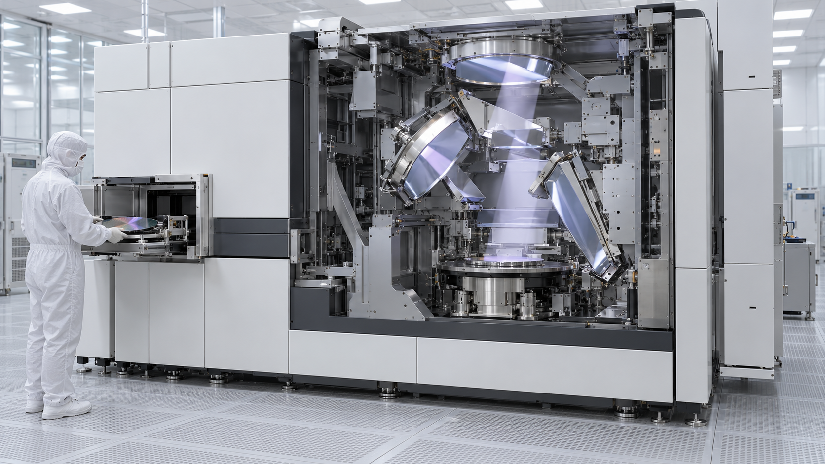
- What lithography and EUV are (the short version)
- The resolution equation: wavelength, NA and k1
- Our calculation: working k1 back from published minimum feature sizes
- ArF immersion: keeping 193 nm and raising NA to 1.35
- Multiple patterning: going past the optical limit with deposition and etch
- EUV: 13.5 nm light does not pass through lenses
- The source: hitting molten tin with a laser
- Mirrors: ten reflections leave about 2% of the light
- Our calculation: photon counts, where a shorter wavelength means fewer photons per unit energy
- Pellicles and masks (overview)
- High-NA EUV: NA 0.55, 8 nm
- How to read the numbers
- Limits and what we could not confirm / Glossary / Primary sources / Claim-to-source audit
Sourced = a value stated in published material (link given)
Our calculation = a figure this article derived, with the assumptions spelled out
Not yet confirmed = a plan or target with no confirmed track record
Structural readings and materials-design interpretations are marked separately as Commentary.
Equipment makers' figures are labelled manufacturer's stated value, and always come with the condition they were stated for (illumination, pattern, dose). We do not present a laboratory best result as the performance of a production tool.
This is an explainer on the principles and evaluation of semiconductor manufacturing tools and materials. It does not rank any company, tool or country. Equipment makers' numbers are their own stated values and are distinct from results at customers' fabs.
1. What lithography and EUV are (the short version)
Lithography (exposure) is the step in which light passes through an original carrying the circuit pattern (the reticle), is reduced in size, and is imaged onto a light-sensitive film (resist) on the wafer. The relief left after development becomes the template for the next step, etching or deposition.
- The wavelength has kept getting shorter: ASML describes the progression from mercury lamps at 436 nm (g-line) and 365 nm (i-line) to excimer lasers, KrF at 248 nm and ArF at 193 nm. EUV uses 13.5 nm, which it says is more than 14 times shorter than DUV lightSourced
- EUV is a different world of equipment: EUV light is absorbed by almost every material, so lenses cannot be used; multilayer mirrors work in a vacuum. The source is a plasma made by hitting molten tin droplets with lasers (ASML)Sourced
- Only ASML builds EUV scanners: ASML's Form 20-F for 2025 says it is currently the world's only manufacturer of EUV lithography systemsSourced. This article is not an assessment of any company; it covers how the technology works and how to read the numbers
A shorter wavelength lets you print finer lines, but materials absorb the light, and less of it gets from the source to the wafer. In an EUV tool with ten mirror reflections, only about 2% of the light reaches the wafer (an estimate by Fomenkov et al.)Sourced. And because each photon carries more energy, the same energy delivers far fewer photonsOur calculation. This scarcity of light feeds into resist sensitivity and stochastic defects (see our explainer on resists and photomasks in this series).
This series covers nanoscale fabrication in chipmaking across four articles: this one (drawing the pattern), then resists and photomasks (the light-sensitive film and the original), atomic layer deposition (building films one atomic layer at a time), and etching (cutting). Methods that transfer a pattern without light, such as nanoimprint, are covered in our explainer on self-assembly and nanoimprint.
2. The resolution equation: wavelength, NA and k1
ASML explains the smallest printable dimension (CD, critical dimension) with the following equation, known as the Rayleigh criterionSourced.
λ: exposure wavelength. NA: numerical aperture, a number describing how wide a cone of light the optics can collect. k1: a coefficient set largely by process tricks; ASML gives its physical limit as k1 = 0.25Sourced.
The equation leaves three routes to a smaller feature. ASML frames them as shortening the wavelength (a major technology shift), increasing NA, and reducing k1 (through illumination and computational lithography)Sourced.
| Lever | What you do | Cost and difficulty (commentary) |
|---|---|---|
| Shorten wavelength λ | Replace the source, optical materials and resist (ASML: a new wavelength needs new light sources, optical materials and resists) | Biggest step forward, but everything is rebuilt. At EUV, materials absorb the light |
| Raise NA | Build larger, more precise optics. ArF immersion puts water between lens and wafer for NA 1.35; High-NA EUV uses 0.55 | Optics grow huge and costly. The depth over which the image stays in focus (DOF) shrinks (Section 11) |
| Lower k1 | Off-axis illumination, tailored pupil shapes, correction of the original pattern (OPC) | 0.25 is the limit. The closer you get, the smaller the process window (tolerance to variation) |
The first half of "What you do" is ASML's explanation [Sources 1, 3, 4]: Sourced. The right-hand column is this article's commentary.
3. Our calculation: working k1 back from published minimum feature sizes
We take the wavelength, NA and minimum feature size that ASML states on its product pages (manufacturer's stated values) and invert the equation: k1 = CD × NA ÷ λOur calculation.
- ArF immersion (NXT:2000i): λ = 193 nm, NA = 1.35. ASML lists production resolution of 40 nm (C-quad illumination) and 38 nm (dipole). k1 = 38 × 1.35 ÷ 193 = 0.266; for 40 nm, 0.280
- EUV 0.33 NA (NXE:3800E): λ = 13.5 nm, NA = 0.33, resolution listed as 13 nm. k1 = 13 × 0.33 ÷ 13.5 = 0.318
- High-NA EUV (EXE:5000): NA = 0.55, resolution listed as 8 nm. k1 = 8 × 0.55 ÷ 13.5 = 0.326
Assumptions and limits: which feature the CD refers to (dense half-pitch or something else), the illumination, the resist and the tolerated variation are not stated on the product pages. This k1 is therefore a rough figure back-calculated mechanically from stated numbers, not the k1 of any actual process. That the ArF value sits closer to 0.25 than the EUV values reflects how immersion makes up for its longer wavelength with illumination tricks (this article's commentary).
4. ArF immersion: keeping 193 nm and raising NA to 1.35
The mainstay before EUV is the 193 nm ArF excimer laser with immersion. ASML says that in 2003 it developed immersion lithography, which projects light through a layer of water between the lens and the wafer; without the water, an NA above 1 was impossible, and with it its optics reach NA 1.35Sourced. Lin (2004, peer-reviewed) describes water immersion as effectively shortening the 193 nm wavelength to 135 nmSourced. The ratio 193 ÷ 135 = about 1.43 corresponds to the refractive index of waterOur calculation.
According to ASML, the optics of its highest-resolution DUV machines stand more than 1.2 m tall and weigh over a tonne. The NXT:2000i is designed for 4× reduction, a 26 × 33 mm field and compatibility with existing reticles, and the page cites a champion productivity of 4,600 wafers per day (manufacturer's stated value)Sourced.
In immersion, the thin water layer between lens and wafer must not form bubbles or leave drying marks even as the wafer moves at high speed. For the resist surface in contact with water, that means either a water-repellent protective film (topcoat) or a resist designed to be water-repellent so that components do not leach into the water and droplets do not linger (commentary; we did not confirm specific materials or specifications within the scope of this article). What looks like an "optics" story is, on the materials side, a story of interface design between water and resist, which governs tool productivity (scan speed). ASML's statement on the NXT:2050i page that a new immersion hood reduces water loss and significantly improves defectivity [Source 15] also shows that water handling sits at the center of performanceSourced.
5. Multiple patterning: going past the optical limit with deposition and etch
ASML's stated production resolution for the NXT:2000i is 38 nm with dipole illumination and 40 nm with C-quad [Source 5]Sourced. Lines finer than that cannot be drawn in one exposure, so exposure is combined with deposition and etch and repeated. This is multiple patterning. The background section of a Tokyo Electron US patent (US 11,676,817 B2) says that multiple patterning has extended 193 nm immersion lithography to patterned layers with a pitch of less than 30 nm, and that self-aligned approaches (sidewall image transfer, SIT) grew out of the overlay-error problem of combining two exposures (this is the patent's description; we do not interpret its claims)Sourced.
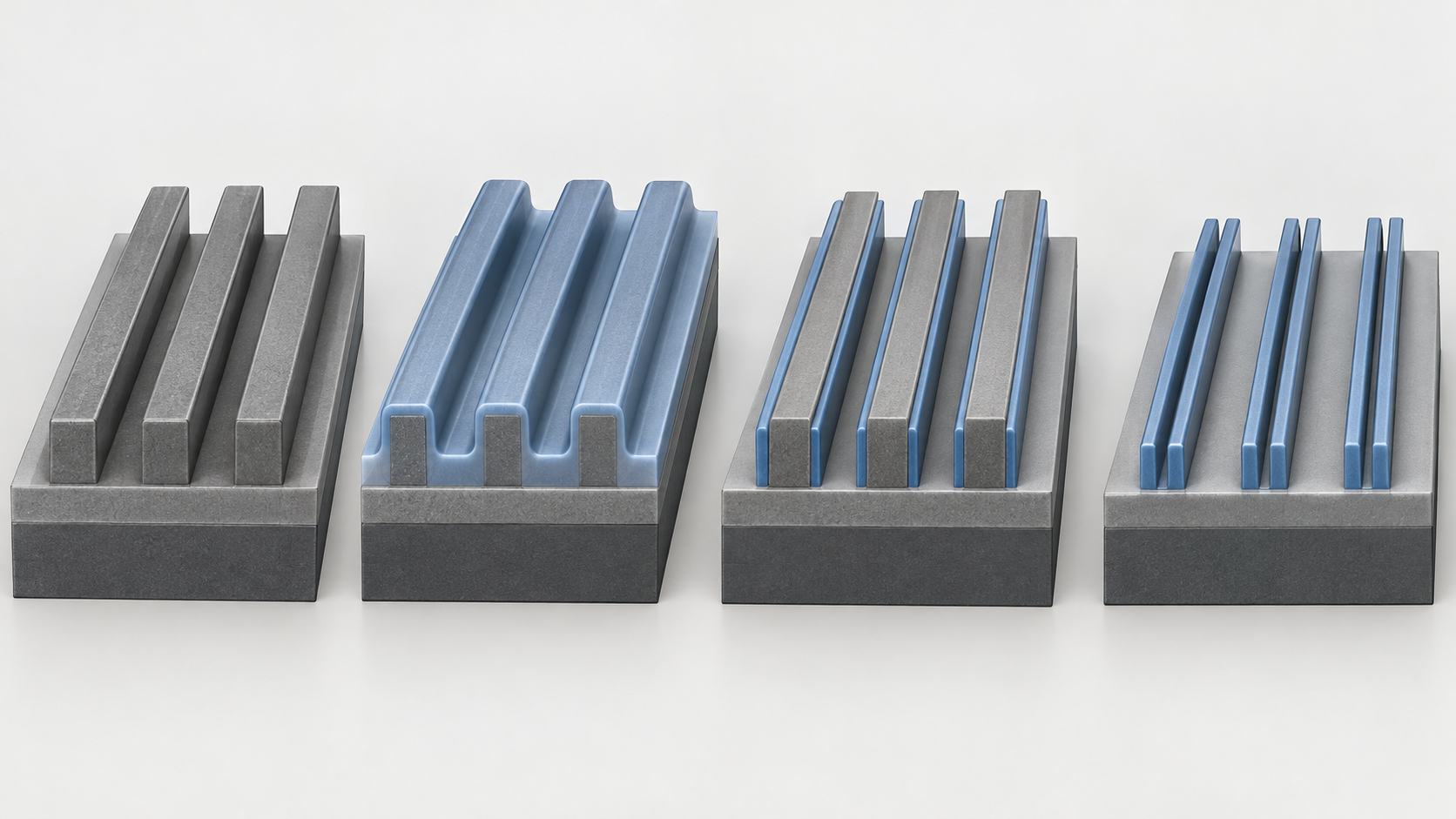
Shapes, colors and dimensions are illustrative. Consult the original schematic below for exact values and label correspondence.
View the original SVG schematic and exact annotations
Reading guide and original schematic labels: Self-aligned double patterning (SADP) flow (conceptual) / Cross-section sketch. No dimensions; it shows only that when mandrel width equals spacer thickness, the pitch halves. / 1. Expose and develop: form mandrels at the minimum pitch P / Pitch P / 2. Deposit: lay a thin, uniform film over the mandrels (see atomic layer deposition) / 3. Anisotropic etch: remove top and bottom film, leaving sidewall film (spacers); see etching / 4. Remove the mandrels selectively: the gap between spacers is P ÷ 2 / Pitch P ÷ 2 / * Blue = mandrel, orange = spacer film, grey = substrate. Outline follows US 11,676,817 B2 [Source 14]. / * Repeating gives SAQP, with one quarter of the minimum pitch. Layer shapes are schematic.
In its 2025 Form 20-F, ASML describes the aim of EUV as moving from complex multi-patterning to single patterning, with one exposure per layer, which reduces the number of masks and process steps and improves yield and scalabilitySourced.
Step 2 in Fig. 4 puts a film of uniform thickness on the sides and the top of each mandrel, and its thickness accuracy becomes line-width accuracy directly. Step 3 is an anisotropic etch that removes only the horizontal surfaces, leaving the sidewalls, and step 4 etches away only the mandrel selectively. The tools that carry you past the optical limit are therefore ALD and etch, and the materials issues become film-thickness uniformity, selectivity against the underlayer and sidewall profile (this article's commentary; see our explainers on atomic layer deposition and etching in this series). Even if the number of exposures does not rise, the number of deposition, etch and clean steps does, and with it the number of places defects can enter. The reason EUV single exposure is said to "reduce steps" is that it breaks this chain (commentary consistent with ASML's description).
6. EUV: 13.5 nm light does not pass through lenses
ASML describes EUV lithography as using light at 13.5 nm, more than 14 times shorter than DUVSourced (193 ÷ 13.5 = about 14.3Our calculation). Shrinking λ by that factor is a large gain: ASML explains that although the NA of EUV (0.55) is lower than the 1.35 of DUV, EUV prints smaller features because it uses a much shorter wavelengthSourced.
The price is that almost every material absorbs EUV. ASML states that there are no lenses for EUV, since most materials absorb the light, and that it instead uses ultrasmooth multilayer mirrors inside a vacuum chamberSourced. Each mirror has more than 100 layers engineered to maximize EUV reflection and is polished to a smoothness of less than one atom's thicknessSourced.
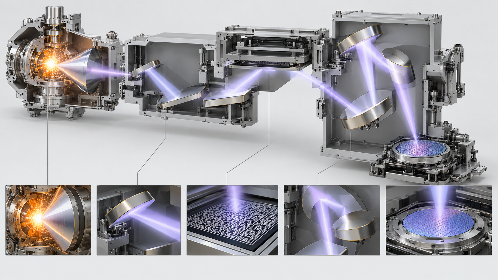
Shapes, colors and dimensions are illustrative. Consult the original schematic below for exact values and label correspondence.
View the original SVG schematic and exact annotations
Reading guide and original schematic labels: The light path of an EUV scanner (conceptual) / All in vacuum. No lenses; light is guided by reflection only. / Source (making the EUV) / Tin droplet generator / about 25 µm across / ejected at 70 m/s / 50,000 per second / CO2 laser / weak pulse flattens / the droplet, a strong / pulse vaporizes it / Tin plasma / emits EUV at 13.5 nm / conversion efficiency / from laser: about 5% / Collector mirror / gathers and sends light / protected from tin debris / by hydrogen gas, cap layer / Scanner (printing the pattern) / Intermediate / focus (IF) / source/scanner border / Illuminator / shapes how the / light arrives / Reticle / reflective original / (reflects the light) / Projection optics / reduce the image / onto the wafer / Wafer / exposes the / resist / * Droplet size, speed and rate: ASML [Source 2]. About 5% conversion efficiency and hydrogen-gas protection: Fomenkov et al. [Source 9]. / * The number and arrangement of mirrors are schematic and do not show the optical design of any real tool.
7. The source: hitting molten tin with a laser
ASML describes its laser-produced plasma (LPP) source as followsSourced. Molten tin droplets about 25 µm across are ejected at 70 m/s. As they fall, a low-intensity laser pulse first flattens each into a "pancake", and a more powerful pulse then vaporizes it into a plasma that emits EUV light. To make enough light, this is repeated 50,000 times every second.
Fomenkov et al. (2017, peer-reviewed; the authors work on ASML/Cymer sources) set out the numbers for the same approachSourced.
- The average conversion efficiency from laser pulse energy to EUV pulse energy is about 5%
- After the efficiency of collecting the plasma light and the transmission of the background gas in the source, more than 20 kW of laser power is needed to produce 200 W of EUV at the intermediate focus
- A throughput of 100 wafers per hour (at a typical 60% scanner duty cycle) requires more than 200 W of source power at the intermediate focus. For comparison, the 193 nm sources of the time delivered 90 W to support 200 wafers per hour
- Inside the source vessel, high-energy ions and neutrals from the plasma can strike the collector mirror. Long collector lifetime is among the hardest challenges in bringing EUV into volume manufacturing; hydrogen buffer gas and special capping layers protect the multilayer
From Fomenkov et al.'s figures we estimate what fraction of the laser power reaches the intermediate focusOur calculation.
- 200 W ÷ 20 kW = about 1%. With 5% conversion (20 kW × 5% = 1 kW of EUV generated), about 20% (200 W ÷ 1 kW) is left after collection and gas transmission
Assumptions and limits: "more than 20 kW" is given as a lower bound and may differ from the laser power and conversion efficiency of a real tool. The paper describes the 2017 NXE:3300B generation, not current tools such as the NXE:3800E. And the power here is a flow of light energy, not the electricity consumption of the tool.
In its 2025 Form 20-F, ASML states that in April 2025 it demonstrated the first 1,000 W light source for EUV lithographySourced. This is a demonstration; the material we read does not say when or whether it becomes a standard specification of production toolsNot yet confirmed.
8. Mirrors: ten reflections leave about 2% of the light
EUV mirrors are multilayers of alternating molybdenum (Mo) and silicon (Si). Fomenkov et al. state that, to match the band where Mo/Si multilayers reflect strongly, the source spectrum must be centred at 13.5 nm within a 2% bandwidth, and they estimate that for a scanner with 10 reflections from intermediate focus to wafer and a peak mirror reflectivity of 67%, the overall transmission is about 2%Sourced.
Bajt et al. (2002, peer-reviewed) report Mo/Si multilayers (50 bilayers) with thin boron carbide (B4C) layers of 0.25 to 0.4 nm at the interfaces, reaching 70% reflectance (0.545 nm bandwidth) at 13.5 nm and near-normal incidenceSourced. This is a value for a laboratory sample, not for production mirrors. The same paper also reports that ruthenium-terminated multilayers showed a significant improvement in oxidation resistanceSourced.
With n reflections of reflectance R, overall transmission = R to the power nOur calculation.
- R = 0.67, n = 10: about 1.8% (consistent with Fomenkov et al.'s "about 2%")
- R = 0.70 (Bajt et al.'s laboratory value), n = 10: about 2.8%. Raising mirror reflectance by three points raises the total by only one point
Assumptions and limits: ten reflections is Fomenkov et al.'s example (a 2017 description). We could not confirm the number of reflections in current tools from the material we read. The calculation ignores whether the reticle reflection is counted, whether all mirrors have the same reflectance, and ageing of the mirrors.
Bajt et al.'s trick was to suppress the reaction in which Mo and Si mix to form molybdenum silicide using a B4C layer only 0.25 to 0.4 nm thick (the paper says interdiffusion decreased and bilayer contraction fell by about 30%)Sourced. With layers a few nanometres thick, tenths of a nanometre of interface mixing show up in reflectance. The same idea carries over to semiconductor thin films such as gate dielectrics and barrier films: performance is set not by film thickness but by how sharp the interface is (commentary; see our explainer on atomic layer deposition). The collector mirror, meanwhile, works in a harsh chemical environment of tin debris and hydrogen gas, and its surface carries a protective layer such as Ru (commentary based on Fomenkov et al.'s mention of capping layers; we did not confirm the specific materials in this article's scope). Because transmission scales with the reflectance raised to the number of reflections, a small loss in one mirror is amplified in the light delivered; this is the operational point for materials people (commentary).
9. Our calculation: photon counts, where a shorter wavelength means fewer photons per unit energy
Light energy comes in photons. The energy of one photon is 1239.84 eV·nm divided by the wavelength, so it grows as the wavelength shortens.
- Energy per photon: about 6.4 eV for ArF (193 nm) and about 92 eV for EUV (13.5 nm), a ratio of about 14Our calculation
- Photons per area at the same dose: at a dose of 30 mJ/cm², the incident photons per nm² are about 290 for ArF and about 20 for EUV. In a 10 nm × 10 nm area, EUV delivers about 2,000 photonsOur calculation
- With fewer photons, the random variation in how many arrive (shot noise) matters more. For N photons the variation is roughly 1 ÷ √N, about 2% for 2,000 photonsOur calculation
Assumptions and limits: 30 mJ/cm² is the dose at which ASML states the NXE:3800E throughput (220 wafers per hour or more); it is not necessarily the dose a real resist needs. The 30 mJ/cm² for ArF is a hypothetical value for comparison. Moreover, the resist absorbs only part of the incident photons, and each absorbed photon releases secondary electrons that drive the resist chemistry, so the number of events that actually contribute to the reaction is smaller than the incident photon count calculated here (our explainer on resists and photomasks takes this up).
10. Pellicles and masks (overview)
An EUV reticle (photomask) is a reflective original that forms its image from absorbing and reflecting regions. The reflector is the same Mo/Si multilayer as the mirrors, and the absorber is the patterned layer that soaks up light. Material details are in our explainer on resists and photomasks in this series.
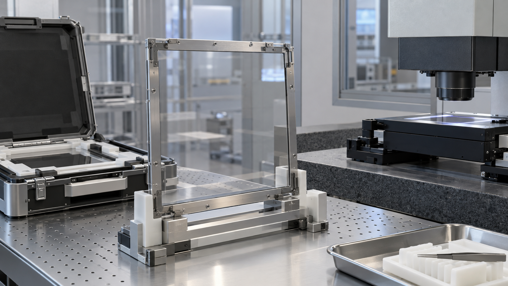
A pellicle is an ultrathin membrane stretched in front of the mask to keep particles off it, since a particle that prints would put the same defect on every wafer. Choi et al. (2024, Nanotechnology) say EUV pellicles are hard to make because they are mechanically fragile at nanometre thicknesses and must withstand the harsh conditions in the tool, including high temperature and hydrogen radicalsSourced. In that paper, metal-silicide membranes were made at the full size of 110 mm × 144 mm and showed over 90% transmittance, under 0.04% reflectance, a 300 µm deflection under a 2 Pa pressure difference and a tensile strength above 2 GPa (aimed at 400 W-class EUV, under the paper's test conditions)Sourced.
Mitsui Chemicals says it produces EUV pellicles under licence from ASML and began commercial production at its Iwakuni-Ohtake Works in 2021Sourced. In its announcement of 28 May 2024 it decided to build production facilities for pellicles with a carbon nanotube (CNT) membrane for High-NA, high-power (600 W or more) EUV, claiming EUV transmittance of 92% or above and light resistance for exposure power over 1 kW (the company's stated values)Sourced. The plan was a capacity of 5,000 sheets per year and a tentative construction end of December 2025Not yet confirmed. We could not confirm the facility's status after the announcement.
With a reflective mask the light passes through the pellicle twice, going in and coming back, so the transmittance counts squared (commentary). At 90% transmittance, 0.9² = 81%; at 92%, 0.92² = about 85%Our calculation. One point of pellicle transmittance accumulates as a loss of light, much like the string of ten mirrors. Assumptions and limits: Choi et al.'s over 90% is a measured value on a prototype membrane in a paper, and Mitsui Chemicals' 92% or above is the company's stated value; their measurement conditions and bases differ, so they are not a ranking.
11. High-NA EUV: NA 0.55, 8 nm
The next step is High-NA EUV, which raises NA from 0.33 to 0.55 (ASML's tool series is called EXE). ASML describes the EXE:5000 as the first 0.55 NA (High NA) EUV system and says the followingSourced.
- Resolution of 8 nm. In a single exposure it prints features 1.7 times smaller than NXE systems, with transistor density 2.9 times higher (manufacturer's stated value)
- 40% more imaging contrast than NXE systems, which ASML says reduces patterned defects and lets chipmakers lower the dose and so raise throughput
- To reach the higher NA it uses new, larger anamorphic optics (mirrors with different reduction in the two directions). That lets chipmakers keep using traditionally sized reticles, but the exposure field is half that of NXE systems, so new, faster wafer and reticle stages are used to maintain productivity
- The design is aimed at "the 2 nm Logic node, followed by Memory nodes at a similar transistor density" (ASML)
Density: if features are 1.7 times smaller, the number per area rises by 1.7² = 2.89, matching ASML's 2.9Our calculation.
Depth of focus (DOF): as a general optical relation, DOF is proportional to λ ÷ NA² (the coefficient depends on conditions; this is our assumption). Going from NA 0.33 to 0.55 at the same wavelength makes it (0.55 ÷ 0.33)² = about 2.8 times shallowerOur calculation.
Assumptions and limits: the DOF coefficient (k2) varies with conditions, and ASML's material does not give the tool's actual DOF. What we show is only a rough measure of the size of the effect of raising NA.
| Item | NXE:3800E (EUV 0.33 NA) | EXE:5000 (High-NA 0.55 NA) |
|---|---|---|
| Wavelength | 13.5 nm | 13.5 nm |
| Projection optics NA | 0.33 | 0.55 |
| Resolution (ASML listing) | 13 nm | 8 nm |
| Throughput (ASML listing) | 220 wafers/h or more (dose 30 mJ/cm²) | 110 wafers/h or more (dose 50 mJ/cm²) |
| Positioning (ASML) | Volume production of 2 nm Logic and leading-edge DRAM nodes | The first High-NA; from the 2 nm Logic node |
All Sourced (ASML product pages [Sources 6, 7], manufacturer's stated values). Because the two tools are listed at different doses, the throughput figures cannot be compared directly.
ASML's 2025 Form 20-F says that the first EXE:5200B, the successor to the EXE:5000, shipped in April 2025, and that at 175 wafers per hour it offers 60% higher productivity than the EXE:5000, thanks to an improved light sourceSourced. It also states that customers had run more than 400,000 wafers on High-NA tools by the end of 2025 and that the EXE:5200B was demonstrated at full specification at a customer siteSourced. ASML expects the EXE platform to start supporting high-volume manufacturing in 2027Not yet confirmed. The dose condition for the 175 wafers per hour is not given in the material we read, so the basis for comparison with the EXE:5000 is unknown.
A shallower DOF means less margin in wafer flatness and in the "in-focus thickness" that includes the resist film. That pushes toward thinner resist films, so materials must absorb enough light and resist etching even when thin (commentary; resist materials are covered in our explainer on resists and photomasks, and etch resistance and underlayers in our explainer on etching). Higher contrast, together with the shadowing caused by the changed angle of incidence on a reflective mask (mask 3D effects), also leads to a rethink of absorber material and thickness (this too belongs to the mask-materials explainer). Tool performance is set by the stacking of all the materials, including resists, masks and pellicles, not by the optics alone. That is the view that runs through this whole series.
12. How to read the numbers: keep stated values, papers and calculations apart
| Number | What it is | Category | Caution |
|---|---|---|---|
| 13 nm / 8 nm | Resolution of the NXE:3800E / EXE:5000 | Manufacturer's stated value | Pattern, illumination and resist conditions are not on the page |
| 38 / 40 nm | NXT:2000i production resolution (dipole / C-quad) | Manufacturer's stated value | Stated with illumination conditions. Not directly comparable with EUV values |
| 220, 110, 175 wafers/h | Throughput of the NXE:3800E, EXE:5000, EXE:5200B | Manufacturer's stated value | Dose conditions differ (30 and 50 mJ/cm² for the first two, unknown for the last) |
| About 5%; over 20 kW → 200 W | Source conversion efficiency; laser power needed | Peer-reviewed paper (2017) | Describes the NXE:3300B generation. A lower-bound guide |
| 1,000 W | Demonstrated EUV source power (April 2025) | Manufacturer's statement (20-F) | A demonstration, not a production specification |
| 70% (13.5 nm, 50 bilayers) | Reflectance of a Mo/Si multilayer | Peer-reviewed paper (2002) | Laboratory sample. Not a production mirror value |
| About 2% | Transmission with 10 reflections at 67% | Peer-reviewed paper (2017) / reproduced by our calculation | The reflection count is an example. Current tools not confirmed |
| Over 90% / 92% or above | EUV pellicle transmittance | Peer-reviewed paper (2024) / manufacturer's stated value (2024) | Measurement conditions and bases differ. Not a ranking |
| 400,000+ wafers; 2027 | Wafers run on High-NA; expected start of volume manufacturing | Manufacturer's statement (20-F) / expectation | 2027 is an expectation: Not yet confirmed |
13. Limits and what we could not confirm
(1) We could not confirm mirror counts in current tools or tool uptime
The number of mirror reflections, tool uptime and effective throughput at customers' fabs do not appear in the published material we read. "Ten mirrors, about 2%" is only an example given in a 2017 paper.
(2) Equipment makers' numbers are stated values
The resolution and throughput on ASML's pages are the manufacturer's stated values. Conditions such as pattern, illumination, resist and tolerated variation are not on the pages. That is why our k1 back-calculation is only a rough guide.
(3) Other approaches, and approaches without light, are not covered
We do not cover EUV sources other than laser-produced plasma, electron-beam writing or nanoimprint. Nanoimprint is covered in our explainer on self-assembly and nanoimprint in this series.
(4) The chemistry of resists, masks, ALD and etching comes in the next three articles
This article only outlines the light-sensitive resist chemistry, mask materials, ALD and etching. Stochastic defects are taken up in our explainer on resists and photomasks.
- The smallest dimension follows CD = k1 × λ ÷ NA. ASML gives the physical limit of k1 as 0.25Sourced
- ArF immersion has NA 1.35 and a stated production resolution of 38 to 40 nm. Back-calculated, k1 is about 0.27 to 0.28, close to the limitOur calculation
- The way past the optical limit is multiple patterning with spacers, which adds deposition and etch work (commentary)
- EUV (13.5 nm) cannot use lenses, so it is a world of mirrors, vacuum and a tin-plasma source. In the ten-reflection example, about 2% of the light reaches the waferSourced
- Photon energy is about 14 times higher and the photon count at the same dose about 14 times lower (about 290 down to about 20 per nm² at an assumed 30 mJ/cm²)Our calculation
- High-NA (0.55) has a stated resolution of 8 nm, and by our calculation the DOF is about 2.8 times shallower. ASML expects it to support volume manufacturing from 2027Not yet confirmed
14. Glossary
- Lithography (exposure)
- The step that transfers an original's pattern onto the resist on a wafer with light.
- CD
- Critical dimension. The smallest dimension that can (or must) be printed.
- NA
- Numerical aperture. A number describing how wide a cone of light the optics can collect.
- k1
- A process-dependent coefficient. Its physical limit is 0.25 (ASML).
- DUV / ArF / KrF
- Deep ultraviolet / the 193 nm laser / the 248 nm laser.
- Immersion
- Putting water between lens and wafer to shorten the effective wavelength and raise NA above 1.
- EUV
- Extreme ultraviolet, 13.5 nm. Lenses cannot be used, so mirrors are.
- LPP
- Laser-produced plasma. Getting light by hitting tin droplets with a laser.
- Intermediate focus (IF)
- The focal point of EUV light at the border between the source and the scanner.
- Reticle / photomask
- The original carrying the circuit pattern. For EUV it is reflective.
- Pellicle
- An ultrathin dust-protection membrane in front of the mask.
- SADP / SAQP
- Self-aligned double / quadruple patterning. Spacers halve / quarter the pitch.
- DOF
- Depth of focus. The range of depth over which the image stays in focus.
- High-NA
- EUV with NA 0.55. ASML's tool series is called EXE.
- OPC
- Optical proximity correction. Computational correction of the original's pattern in advance.
15. References (primary sources)
- ASML "CD = k1 • λ / NA" (the Rayleigh criterion), technical explainer, accessed 9 October 2026 — asml.com
- ASML "Light and lasers", technical explainer, accessed 9 October 2026 — asml.com
- ASML "Lenses & mirrors", technical explainer, accessed 9 October 2026 — asml.com
- ASML "Pushing k1 further", technical explainer, accessed 9 October 2026 — asml.com
- ASML "TWINSCAN NXT:2000i", product page (manufacturer's stated values), accessed 9 October 2026 — asml.com
- ASML "TWINSCAN NXE:3800E", product page (manufacturer's stated values), accessed 9 October 2026 — asml.com
- ASML "TWINSCAN EXE:5000", product page (manufacturer's stated values), accessed 9 October 2026 — asml.com
- ASML Holding N.V. Form 20-F for the year ended 31 December 2025 (Annual Report 2025), filed with the U.S. SEC — sec.gov
- Fomenkov I et al. "Light sources for high-volume manufacturing EUV lithography: technology, performance, and power scaling", Advanced Optical Technologies 6(3-4), 173–186 (2017, peer-reviewed) — doi.org/10.1515/aot-2017-0029
- Bajt S et al. "Improved reflectance and stability of Mo/Si multilayers", Optical Engineering 41(8), 1797–1804 (2002, peer-reviewed) — doi.org/10.1117/1.1489426
- Lin BJ "Immersion lithography and its impact on semiconductor manufacturing", Journal of Micro/Nanopatterning, Materials, and Metrology 3(3), 377–500 (2004, peer-reviewed; the journal's earlier title was JM3) — doi.org/10.1117/1.1756917
- Mitsui Chemicals "Mitsui Chemicals Sets up Production Facilities for CNT Pellicles to Be Used in Next-Gen EUV Lithography", news release, 28 May 2024 — jp.mitsuichemicals.com
- Choi M et al. "Development and optimization of metal silicide EUV pellicle for 400W EUV lithography", Nanotechnology 36(6), 06LT01 (2024, peer-reviewed) — doi.org/10.1088/1361-6528/ad902d
- US patent US 11,676,817 B2 "Method for pitch split patterning using sidewall image transfer" (Tokyo Electron Limited, published 13 June 2023; only the description is cited and its claims are not interpreted) — patents.google.com
- ASML "TWINSCAN NXT:2050i", product page (manufacturer's stated values), accessed 9 October 2026 — asml.com
16. Claim-to-source audit
| Claim in the text | Basis | Label |
|---|---|---|
| The minimum-size equation CD = k1 × λ ÷ NA, the definitions of NA and k1, the physical limit of k1 at 0.25, the three routes to smaller features (wavelength, NA, k1), and that a new wavelength needs new light sources, optical materials and resists | ASML technical explainers (accessed 9 October 2026)[Source 1] https://www.asml.com/en/technology/lithography-principles/rayleigh-criterion [Source 4] https://www.asml.com/en/technology/lithography-principles/pushing-k1-further | Sourced |
| The history of sources (g-line 436 nm, i-line 365 nm, KrF 248 nm, ArF 193 nm, EUV 13.5 nm), EUV being more than 14 times shorter than DUV, tin droplets about 25 µm at 70 m/s and 50,000 per second, a weak pulse to flatten then a strong pulse to vaporize | ASML technical explainer (Light and lasers)[Source 2] https://www.asml.com/en/technology/lithography-principles/light-and-lasers | Sourced |
| No lenses for EUV because most materials absorb it, multilayer mirrors in vacuum, more than 100 layers per mirror, surface smoothness below one atom's thickness. Immersion (2003) giving NA 1.35, DUV optics over 1.2 m tall and over a tonne, the move from 0.33 to 0.55 NA, and EUV printing smaller despite lower NA because of its shorter wavelength | ASML technical explainer (Lenses & mirrors)[Source 3] https://www.asml.com/en/technology/lithography-principles/lenses-and-mirrors | Sourced |
| Illumination tricks (off-axis, pupil shapes, a free-form illuminator) and computational lithography (OPC) to lower k1 | ASML technical explainer (Pushing k1 further)[Source 4] https://www.asml.com/en/technology/lithography-principles/pushing-k1-further | Sourced |
| NXT:2000i: NA 1.35, 193 nm, production resolution 40 nm (C-quad) and 38 nm (dipole), 4× reduction, 26 × 33 mm field, compatible with existing reticles, a champion 4,600 wafers per day (manufacturer's stated values) | ASML product page (manufacturer's stated values)[Source 5] https://www.asml.com/en/products/duv-lithography-systems/twinscan-nxt2000i | Sourced |
| ASML's statement on the NXT:2050i page that a new immersion hood reduces water loss and improves defectivity | ASML product page (manufacturer's stated values)[Source 15] https://www.asml.com/en/products/duv-lithography-systems/twinscan-nxt2050i | Sourced |
| NXE:3800E: wavelength 13.5 nm, resolution 13 nm, NA 0.33, 220 wafers/h or more (dose 30 mJ/cm²), for volume production of 2 nm Logic and leading-edge DRAM nodes | ASML product page (manufacturer's stated values)[Source 6] https://www.asml.com/en/products/euv-lithography-systems/twinscan-nxe-3800e | Sourced |
| EXE:5000: NA 0.55, resolution 8 nm, 110 wafers/h or more (dose 50 mJ/cm²), features 1.7 times smaller and density 2.9 times higher, 40% more imaging contrast than NXE, anamorphic optics, existing reticle size kept, exposure field half that of NXE | ASML product page (manufacturer's stated values)[Source 7] https://www.asml.com/en/products/euv-lithography-systems/twinscan-exe-5000 | Sourced |
| EXE:5200B first shipped April 2025, 175 wafers/h and 60% more productive than EXE:5000, full specification demonstrated at a customer, more than 400,000 wafers run on High-NA by end of 2025, NXE:3800E shipped at full specification of 220 wafers/h, a 1,000 W source demonstrated in April 2025, ASML being the only EUV tool maker, and the shift from multi-patterning to single patterning (fewer masks and steps) | ASML Form 20-F (fiscal 2025)[Source 8] https://www.sec.gov/Archives/edgar/data/0000937966/000162828026011378/asml-20251231.htm | Sourced |
| That the EXE platform is expected to start supporting volume manufacturing in 2027, and the adoption of the 1,000 W source as a production specification | ASML 20-F statement of expectation. The 1,000 W is a demonstration; the material gives no timing for production specification[Source 8] https://www.sec.gov/Archives/edgar/data/0000937966/000162828026011378/asml-20251231.htm | Not yet confirmed |
| Source conversion efficiency about 5%, more than 20 kW of laser for 200 W at the intermediate focus, more than 200 W for 100 wafers/h (60% duty cycle), ArF sources at 90 W for 200 wafers/h, the spectrum at 13.5 nm within 2% bandwidth, 10 reflections at 67% peak reflectivity giving about 2% transmission, collector lifetime as a top challenge, hydrogen buffer gas and protective layers | Fomenkov et al. (2017, peer-reviewed; a description of the NXE:3300B generation)[Source 9] https://doi.org/10.1515/aot-2017-0029 | Sourced |
| Mo/Si multilayer (50 bilayers, B4C of 0.25 to 0.4 nm at the interfaces) with 70% reflectance at 13.5 nm and normal incidence (0.545 nm bandwidth), bilayer contraction reduced by about 30%, Ru termination greatly improving oxidation resistance (laboratory samples) | Bajt et al. (2002, peer-reviewed)[Source 10] https://doi.org/10.1117/1.1489426 | Sourced |
| Water immersion effectively shortening 193 nm to 135 nm | Lin (2004, peer-reviewed abstract)[Source 11] https://doi.org/10.1117/1.1756917 | Sourced |
| That Mitsui Chemicals produces EUV pellicles under ASML licence and began commercial production in 2021, decided on 28 May 2024 to build CNT pellicle production facilities, 92% or above transmittance and light resistance for over 1 kW (company's stated values), 5,000 sheets per year, tentative end of construction December 2025 | Mitsui Chemicals news release (28 May 2024). The facility plan is as of the announcement[Source 12] https://jp.mitsuichemicals.com/en/release/2024/2024_0528_1/index.htm | Not yet confirmed |
| That EUV pellicles are mechanically fragile and must withstand high temperature and hydrogen radicals; metal-silicide membranes made at full size of 110 × 144 mm with over 90% transmittance, under 0.04% reflectance, 300 µm deflection at 2 Pa and tensile strength above 2 GPa | Choi et al. (2024, peer-reviewed)[Source 13] https://doi.org/10.1088/1361-6528/ad902d | Sourced |
| That in SADP spacers are formed around mandrels and the mandrels removed to give a pattern at half the minimum pitch of the lithography system (one quarter for SAQP), that 193 nm immersion was extended to pitches below 30 nm, and that SIT arose from overlay-error concerns in two-exposure schemes | Background and embodiment description of US 11,676,817 B2 (claims not interpreted)[Source 14] https://patents.google.com/patent/US11676817B2/en | Sourced |
| The k1 back-calculation (38 × 1.35 ÷ 193 = 0.266; 0.280 for 40 nm; 13 × 0.33 ÷ 13.5 = 0.318; 8 × 0.55 ÷ 13.5 = 0.326), and that it is only a guide because the definition of the minimum size is unknown | Our calculation. λ, NA and minimum sizes are the manufacturer's stated values on ASML product pages; k1 is not a published value | Our calculation |
| 193 ÷ 13.5 = about 14.3, 193 ÷ 135 = about 1.43 (corresponding to water's refractive index), 1.7² = 2.89 (density), (0.55 ÷ 0.33)² = about 2.8 (relative change in DOF, assuming the general relation DOF proportional to λ ÷ NA²) | Our calculation. The DOF coefficient depends on conditions and is assumed | Our calculation |
| 200 W ÷ 20 kW = about 1%, 20 kW × 5% = 1 kW, 200 W ÷ 1 kW = about 20% (share left after collection and gas transmission) | Our calculation. Based on the figures of Fomenkov et al. [Source 9]; 20 kW is a lower-bound guide | Our calculation |
| Transmission = R to the n: 0.67 to the 10 = about 1.8%, 0.70 to the 10 = about 2.8%, and the values for n = 2 to 10 in Fig. 6. A pellicle is passed twice, so 0.9² = 81% and 0.92² = about 85% | Our calculation. Ten reflections is an example; it does not consider current tools or whether the reticle reflection is counted | Our calculation |
| Photon energy (1239.84 eV·nm ÷ wavelength) of about 6.4 eV at 193 nm and about 92 eV at 13.5 nm; incident photons at 30 mJ/cm² of about 290 per nm² for ArF and about 20 for EUV, about 2,000 in 10 nm × 10 nm, and about 2% shot noise (1 ÷ √N) | Our calculation. 30 mJ/cm² is the condition for the throughput on ASML's tool page [Source 6], not a real resist dose | Our calculation |
| The need for water-repellent surfaces or topcoats on immersion resists, the shared logic of interface design and deposition in multilayers, the effect of reduced focus depth at higher NA on resist thickness margin, multiple patterning adding deposition and etch work, and each materials-engineer box | This article's organization and commentary based on the published content. Specific materials and specifications were not confirmed | Commentary |
| Mirror reflection counts in current tools, tool uptime, effective throughput at customers' fabs, the dose condition of the EXE:5200B, and the operating status of the CNT pellicle facility | Could not be confirmed from primary sources within the scope of this article, so not stated | Commentary |
| That Figs. 2 to 7 are explanatory drawings, not real design or measurement drawings, and that Figs. 1 and 8 are AI-generated images | This article's note | Commentary |
Last updated: 9 October 2026 / Sources are limited to primary material (official documents and SEC filings of equipment makers, peer-reviewed papers, patent publications and company announcements). Because structural readings and materials-design interpretations are included, they are marked as "Commentary" and kept apart from sourced facts. Mirror reflection counts in current tools, tool uptime, effective throughput at customers' fabs and how High-NA is used in volume production could not be confirmed, so they are not stated. All equipment makers' numbers are the manufacturers' stated values; values stated under different conditions are not placed side by side to rank them. The figures are explanatory diagrams. Figs. 2 to 7 are vector drawings and Figs. 1 and 8 are AI-generated images; none of them shows an actual photograph or design of a tool, mask or pellicle.