TECHNOLOGY EXPLAINER
Nanoscale Memory
— NAND that went up when it could no longer shrink sideways, and new memories that fall short of “replacement”
Semiconductor memory now advances by stacking more than by shrinking. NAND flash has moved to a three-dimensional structure of more than 300 layers; DRAM is nearing the limit of shrinking its one transistor and one capacitor; and new memories such as MRAM, ReRAM and phase-change memory (PCM) have two faces: in volume production as embedded memory, struggling as large standalone parts. This explainer draws on the IRDS roadmap, official material from Kioxia, TSMC and Everspin, and conference papers to lay out the 3D structure of NAND, the scaling limits of DRAM, the principles and status of new memories, and the materials issues. Company plans are labelled as plans, and laboratory demonstrations are never presented as the performance of production parts.
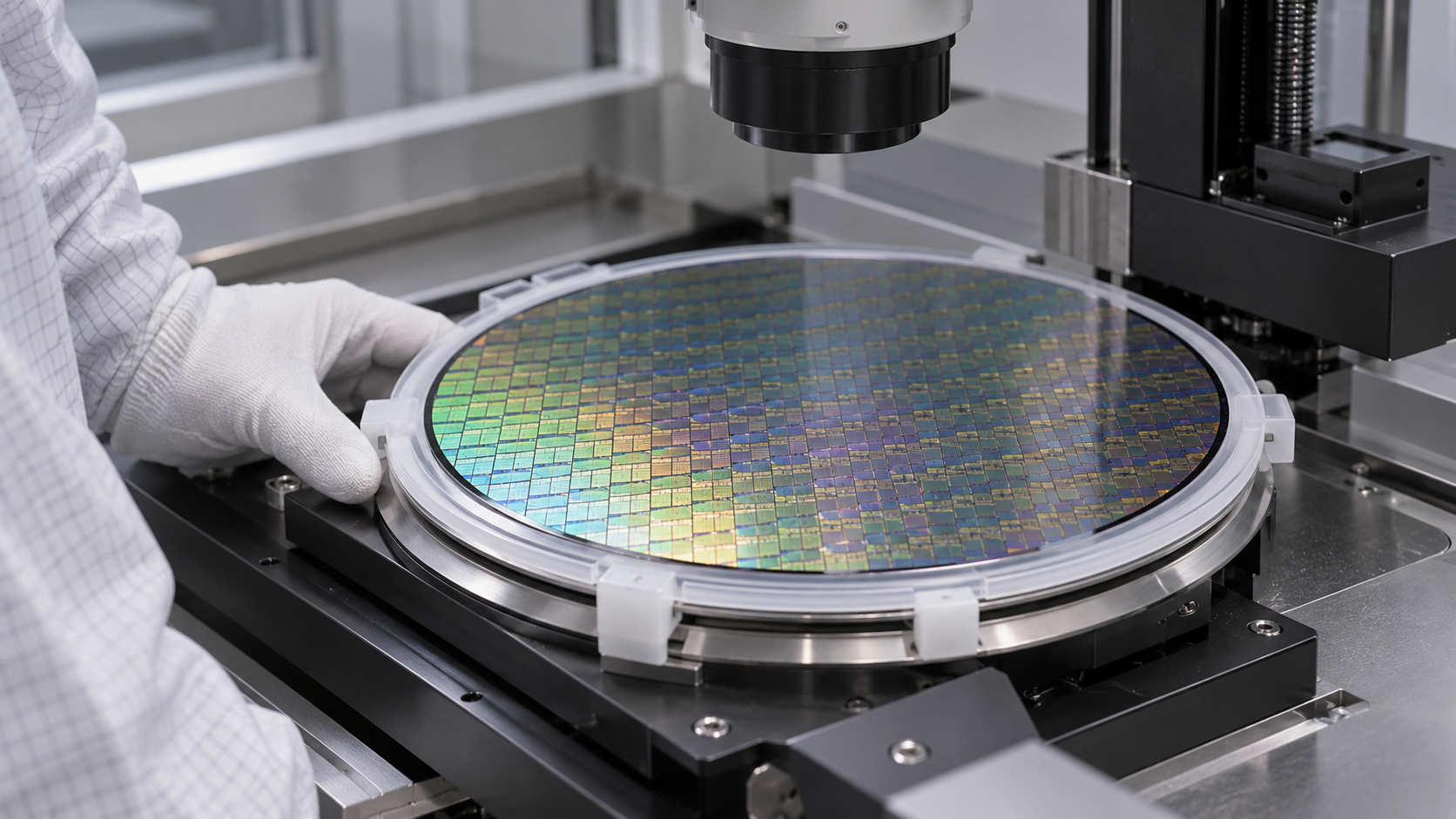
- Three kinds of memory: NAND, DRAM and new memories
- NAND: why stack vertically
- Our calculation: the height of 332 layers and the footprint of one string
- A materials engineer's view (1): the more you stack, the harder the materials for holes, channels and wiring
- DRAM: the limit of shrinking 1T1C
- New memories (MRAM, ReRAM, PCM, ferroelectric): principles and status
- Embedded versus standalone: use decides the fate
- A materials engineer's view (2): the tug-of-war between retention and writing in the MTJ
- What is still hard, and what could not be confirmed
- Glossary / References / Claim-to-source audit
Sourced = stated in published material (link given)
Our calculation = a figure this article derived, with the assumptions spelled out
Not yet confirmed = a plan, target or projection by a company or institution with no confirmed result or volume start
Structural readings and materials-design interpretations are marked separately as Commentary, and weakly supported ideas as Inference.
Kioxia's technical topics introduce research presentations and are not specifications of production products. Single-device or prototype values from the laboratory are not presented as the performance of production parts.
1. Three kinds of memory: NAND, DRAM and new memories
IRDS 2023 treats memory as DRAM and non-volatile memory (NVM), with standalone chips driving the technology and embedded memory following the same trends with some lag Sourced.
- NAND flash: one transistor serves as both storage and selection. According to IRDS, flash currently serves more than 99% of non-volatile memory applications. Planar (2D) NAND hit the limit of how few electrons it could store and was replaced by 3D NAND stacked vertically Sourced
- DRAM: one transistor (T) and one capacitor (C) store one bit (1T1C). The goal is to shrink the cell area to 4F² (F is the minimum feature size). Keeping capacitance up while holding leakage down is the challenge Sourced
- New memories: they store data not as charge but as magnetization (MRAM), resistance (ReRAM), crystalline or amorphous phase (PCM), or ferroelectric polarization (FeRAM, FeFET). IRDS calls these “emerging” memories Sourced
2. NAND: why stack vertically
IRDS explains that when the number of stored electrons in a 2D NAND cell reaches statistical limits, the threshold-voltage distribution becomes uncontrollable and logic states unpredictable, so the density of charge-based devices cannot rise indefinitely Sourced. Density therefore rises by stacking memory layers. Stacking finished devices one layer at a time is of doubtful economy, because the cost per bit starts to rise after a few layers. The roadmap says a turning point was the “punch and plug” approach proposed in 2007 Sourced. It turns the NAND string (the column of cells along the bit line) by 90 degrees from horizontal to vertical, leaving the word lines as horizontal planes; it was named BiCS (Bit Cost Scalable). The original paper is Tanaka et al., “Bit Cost Scalable Technology with Punch and Plug Process for Ultra High Density Flash Memory” (VLSI 2007) [Reference 22; only title and bibliographic details checked].
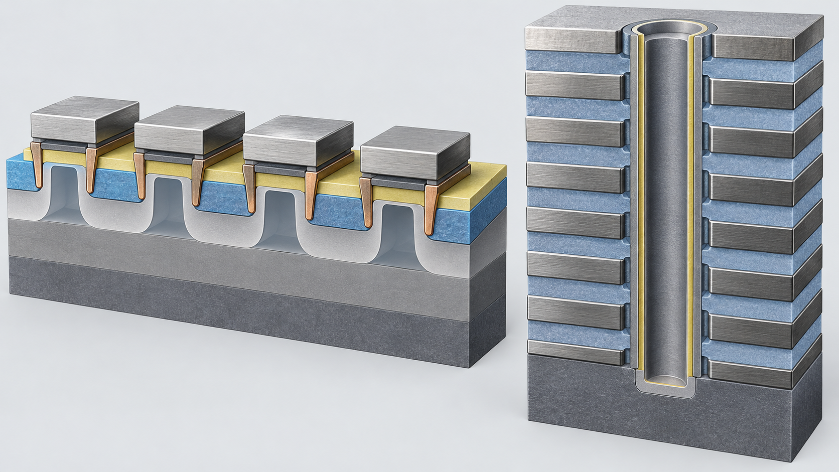
Shapes, colors and dimensions are illustrative. Consult the original schematic below for exact values and label correspondence.
View the original SVG schematic and exact annotations
Reading guide and original schematic labels: NAND went from "side by side" to "stacked vertically" (conceptual diagram) / Schematic cross-sections; not real layer counts, dimensions or film thicknesses. / Two-dimensional (planar) NAND / Three-dimensional NAND (BiCS type) / Cells side by side (fewer electrons as it shrinks) / IRDS: electron count nears a statistical limit / Word lines (orange) stacked flat; channel (blue) in vertical holes / More layers give more density / The limit of 2D NAND and the BiCS idea follow IRDS 2023 [Ref. 1]; the original proposal is Tanaka et al. (VLSI 2007) [Ref. 22]. / Layer counts and hole counts are simplified; not the structure of any real product.
IRDS 2023 notes that the x-y dimensions of 3D NAND (equivalent to cell size in 2D) are about 100 nm and higher, far larger than the roughly 15 nm of the smallest 2D NAND, and that the difference is made up by stacking many layers Sourced. It also says products with more than 250 layers are in volume production and that some see 500+ layers, even 1000 layers, as possible. On bits per cell, 4 bits (QLC) are in volume production, and 5 bits or more are expected to become viable before long; more bits per cell trade off performance, since programming and reading take longer and reliability suffers, in exchange for lower cost Sourced.
| What was published | Source and level |
|---|---|
| BiCS FLASH 10th generation: 1 Tb, 3 bits per cell (TLC), 332 word-line layers, areal density 29 Gb/mm² (which the company describes as the world's highest for a 1 Tb product), data rate 4.8 Gbps. Developed jointly by Kioxia and Sandisk. CBA (CMOS directly Bonded to Array) structure | Kioxia advanced-technology topic (posted 18 June 2025), introducing the presentation at ISSCC 2025 [Reference 2]. An introduction to a research presentation, not a shipping specification |
| BiCS FLASH 10th generation: 2 Tb, 4 bits per cell (QLC), areal density 37.6 Gb/mm², write throughput above 85 MB/s, six-plane architecture. The layer count follows the TLC product | Kioxia advanced-technology topic (posted 15 July 2026), introducing the presentation at ISSCC 2026 [Reference 3]. Same level |
| CBA structure: CMOS peripheral circuits and the cell array are made on separate wafers and joined through Cu bonding pads. It removes the high-aspect-ratio contacts that the earlier CUA (CMOS Under Array) needed, and lets the best process temperature be used for each of CMOS and the array | Kioxia advanced-technology topic (posted 14 March 2024). Applied to the 8th generation of BiCS FLASH [Reference 4] |
All Sourced. “World's highest” and similar phrases are Kioxia's own statements (company claims). Layer counts and densities of other makers' NAND are not covered because no primary source was used for them here (no ranking is made).
3. Our calculation: the height of 332 layers and the footprint of one string
From the published layer count and density, we estimate the order of magnitude of 3D NAND's “height” and “footprint” Our calculation.
- Stack height: IRDS says that 200 layers, at about 50 nm per layer, give a stack about 10 µm tall Sourced. Extending to 332 layers: 332 × 50 nm = about 16.6 µm. At 25 nm per layer it would be about 8.3 µm (the per-layer thickness is our assumption; real product values could not be confirmed)
- Hole aspect ratio: taking a hole diameter of 100 nm (the level of IRDS's x-y dimension; our assumption), depth / diameter = 8.3 to 16.6 µm / 0.1 µm = about 83 to 166
- Footprint of one string: 29 Gb/mm² ÷ 3 bits ÷ 332 layers = about 2.9×10⁷ strings/mm². Area per string = 1012 nm² ÷ 2.9×107 = about 34,000 nm², that is, a square about 185 nm on a side (about 179 nm if Gb means 230)
- The same for the QLC product: 37.6 Gb/mm² ÷ 4 bits ÷ 332 layers = about 2.8×10⁷ strings/mm², a square about 188 nm on a side
- A guide to the chip area holding 1 Tb: 1,024 Gb ÷ 29 Gb/mm² = about 35 mm²
Assumptions and limits: this uses the area of the whole chip (including peripheral circuits and bonding pads), so the real footprint of the cell array alone should be smaller. It takes 332 word-line layers and 3 or 4 bits, and ignores redundant and dummy cells. All are estimates from our assumptions and not the dimensions of any real product. The point is the order of magnitude: one string has a footprint under 200 nm, larger than a 2D NAND cell (about 15 nm) but with more than 300 cells stacked inside it.
4. A materials engineer's view (1): the more you stack, the harder the materials for holes, channels and wiring
All four points below are based on Kioxia's introductions to research presentations. We did not confirm whether they are applied to production products, except where stated.
- 1. Etching the memory hole: the memory hole needs a cylindrical shape with little device-to-device variation, yet bowing, striation, taper, hole distortion and twisting and other shape anomalies arise, Kioxia reports Sourced [Reference 5]. Its model of striation is that a rough surface forms on the fluorocarbon film deposited on the hole sidewall and is transferred with enlargement of the hole diameter. On throughput, deeper holes take longer to etch, so it widened the candidate gases, chose C3HF5, and applied it to volume production of BiCS FLASH 8th generation. A 5.6 µm full-etch result and a global warming potential (GWP) below 1 for this gas are also reported Sourced [Reference 6]
- 2. Silicon for the channel: with more layers the poly-Si channel gets longer, resistance rises and cell current runs short. Metal-induced lateral crystallization (MILC) is being developed to fix this: NiSi2 grains diffuse through amorphous Si and leave crystalline Si behind. First-principles calculations identified the rate-limiting step as diffusion of Ni vacancies through NiSi2, and suggested tensile stress lowers the diffusion energy Sourced [Reference 8]. A 2020 report said that threshold variation arising from poly-Si grain boundaries was the issue, and that MILC-crystallized channels gave better electrical characteristics and smaller variation than poly-Si Sourced [Reference 9]
- 3. The word-line metal: shrinking the word-line pitch raises resistance and RC delay, and scaling in XY along with it degrades tungsten (W) gap fill. Voids left by poor fill hold residual fluorine from the WF6 precursor, which etches the insulators and causes leakage failures, it is reported. Molybdenum (Mo) was examined as a remedy. Mo has lower resistivity than W and its precursor MoO2Cl2 contains no fluorine. The report gives a leakage-failure rate for Mo word lines one-hundredth that of W, an 18% RC improvement when the word-line pitch is shrunk 17%, and a bit-density gain of 16.3% or more in the same silicon volume. Even with Mo, however, poor fill leaves residual oxygen in voids and raises leakage failures Sourced [Reference 10]
- 4. Charge-storage layer, interface and rethinking structure: as layers increase, the supply of holes needed for erase may fall short, and a structure with a Schottky source junction, made by depositing a metal at the end of the channel, has been proposed [Reference 11]. As a future generation, a Horizontal Channel Flash that lays the channel horizontally (so cell current does not fall with layer count) has been proposed, and a structure that puts an ultra-thin Mo film of about 0.1 nm between the Si floating gate and the insulator to improve programming was presented at a conference in May 2026. In high-aspect-ratio memory holes, Mo deposited by ALD showed a sidewall-to-top thickness ratio (coverage) of 90% or more, better than TiN Sourced [References 12, 13]
What a materials engineer can read from this is that stacking makes three kinds of “depth” problems harder at once: the deep hole, the long channel and the metal that must fill narrow gaps (our commentary). Atomic layer deposition and etching are covered in the series explainers on atomic layer deposition and on etching.
5. DRAM: the limit of shrinking 1T1C
IRDS 2023 states the main goal for DRAM as shrinking the 1T1C cell down to 4F², regarded as the practical limit. The most common cell today is 6F² (a cell area six times the square of the minimum feature size F) Sourced. The challenges are vertical transistors and high-k dielectrics that raise capacitance density while holding leakage down. As the storage capacitor gets physically smaller, the equivalent oxide thickness (EOT) must be cut sharply to keep capacitance. For DRAM with half-pitch between 48 and 30 nm, MIM capacitors use the high-k stack ZrO2/Al2O3/ZrO2; the roadmap says this material evolution continues to the 20 nm generation, after which ultra-high-k materials (perovskites with a relative permittivity of 50 to 100) will be needed Sourced. The 3D shape of the capacitor is expected to change from cylinder to pillar.
Another constraint is that cell processes come after the peripheral CMOS has been formed, so they are limited to low-temperature processing. The roadmap adds that if DRAM scaling loses efficiency, 3D cell stacking or a new DRAM concept will be needed, but there is no clear path beyond 2D DRAM Sourced. The challenges of etching high-aspect-ratio contacts for DRAM capacitor formation are treated in the SPIE paper by Kim et al. (2015) [Reference 25; only title and bibliographic details checked].
What happens to the cell area in going from 6F² to 4F², under assumptions we set Our calculation.
- Assumption: F = 20 nm (an example at the generation level IRDS mentions; not a real product's value)
- 6F²: 6 × 20 × 20 = 2,400 nm²
- 4F²: 4 × 20 × 20 = 1,600 nm² (two-thirds of 6F², a 33% reduction)
- Cells in the same area: 6 ÷ 4 = 1.5 times
Assumptions and limits: F is an assumption. Shrinking the cell area does not relax the need to keep capacitor capacitance, so the capacitor has to be made taller (thinner and deeper) to make up for the lost area. Real capacitor dimensions and capacitance could not be confirmed in the official material used here.
| What was published (research stage) | Source and level |
|---|---|
| OCTRAM: a 4F² DRAM whose cell transistor is a vertical GAA transistor of the oxide semiconductor InGaZnO. On-current 15 µA, off-leakage 10−18 A (1 aA). Prototyped with Nanya Technology, with retention above 100 seconds confirmed. A “capacitor-first” structure puts the cell transistor on top of the capacitor | Kioxia advanced-technology topic (posted 13 February 2025) [Reference 14]. A prototype research presentation, not a production product |
| OCTRAM transistors face shortened time-dependent dielectric breakdown (TDDB) lifetime as they shrink; the report finds intrinsic degradation from scaling and extrinsic degradation from transistor shape and process damage | Kioxia advanced-technology topic (posted 18 September 2025) [Reference 15]. Same level |
| 3D-DRAM: a folded capacitor claimed to give more than 3.3 times the storage capacitance and a 28% better bit-cell density in the same footprint than a 3D-DRAM with a horizontal capacitor. Evaluated with TCAD simulation and a compact model | Kim et al., IEEE Electron Device Letters (October 2026) [Reference 26]. A proposal based on simulation, not a prototype |
All Sourced. All are research-stage reports and do not indicate timing or plans for volume production Not yet confirmed.
6. New memories (MRAM, ReRAM, PCM, ferroelectric): principles and status
IRDS notes that emerging memories are two-terminal structures (a resistor or a capacitor), so a separate selection element has to be combined with them (1T-1C, 1T-1R, 1D-1R and so on) Sourced. The table below arranges principle, materials and status from IRDS 2023 and the companies' official pages.
| Type | How it stores data, and materials | Status confirmed in official material |
|---|---|---|
| MRAM (magnetic) | Magnetic tunnel junction (MTJ): two ferromagnetic layers separated by a thin insulating tunnel barrier; resistance changes depending on whether the magnetizations are parallel or opposed. Spin-transfer torque (STT) switches the magnetization. Scaling calls for perpendicular magnetization materials (IRDS). Kioxia's reports concern CoFeB/MgO-type junctions | Embedded: TSMC states that its 22 nm and 16 nm eMRAM have passed automotive AEC-Q100 qualification and are in production, with 12 nm (automotive-grade) and 5 nm under development [Reference 20]. Standalone: Everspin sells discrete STT-MRAM (its page lists parts such as 4 Mb xSPI devices, and describes STT-DDR for data centers) [Reference 21]. IRDS says the hope of STT-MRAM replacing NAND seems remote, and treats it mainly as embedded memory |
| ReRAM (resistive) | Resistance change in a metal-insulator-metal (MIM) structure. A filament made of only a few atoms (ions) changes the resistance (IRDS) | Embedded: TSMC states eRRAM is in volume production at 40, 28, 22 and 12 nm (the second-generation 22 nm is automotive-qualified; the third-generation N12e is in volume production), with 6 nm under development [Reference 20]. Large standalone: IRDS 2023 stopped tracking high-density ReRAM (difficulty of meeting reliability requirements for large arrays; statistical fluctuation of the filament) |
| PCM (phase-change) | The resistance difference between the crystalline and amorphous states of a chalcogenide (typically Ge2Sb2Te5, GST). RESET melts and quenches with a short electric pulse into the amorphous state; SET crystallizes with a longer pulse (usually over 100 ns) (IRDS). For a review see Raoux et al. 2008 [Reference 23; only title and bibliographic details checked] | IRDS: used since 2011 to replace NOR in feature phones and in volume production at about 45 nm since 2012, but no new product since. 3D XPoint (cross-point) was withdrawn from the market within the past two years and is currently unavailable (the reason was not announced; the lack of a common interface and the narrowing of its cost gap over DRAM are suggested as partial causes) |
| FeRAM / FeFET (ferroelectric) | Data stored in the polarization of a ferroelectric. FeRAM has destructive readout (it must be rewritten after reading, as with DRAM). A ferroelectric FET (FeFET) using HfO2 has been proposed | IRDS: FeRAM is fast, low-power and low-voltage and suited to embedded uses such as RFID and smart cards, but the ferroelectric materials are foreign to CMOS processing and degrade easily. The ferroelectricity of HfO2 was reported by Böscke et al. (IEDM 2011) [Reference 24; only title and bibliographic details checked] |
All Sourced (IRDS 2023 [Reference 1], TSMC [Reference 20], Everspin [Reference 21]). A company's “in production” or “under development” is the company's statement; scale and customers could not be confirmed.
7. Embedded versus standalone: use decides the fate
IRDS says that, for MRAM, its SRAM-like performance and much smaller footprint than a conventional 6T-SRAM have drawn interest in applications that do not need high write endurance, such as mobile devices, so STT-MRAM is generally considered embedded memory rather than standalone Sourced. There is also interest in replacing embedded NOR flash, but for embedded uses needing higher density NOR flash is expected to stay more cost-effective. IRDS also points out that flash keeps its preloaded code through board soldering (about 250°C), whereas many emerging memories have yet to demonstrate solder-reflow tolerance Sourced. TSMC lists for its eMRAM ultra-high-speed read and write, high endurance, solder-reflow support and excellent high-temperature data retention Sourced (company claims).
- In embedded use the target is small SRAM or eFlash, with capacity needs from a few to a few hundred megabits. The decisive factor is whether it can be built from materials and at temperatures that fit the CMOS back end (our commentary)
- As standalone memory the rivals are NAND and DRAM, which keep stacking. IRDS says the success of 3D NAND raised the entry barrier for new memories. On ReRAM it points to reliability in large arrays, and says the original argument that ReRAM, being made of thousands of atoms, is free of statistical fluctuation has become doubtful because the filament is made of only a few atoms (ions) Sourced
- The withdrawal of 3D XPoint is not explained by technical merit alone: IRDS says the reason was not announced, but that the lack of a common interface and the narrowing cost gap from DRAM scaling may be part of it Sourced. It reads as an example of “the materials and principle can work, and the market and standards still stop it” (our commentary)
8. A materials engineer's view (2): the tug-of-war between retention and writing in the MTJ
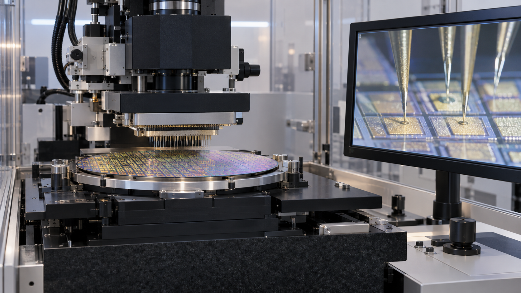
Kioxia says that when the STT-MRAM MTJ is shrunk, the conventional single-layer CoFeB storage layer loses its ability to retain information at diameters of about 20 nm and below Sourced. Its IEDM 2023 report proposes the AccelHR-MTJ, which combines several magnetic layers (a high-retention layer, a layer that accelerates switching, and a spacer layer that exchange-couples them), builds a 14 nm diameter device, and shows retention equivalent to more than 10 years at 90°C together with fast spin-transfer switching with a 5 ns write pulse Sourced [Reference 17; a laboratory demonstration].
How much thermal stability (Δ) does “10-year retention” require, and how does Δ change if the diameter shrinks? An estimate with our assumptions Our calculation.
- Relation: retention time t ≈ τ0 × exp(Δ) (Δ: thermal stability factor = energy barrier / thermal energy). Assumption: attempt time τ0 = 1 ns (our assumption)
- Retention for 10 years (3.156×10⁸ s): Δ = ln(3.156×10⁸ / 10−9) = ln(3.156×10¹⁷) = about 40 (a guide per bit; a large array needs a larger Δ to keep the failure rate down)
- Shrinking the diameter from 20 nm to 14 nm: the area is (14 / 20)² = 0.49. If the storage-layer thickness and anisotropy energy density are the same, Δ also falls to about half (Δ is proportional to volume)
Assumptions and limits: τ0 is an assumption, and holding thickness and anisotropy constant is a simplification. Real MTJ retention is set by the failure-rate requirement per bit and across the array, and by temperature. The point is that Δ falls in proportion to area as diameter shrinks, so materials must raise the perpendicular magnetic anisotropy (PMA) or gain volume by stacking magnetic layers. Kioxia's AccelHR-MTJ reads as an example of the latter (our commentary).
- MRAM: the MTJ is a stack with a tunnel barrier a few nanometers thick (MgO-type). Kioxia observed that applying voltage to a shrunken device for a long time raises resistance and lowers the TMR ratio in a few failing devices. Kioxia and Mie University showed this can be reproduced by generation of oxygen-related defects at the barrier interface, and proposed reducing the initial oxygen vacancies Sourced [Reference 18]. For a larger capacity, a 64 Gb MRAM chip uses a 1S1M structure (selector in series with the MTJ, 4F²) and suppresses read disturb, where reading shares the write path, with a time-controlled discharge readout, showing read reliability with a failure rate of 10 ppm or below (4σ or better) Sourced [Reference 16; research stage]
- ReRAM: the filament being a few atoms makes fluctuation and reliability the issue (IRDS)
- PCM: the large RESET current (IRDS puts it at a fraction of a milliampere), data retention at solder-reflow temperature (about 250°C), and endurance affected by the interaction of phase-change material and electrodes are named as challenges. Kioxia reports a PCM/selector cell with a high-melting Te-rich upper layer and a thin top electrode that promotes heat dissipation, writing three resistance states with a single pulse and keeping the three states after 107 rewrites Sourced [Reference 19; research stage]
- FeRAM and FeFET: ferroelectric materials are ill-suited to CMOS processing and degrade easily (IRDS). HfO2 being close to CMOS materials is cited as the motivation for proposals, but we could not confirm a production product in the official material used here
9. What is still hard, and what could not be confirmed
(1) The limit of stacking NAND
IRDS sees no hard physical limit on stacking, but names possible “etch-stop” effects near an aspect ratio around 100:1 (the roadmap phrases it as a question), where ions are bent by electrostatic charge on the sidewall and can no longer travel down; wafer bowing from stress; and more area for contacts to the word lines. It also says the cost benefit per added layer will eventually diminish Sourced. We could not confirm other makers' latest layer counts or the real dimensions and aspect ratios of memory holes from primary sources.
(2) Kioxia's technical topics are research presentations
Descriptions of Mo word lines, MILC channels, Horizontal Channel Flash, OCTRAM, the 64 Gb MRAM and so on are introductions to conference presentations. Except for items stated explicitly, such as the CBA and C3HF5 gas for BiCS FLASH 8th generation, we did not confirm application to production products.
(3) What comes after today's DRAM
IRDS says 3D cell stacking and new DRAM concepts are discussed, but there is no clear path beyond 2D DRAM Sourced. The OCTRAM and 3D-DRAM proposals are at the research stage. We did not confirm the current generation's dimensions and volume status for each DRAM maker.
(4) Standalone adoption of new memories
Everspin's standalone STT-MRAM is a product, but the densities we could confirm on its page, such as 4 Mb parts, are not at a scale that replaces large NAND or DRAM. IRDS stopped tracking high-density ReRAM, and 3D XPoint PCM was withdrawn.
(5) Company plans
TSMC's 12 nm (automotive) and 5 nm eMRAM and 6 nm eRRAM are under development and are not results Not yet confirmed.
- NAND went vertical: 2D NAND reached its electron-count limit; since BiCS in 2007, products of more than 250 layers are in volume production. The 10th generation has 332 layers and 29 Gb/mm² (a research presentation) Sourced
- A footprint under 200 nm and a depth of a dozen micrometers: from 29 Gb/mm², 3 bits and 332 layers, one string is about 185 nm on a side (an estimate) Our calculation
- The materials issues gather in three kinds of “depth”: etching deep holes, crystallizing long channels, and filling narrow gaps with metal (the W to Mo question) Sourced
- DRAM aims from 6F² to 4F²: two-thirds of the area (assuming F = 20 nm), but there is no clear path beyond 2D Our calculation Sourced
- New memories are in volume as embedded memory and limited as standalone: TSMC's eMRAM (22 and 16 nm) and eRRAM (40 to 12 nm) are in production, IRDS stopped tracking high-density ReRAM, and 3D XPoint was withdrawn Sourced
- Retention falls as the MTJ shrinks: from 20 to 14 nm Δ roughly halves (an assumption); stacked magnetic layers are explored to get both (a laboratory demonstration) Our calculation
10. Glossary
- NAND flash
- Non-volatile memory that stores by presence or absence of charge. One transistor serves as both storage and selection.
- 3D NAND (BiCS)
- A structure with strings standing vertically and word lines stacked as horizontal planes.
- Memory hole
- The thin, deep vertical hole cut through the stacked films of 3D NAND, in which the channel and charge-storage layer are built.
- CBA
- CMOS directly Bonded to Array: peripheral circuits and the cell array made on separate wafers and bonded.
- TLC, QLC
- Schemes that store 3 bits or 4 bits in a cell.
- MILC
- Metal-induced lateral crystallization: crystallizing amorphous Si using nickel silicide.
- DRAM (1T1C)
- Volatile memory that stores one bit with one transistor and one capacitor.
- F, 6F², 4F²
- Cell area expressed as a multiple of the square of the minimum feature size F. 4F² is regarded as the practical limit.
- EOT
- Equivalent oxide thickness: a dielectric's thickness expressed as the SiO2 thickness with the same capacitance.
- MRAM, MTJ
- Magnetic memory, which uses the resistance difference between magnetization states of a magnetic tunnel junction.
- STT
- Spin-transfer torque: switching magnetization with a current.
- ReRAM
- Resistive memory, which uses the resistance change of a metal/insulator/metal structure.
- PCM
- Phase-change memory, which uses the resistance difference between crystalline and amorphous states; chalcogenides such as GST are used.
- FeRAM, FeFET
- A memory that stores by ferroelectric polarization, and a transistor that uses it in the gate.
- Embedded memory
- Memory placed on the same chip as logic and similar; distinguished from standalone memory.
11. References (primary sources)
- IEEE IRDS, "International Roadmap for Devices and Systems 2023: More Moore" (PDF; sections on DRAM, NAND and emerging memory) — irds.ieee.org
- Kioxia advanced-technology topic, "Design and development of the 1Tb 3bit/cell BiCS FLASH 10th generation product" (in Japanese), 18 June 2025 — kioxia.com
- Kioxia advanced-technology topic, "Design and development of the 2Tb 4bit/cell BiCS FLASH 10th generation product" (in Japanese), 15 July 2026 — kioxia.com
- Kioxia advanced-technology topic, "Development of CMOS directly Bonded to Array (CBA) technology for 3D flash memory" (in Japanese), 14 March 2024 — kioxia.com
- Kioxia advanced-technology topic, "Controlling memory-hole etch profiles based on mechanism elucidation" (in Japanese), 28 March 2022 — kioxia.com
- Kioxia advanced-technology topic, "Memory-hole etching with the new C3HF5 gas for higher productivity" (in Japanese), 22 February 2024 — kioxia.com
- Kioxia advanced-technology topic, "Feasibility of measuring high-aspect-ratio profiles of 3D flash memory by T-SAXS simulation" (in Japanese), 28 March 2022 — kioxia.com
- Kioxia advanced-technology topic, "Elucidating the metal-assisted crystallization mechanism for 3D flash memory channels" (in Japanese), 17 December 2024 — kioxia.com
- Kioxia advanced-technology topic, "Development of a single-crystal silicon channel process for 3D flash memory" (in Japanese), 6 March 2020 — kioxia.com
- Kioxia advanced-technology topic, "Fluorine-free word-line molybdenum process enabling scalability and high reliability of 3D flash memory" (in Japanese), 24 September 2024 — kioxia.com
- Kioxia advanced-technology topic, "Development of a Schottky source junction structure for ultra-high-stack 3D flash memory" (in Japanese), 18 September 2025 — kioxia.com
- Kioxia advanced-technology topic, "Development of a new horizontal channel flash memory for future-generation 3D flash memory" (in Japanese), 5 March 2025 — kioxia.com
- Kioxia advanced-technology topic, "Improved programming with an ultra-thin Mo/poly-Si stacked hybrid floating gate" (in Japanese), 28 September 2026 — kioxia.com
- Kioxia advanced-technology topic, "Oxide-semiconductor-channel transistor DRAM (OCTRAM) with 4F² cells" (in Japanese), 13 February 2025 — kioxia.com
- Kioxia advanced-technology topic, "Improving the reliability of fine vertical oxide-semiconductor transistors toward a new DRAM (OCTRAM)" (in Japanese), 18 September 2025 — kioxia.com
- Kioxia advanced-technology topic, "The world's largest 64 gigabit magnetic memory (MRAM) with a new readout technique enabling highly reliable operation" (in Japanese), 27 May 2025 — kioxia.com
- Kioxia advanced-technology topic, "Fine MTJ technology for large-capacity MRAM combining fast writing and long retention" (in Japanese), 14 March 2024 — kioxia.com
- Kioxia advanced-technology topic, "Degradation mechanism of MTJs and proposed countermeasures for more reliable high-density MRAM" (in Japanese), 7 August 2024 — kioxia.com
- Kioxia advanced-technology topic, "Multi-level PCM/selector memory cell technology rewritable with a single pulse" (in Japanese), 29 November 2023 — kioxia.com
- TSMC, "Embedded Non-Volatile Memory (eNVM) Technology" (statements on eMRAM and eRRAM production and development; checked 9 October 2026) — tsmc.com
- Everspin Technologies, "PERSYST" (STT-MRAM and Toggle MRAM product families; checked 9 October 2026) — everspin.com
- Tanaka et al., "Bit Cost Scalable Technology with Punch and Plug Process for Ultra High Density Flash Memory", Symp. VLSI Technology 2007 (only title and bibliographic details checked) — doi.org
- Raoux et al., "Phase-change random access memory: A scalable technology", IBM J. Res. Dev. 52, 465 (2008) (only title and bibliographic details checked) — doi.org
- Böscke et al., "Ferroelectricity in hafnium oxide: CMOS compatible ferroelectric field effect transistors", IEEE IEDM 2011 (only title and bibliographic details checked) — doi.org
- Kim et al., "Challenges in high-aspect ratio contact (HARC) etching for DRAM capacitor formation", Proc. SPIE (Advanced Lithography 2015) (only title and bibliographic details checked) — doi.org
- Kim et al., "High-Density 3-D-DRAM Architecture With Folded Capacitor for Sub-10-nm Scaling", IEEE Electron Device Lett. (October 2026) — doi.org
12. Claim-to-source audit
| Claim in the text | Basis | Label |
|---|---|---|
| IRDS 2023: memory split into DRAM and NVM with standalone chips driving and embedded following; flash serving more than 99% of NVM applications; the statistical limit on electrons stored in 2D NAND; the rising cost per bit when stacking finished devices; punch and plug (BiCS); the x-y dimensions of 3D NAND of about 100 nm and higher versus about 15 nm in 2D; limits of stacking (etch-stop, stress, contact area to word lines); more than 250 layers in volume production; QLC in volume production; the DRAM target of 4F2 against 6F2 today; vertical transistors and high-k; the ZrO2/Al2O3/ZrO2 MIM capacitor; cylinder to pillar; the low-temperature constraint; no clear path beyond 2D DRAM | Reference 1 https://irds.ieee.org/images/files/pdf/2023/2023IRDS_MM.pdf | Sourced |
| IRDS 2023: emerging memories are two-terminal and need selection elements; MRAM (MTJ, STT, perpendicular magnetization, mainly embedded, the hope of replacing NAND seems remote, solder reflow near 250 C); ReRAM (a filament of a few atoms, high-density ReRAM no longer tracked); PCM (GST, RESET and SET, replacement of NOR in feature phones since 2011, about 45 nm in volume since 2012 and no new product since, 3D XPoint withdrawn from the market with the reason unannounced); FeRAM (destructive readout, materials ill-suited to CMOS, the HfO2 FeFET proposal) | Reference 1 https://irds.ieee.org/images/files/pdf/2023/2023IRDS_MM.pdf | Sourced |
| Kioxia (18 June 2025 and 15 July 2026): BiCS FLASH 10th generation 1 Tb 3 bits/cell (332 layers, 29 Gb/mm2, 4.8 Gbps, joint development by Kioxia and Sandisk) and 2 Tb 4 bits/cell (37.6 Gb/mm2, above 85 MB/s, six planes). Introductions to presentations at ISSCC 2025 and 2026 | Reference 2 https://www.kioxia.com/ja-jp/rd/technology/topics/topics-83.html Reference 3 https://www.kioxia.com/ja-jp/rd/technology/topics/topics-92.html | Sourced |
| Kioxia (14 March 2024): the CBA structure makes CMOS and the cell array on separate wafers and joins them with Cu bonding pads; it removes the high-aspect-ratio contacts needed by CUA and allows the best process temperature for each. Applied to the 8th generation | Reference 4 https://www.kioxia.com/ja-jp/rd/technology/topics/topics-64.html | Sourced |
| Kioxia: memory-hole shape anomalies (bowing, striation, taper, distortion, twisting) and the model of striation on the fluorocarbon film (2022); selection of C3HF5 gas, application to the 8th generation in volume production, the 5.6 um full etch and a GWP below 1 (2024); T-SAXS verification of a 30 um deep (aspect ratio 300) shape with under 1% error (simulation, 2022) | Reference 5 https://www.kioxia.com/ja-jp/rd/technology/topics/topics-30.html Reference 6 https://www.kioxia.com/ja-jp/rd/technology/topics/topics-62.html Reference 7 https://www.kioxia.com/ja-jp/rd/technology/topics/topics-29.html | Sourced |
| Kioxia: MILC (NiSi2 diffusion, Ni-vacancy diffusion as the rate-limiting step, lower diffusion energy under tensile stress, 2024); electrical characteristics and variation of single-crystallized channels (2020) | Reference 8 https://www.kioxia.com/ja-jp/rd/technology/topics/topics-73.html Reference 9 https://www.kioxia.com/ja-jp/rd/technology/topics/topics-12.html | Sourced |
| Kioxia (24 September 2024): the problem of fluorine from WF6 as W scales; Mo (MoO2Cl2, fluorine-free) with a leakage-failure rate one-hundredth that of W, an 18% RC improvement at a 17% word-line pitch shrink, a lower leakage-failure rate even with a 3.7% memory-hole pitch shrink, a bit-density gain of 16.3% or more in the same silicon volume, and residual oxygen in voids from poor Mo fill | Reference 10 https://www.kioxia.com/ja-jp/rd/technology/topics/topics-71.html | Sourced |
| Kioxia: the Schottky source junction (18 September 2025), the Horizontal Channel Flash (5 March 2025) and the ultra-thin Mo/Si hybrid floating gate (28 September 2026; presented at IEEE IMW 2026; ALD Mo sidewall coverage of 90% or more) | Reference 11 https://www.kioxia.com/ja-jp/rd/technology/topics/topics-88.html Reference 12 https://www.kioxia.com/ja-jp/rd/technology/topics/topics-78.html Reference 13 https://www.kioxia.com/ja-jp/rd/technology/topics/topics-94.html | Sourced |
| Kioxia: OCTRAM (InGaZnO vertical GAA transistor, 4F2, on-current 15 uA, off-leakage 1 aA, retention above 100 seconds, prototyped with Nanya, February 2025) and the TDDB lifetime problem with scaling (September 2025) | Reference 14 https://www.kioxia.com/ja-jp/rd/technology/topics/topics-77.html Reference 15 https://www.kioxia.com/ja-jp/rd/technology/topics/topics-87.html | Sourced |
| Kioxia: the 64 Gb MRAM (1S1M structure at 4F2, time-controlled discharge readout, read failure rate of 10 ppm or below, May 2025); the 14 nm AccelHR-MTJ (single-layer CoFeB loses retention at about 20 nm and below; 10+ years at 90 C with a 5 ns write, IEDM 2023); the MTJ degradation mechanism (oxygen defects at the barrier interface, 2024); the PCM/selector multi-level cell (single pulse, 10^7 cycles, 2023) | Reference 16 https://www.kioxia.com/ja-jp/rd/technology/topics/topics-82.html Reference 17 https://www.kioxia.com/ja-jp/rd/technology/topics/topics-65.html Reference 18 https://www.kioxia.com/ja-jp/rd/technology/topics/topics-69.html Reference 19 https://www.kioxia.com/ja-jp/rd/technology/topics/topics-55.html | Sourced |
| TSMC: 22 and 16 nm eMRAM qualified for automotive use and in production, 12 nm and 5 nm in development, eRRAM in production at 40, 28, 22 and 12 nm, 6 nm in development. The stated features of eMRAM (ultra-fast read/write, high endurance, solder-reflow support, high-temperature retention) | Reference 20 https://www.tsmc.com/english/dedicatedFoundry/technology/specialty/eflash | Not yet confirmed |
| Everspin: standalone (discrete) STT-MRAM (xSPI, STT-DDR) and Toggle MRAM product families; the page lists parts such as 4 Mb xSPI devices | Reference 21 https://www.everspin.com/persyst | Sourced |
| The original BiCS proposal (Tanaka et al. 2007), the PCM review (Raoux et al. 2008), the ferroelectricity of HfO2 (Böscke et al. 2011) and HARC etching for DRAM capacitors (Kim et al. 2015): only titles and bibliographic details checked. The folded-capacitor 3D-DRAM (Kim et al. 2026): the 3.3-fold capacitance and 28% bit-cell density gains are claims based on simulation | Reference 22 https://doi.org/10.1109/VLSIT.2007.4339708 Reference 23 https://doi.org/10.1147/rd.524.0465 Reference 24 https://doi.org/10.1109/IEDM.2011.6131606 Reference 25 https://doi.org/10.1117/12.2087765 Reference 26 https://doi.org/10.1109/LED.2026.3715518 | Sourced |
| The stack height (332 x 50 nm = about 16.6 um; about 8.3 um at 25 nm), the hole aspect ratio (about 83 to 166), the footprint of one string from 29 Gb/mm2, 3 bits and 332 layers (about 34,000 nm2, about 185 nm per side; about 188 nm for QLC), the chip area holding 1 Tb (about 35 mm2). DRAM 6F2 = 2,400 nm2 and 4F2 = 1,600 nm2 (F = 20 nm), the area ratio of 2/3 and 1.5 times the cells. The MTJ delta of about 40 for 10-year retention (tau0 = 1 ns) and the area ratio of 0.49 from 20 to 14 nm | Our calculation. The per-layer thickness, hole diameter, F, tau0 and constant storage-layer thickness are all assumptions of this article, not real product values. The footprint is an estimate from whole-chip area | Our calculation |
| Kioxia's technical topics introduce research presentations, and TSMC's development of 12 nm and 5 nm eMRAM and 6 nm eRRAM is a company plan and not a result | Company plans and items under development, not results (an outlook) | Not yet confirmed |
| The arrangement that the more you stack, the harder the materials for holes, channels and wiring; the reading of three kinds of depth; the arrangement of why new memories win as embedded and struggle as standalone; the reading that the withdrawal of 3D XPoint is not explained by technical merit alone; the relation that the MTJ loses retention as it shrinks; the arrangement of materials homework common to new memories | Our commentary built on the published material. It is not a view stated by any company or institution | Commentary |
| Other makers' latest NAND layer counts and densities, the real dimensions and aspect ratios of memory holes, each DRAM maker's current-generation dimensions and volume status, Everspin's maximum density, production products in PCM and FeFET, and the scale and customers of new-memory production | These could not be confirmed in official sources within the scope of this article, so none is stated | Commentary |
| That Figs. 1, 3 and 5 are conceptual drawings, that Figs. 2, 4 and 7 are drawings that include our calculation, and that the hero image and Fig. 6 are AI-generated images | Our note | Commentary |
Last updated 9 October 2026 (company announcements checked the same day). Sources are limited to primary material (IRDS 2023, Kioxia's advanced-technology topics, the official pages of TSMC and Everspin, and conference papers). Because the article includes structural readings and materials-design interpretations, those are marked as Commentary and kept separate from sourced fact. Other makers' latest NAND layer counts and the real dimensions of memory holes, DRAM makers' current-generation dimensions and volume status, Everspin's maximum density, production products in PCM and FeFET, and the scale and customers of new-memory production are not stated here because no published primary source could be confirmed. Kioxia's technical topics introduce research presentations, and laboratory single-device or prototype values are not presented as the performance of production parts. Company figures and plans are each company's own statements. All figures are explanatory concept graphics. Figs. 1, 3 and 5 are vector drawings, Figs. 2, 4 and 7 are vector drawings that include our calculations, and the hero image and Fig. 6 are AI-generated images, and none of them shows a real cross-section, micrograph or physical product.