TECHNOLOGY EXPLAINER
Quantum Dots
— semiconductor nanocrystals whose size sets their colour
A quantum dot is a semiconductor crystal a few nanometres to a little over ten nanometres across. For a given material, the smaller the particle, the further its absorption and emission move towards the blue. Seen from the materials side, what sets the colour is less what the dot is made of than how uniformly it has been sized, and what sets brightness and lifetime is the surface of the particle and the shell around it. This article covers the idea of quantum confinement; the materials (CdSe, InP and perovskites); shell structures and quantum yield; hot-injection synthesis and large-batch synthesis; how quantum dots are used in displays; their weakness to oxygen, water and heat; and how the EU's RoHS Directive treats cadmium. It draws on the Nobel Prize documents, EU legislation, peer-reviewed papers and a patent.

- What a quantum dot is, in three points
- Quantum confinement: how size relates to emission colour
- Materials: CdSe, InP and perovskites
- A materials engineer's view (1): materials differ in line width and surface, not in colour
- Shell structures and quantum yield
- A materials engineer's view (2): a thicker shell is not always better
- Synthesis: hot injection and large-batch synthesis
- A materials engineer's view (3): size spread becomes colour spread
- Applications: QD films, QD-OLED and electroluminescent QLED
- Reliability: weakness to oxygen, water, heat and light
- Cadmium regulation (the EU RoHS Directive)
- Quantum dot solar cells
- What this article could not confirm, and a summary
- Glossary / References / Claim-to-source audit
Sourced = stated in a published document, paper or law (link given)
Our calculation = a value this article derived from assumptions it states
Not yet confirmed = a deadline, plan or outlook that is not yet settled
Structural readings and materials-design interpretations are marked separately as Commentary.
This article explains materials, principles and regulation. It does not rank any product or company, and it is not legal advice.
“Nano” is usually taken to mean roughly 1–100 nm, but regulatory definitions differ from one law to another (see our explainer on the definition and regulation of nanomaterials).
The toxicity debate around quantum dots used as labels is also covered in our explainer on nanoparticles and nanozymes.
1. What a quantum dot is, in three points
- What it is: The official documents of the 2023 Nobel Prize in Chemistry describe quantum dots as particles so small that their size determines their properties. In the early 1980s Aleksey Yekimov (also written Ekimov in papers) showed size-dependent quantum effects in copper chloride particles in glass; a few years later Louis Brus did so for particles floating freely in a liquid; and in 1993 Moungi Bawendi revolutionised the chemical production of quantum dots, yielding almost perfect particles Sourced
- What they are made of: The main families are CdSe (cadmium-based), InP (indium phosphide) and CsPbX3 (lead halide perovskites). Most have a light-emitting core wrapped in a shell of a wider-bandgap material (ZnS, ZnSe and so on), with organic ligands on the surface Sourced (Chapters 3 and 5)
- What is hard: Making the particles uniform in size, reducing surface defects, keeping them alive against oxygen, water and heat, and the status of cadmium under the EU RoHS Directive Sourced (Chapters 7, 10 and 11)
The colour of a quantum dot is set by its size; its brightness and lifetime are set by its surface and shell. Even for one composition, a few percent of spread in size muddies the colour (Chapter 8), leftover surface defects stop it glowing (Chapter 5), and oxygen or water destroys it (Chapter 10). Developing quantum dot materials comes down to how well the size distribution and the surface can be controlled (Commentary).
2. Quantum confinement: how size relates to emission colour
(1) What is happening
A semiconductor has a band of energies that electrons can occupy (the valence band), a band that excited electrons occupy (the conduction band), and a bandgap between them where electrons cannot sit. When light is absorbed it creates an electron–hole pair (an exciton), and when the pair recombines it emits light at an energy close to the bandgap. For a large enough crystal the bandgap is a property of the material. But when the crystal shrinks to about the size over which the electron and hole would naturally spread (a few nanometres), they are confined within the particle, their energies become discrete, and the effective bandgap widens. This is quantum confinement (the quantum size effect) (Commentary).
In a 1984 paper Brus treated the lowest excited state of semiconductor crystallites of about 50 Å (5 nm) diameter by solving the Schrödinger equation with the effective-mass approximation and a dielectric (Coulomb) term, and gave an approximate formula that depends on bulk electronic properties and contains no adjustable parameters Sourced. The core of that theory is that the smaller the particle, the higher the lowest excitation energy, so absorption and emission shift to shorter wavelengths. The Nobel Committee's scientific background also states that “quantum dot” today refers to a nanostructure in which quantum mechanical effects appear in the electronic structure—through quantum size effects, many-body interactions such as excitonic states, or a high surface-to-volume ratio at which surface states dominate Sourced.
(2) Size and colour as reported in experiments
In 1993 Murray, Norris and Bawendi reported the synthesis of nearly monodisperse CdS, CdSe and CdTe crystallites. The Nobel Committee's scientific background reproduces from that paper room-temperature absorption spectra of CdSe in hexane, which shift step by step across samples from about 12 to 115 Å Sourced. Dabbousi and co-workers reported (CdSe)ZnS composite quantum dots with CdSe cores of 23–55 Å (2.3–5.5 nm) in diameter, with photoluminescence spanning most of the visible spectrum from blue to red, a full width at half maximum (FWHM) of 40 nm or less, and a room-temperature quantum yield of 30–50% Sourced. In other words, a core diameter changing by a factor of only 2–3 is enough to cover the whole visible range (our reading).
Photon energy E [eV] and wavelength λ [nm] are related by E ≈ 1239.84 ÷ λ Our calculation.
- Blue (450 nm): about 2.76 eV / green (520 nm): about 2.38 eV / red (630 nm): about 1.97 eV
- The blue–red difference is about 0.79 eV. Without changing composition, particle size alone can move the emission energy across the whole visible range
- In the simplest “particle in a box” picture, the extra confinement energy scales roughly as 1/R² in the particle radius R. Halving the diameter makes this term about four times larger
Assumptions and limits: The colours are representative wavelengths, not the values of any product. The 1/R² relation is a guide valid where the effective-mass approximation holds (Commentary).
3. Materials: CdSe, InP and perovskites
Historically CdSe was the central material; InP has risen in importance against a background of environmental regulation, and lead halide perovskites joined from 2015. The table lists values that representative papers reported under their own conditions. Conditions, samples and scale differ, so the rows should not be set side by side to rank the materials.
| System (paper) | Sample and range reported | Width and quantum yield (as reported) | What the value measured |
|---|---|---|---|
| (CdSe)ZnS Dabbousi et al. 1997 | Core diameter 23–55 Å; blue to red | FWHM ≤ 40 nm; quantum yield 30–50% (room temperature) | Spectroscopy of quantum dots in solution; synthesis of the 1990s |
| InP/ZnS Li and Reiss 2008 | Single-step heating-up method (no precursor injection); emission 480–590 nm | Quantum yield 50–70% | Size-dependent emission; in solution |
| InP/GaP/ZnS Kim et al. 2012 | In situ synthesis of core/shell/shell dots | Maximum quantum yield 85% | In solution; also tested in white LEDs |
| InP/ZnS and InP/ZnSe Tessier et al. 2015 | Indium halides and aminophosphines; emission 510–630 nm | FWHM 46–63 nm | Reported near-full yield of conversion relative to the indium precursor |
| InP/ZnSe/ZnS Won et al. 2019 | Core oxide etched with HF; ZnSe grown at 340 °C | Quantum yield about 100% (the authors' statement) | The authors' claim; the same dots were also made into electroluminescent devices (Chapter 9) |
| CsPbX3 (X = Cl, Br, I) Protesescu et al. 2015 | Nanocubes 4–15 nm on an edge; emission 410–700 nm | FWHM 12–42 nm; quantum yield up to 90% | In solution; colour tuned by both composition (halide) and quantum size effect |
Note: All are values reported by the paper authors, not specifications of production items. The method for measuring PLQY (photoluminescence quantum yield) differs from paper to paper.
As a caveat, the CdSe quantum yield of “30–50%” is a 1990s value; what current cadmium-based quantum dots achieve could not be confirmed from primary sources in this article (Chapter 13). Likewise, the InP figure of “about 100%” is the authors' own statement in a 2019 paper and does not represent a level reproduced by other laboratories or in production lots Sourced.
4. A materials engineer's view (1): materials differ in line width and surface, not in colour
The emission colour can be tuned by particle size, so CdSe, InP and perovskites can all give green or red. What differs is the width of the spectrum and what happens at the surface (Commentary; what follows draws on the papers' statements).
- InP: Won et al. reported growing a ZnSe shell while using hydrofluoric acid (HF) to remove the oxidised layer on the InP core surface, then growing ZnSe at a high temperature of 340 °C Sourced. For InP, then, not creating or removing the oxide layer is at the heart of quality. Cossairt, for her part, attributes the lag in InP synthesis behind other systems to the difficulty of controlling nucleation and crystallisation through precursor-conversion kinetics, and to the way kinetically persistent magic-size nanoclusters build up during the high-temperature reaction Sourced.
- Perovskites: The particles of Protesescu et al. have narrow emission (12–42 nm), which is attractive for colour purity in displays Sourced. The review by Dey et al. states, however, that synthesis requires high temperature and an inert atmosphere, which limits mass production, and that stability is one of the major roadblocks to real-world applications Sourced. Being ionic crystals, they share with bulk perovskite films (see our explainer on perovskite basics) the weakness to water and heat.
- Cd-based: They have the deepest body of experience in surface chemistry and shell design, but carry a regulatory problem (Chapter 11).
In their review of the design of InP-based quantum dots, Jang et al. list the factors that govern the optical properties of InP-based dots: uniformity of the core, thickness and shape of the ZnSe shell, the electron and hole distribution, surface dangling bonds, the oxidative phase, stacking faults in the crystal, and the nature of the ligands Sourced. Every one of these concerns structure and surface, not composition.
5. Shell structures and quantum yield
(1) Why wrap the core in a shell
In 1996 Hines and Guyot-Sionnest reported that covering nearly monodisperse CdSe cores of 27–30 Å diameter with ZnS about 6 ± 3 Å thick gave stable band-edge luminescence with a room-temperature quantum yield of 50%. They explained that the ZnS cap, which has a wider bandgap than CdSe, passivates the core by removing surface traps Sourced. The Nobel Committee's scientific background describes the same idea: a wide-bandgap shell (ZnS and similar) confines electrons and holes within the small-bandgap core (CdSe and similar) and keeps the carriers away from surface states such as unsaturated bonds. CdSe/ZnS dots had a room-temperature luminescence quantum yield of up to 50%, with better long-term stability and less bleaching than uncapped dots Sourced.
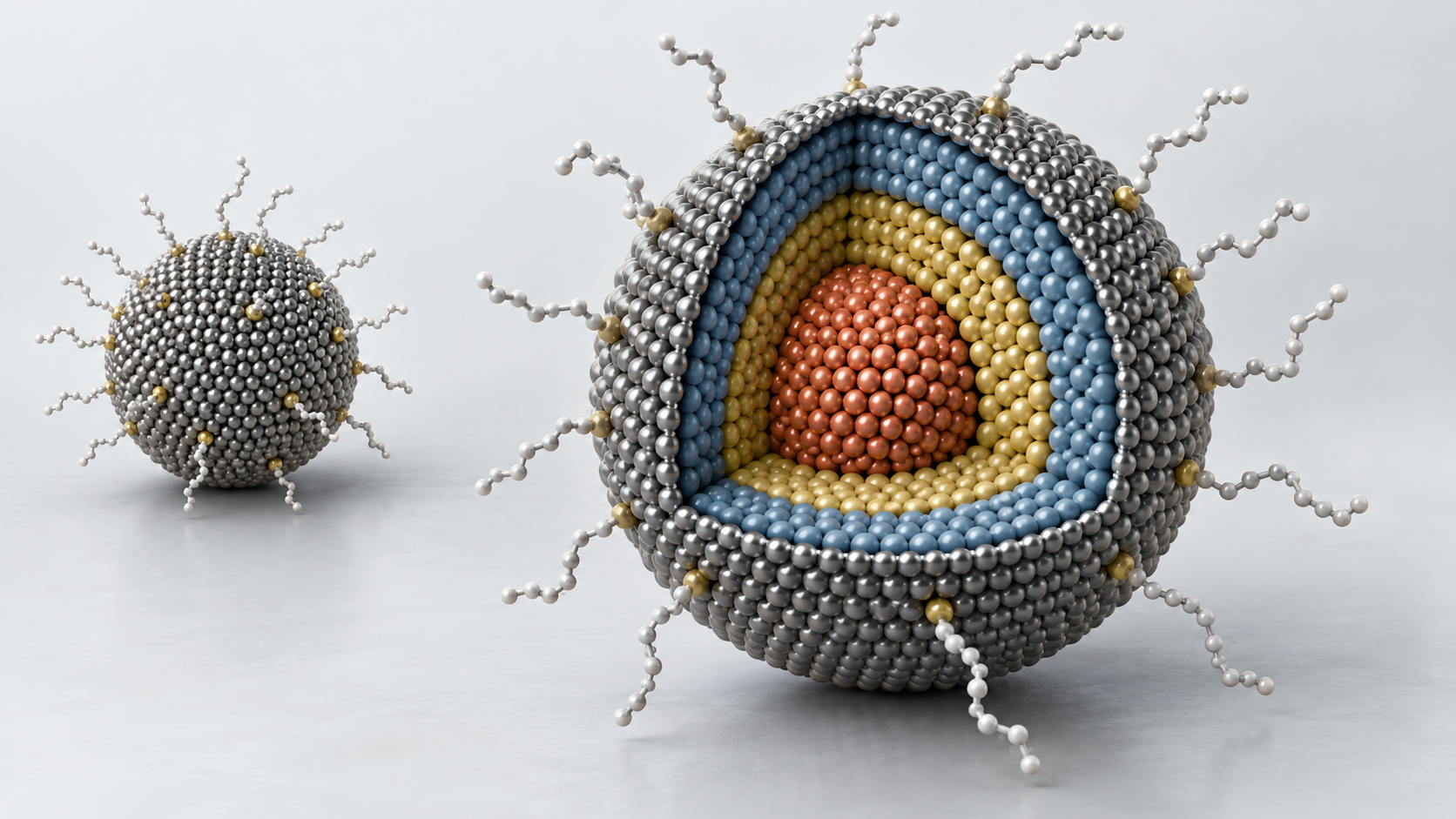
Shapes, colors and dimensions are illustrative. Consult the original schematic below for exact values and label correspondence.
View the original SVG schematic and exact annotations
Reading guide and original schematic labels: Core/shell cross-section and band diagram (concept) / Cross-section of an InP/ZnSe/ZnS-type dot (example) / Core (InP) / Inner shell (ZnSe) / Outer shell (ZnS) / ligands / Thicknesses and compositions are examples only / Band diagram (type I, schematic) / electron / hole / shell / core / shell / recombine, emit light / surface trap / surface trap / With a narrow-gap core and wide-gap shell (type I), / both carriers stay in the core, away from the surface / No energies shown; real band-edge positions differ. / Note: conceptual. Based on Hines and Guyot-Sionnest [Ref. 5], the Nobel Committee's scientific background [Ref. 2] / and Won et al. [Ref. 9]; it does not depict the structure of any real product.
(2) What quantum yield expresses
Quantum yield (PLQY, photoluminescence quantum yield) is the fraction of absorbed photons that are emitted as photons (a definition). The main loss route is non-radiative recombination, in which an electron or hole is caught at a defect on the surface or inside and the energy becomes heat. The shell exists to keep carriers away from those catching sites (Commentary).
Treat a surface layer one atom thick (assumed here to be 0.3 nm) as the “surface” of a spherical particle and compute the fraction of volume it occupies Our calculation. Fraction = 1 − (1 − 2 × 0.3 ÷ diameter)3.
- Diameter 2 nm: about 66% / 3 nm: about 49% / 4 nm: about 39% / 5 nm: about 32%
- 6 nm: about 27% / 10 nm: about 17% / 20 nm: about 9%
Assumptions and limits: This is an order-of-magnitude estimate that assumes an atomic layer 0.3 nm thick and a perfect sphere. Real crystals are polyhedra, and the figure varies with crystal facet and ligand coverage. Even so, in the size range of quantum dots, roughly a third of the atoms sit at the surface, which shows why surface states govern optical properties (consistent with the Nobel documents' statement that a high surface-to-volume ratio makes surface states dominate the electronic structure).
6. A materials engineer's view (2): a thicker shell is not always better
- Lattice mismatch and strain: Rafipoor et al. showed by Raman spectroscopy that when core and shell lattice constants differ, surface reconstruction at the interface produces compressive or tensile strain in core and shell, and the surface traps formed at the same time can harm emission. In InP/(Zn,Cd)Se, changing the shell composition shifts the strain from compressive to tensile, and the strain vanishes at the composition where the lattice constants match Sourced. Shell design is therefore not only what to wrap with but how to match the lattice (intermediate layers, alloys).
- Thickness and emission efficiency: Won et al. state that engineering the shell thickness suppresses energy transfer and Auger recombination (a process in which two excitons interact and one is lost), so luminescence efficiency stays high Sourced. A thicker shell moves carriers further from traps, but may be a disadvantage for charge injection; read this together with the ligand point in the next item (Commentary).
- Ligand length: The same paper replaced the initial ligand with a shorter one to improve charge injection Sourced. For simply emitting light, a thick shell and long ligands can be advantageous, but for emitting light electrically (or extracting current) a thin shell and short ligands are needed. The optimum differs by use even for the same particle (Commentary).
- Absorption per unit volume: In uses such as QD films and QD-OLED, where blue light is absorbed and converted to another colour, the core is what absorbs and the shell mostly adds volume. The thicker the shell, the more particles are needed for the same absorption (Commentary).
7. Synthesis: hot injection and large-batch synthesis
(1) The idea of hot injection
The Nobel Committee's scientific background describes the 1993 method of Bawendi and co-workers as follows. Organometallic reagents are injected into a hot, high-boiling coordinating solvent, where they pyrolyse immediately. The sudden rise in concentration causes abrupt supersaturation and nucleation at a well-defined moment. Injection brings a sudden drop in temperature and dilution of the precursors, so growth stops. After reheating to the growth temperature, slow growth and annealing proceed. Finally, particles are selected by purification and size-dependent precipitation. The resulting particles have a regular core structure, consistent surface derivatisation, an electronically passivated surface and a well-defined size set by temperature control during growth, and removing small aliquots during growth yields a whole series of particle sizes in a single run Sourced. The same document adds that this principle of temporally discrete nucleation followed by controlled growth was already known from the production of monodisperse colloids Sourced. The room-temperature luminescence quantum yield in 1993 was up to about 10% Sourced.
(2) Ideas for large-batch synthesis, and what remains hard
- Without injection: The 2008 method of Li and Reiss uses the difference in reactivity between the InP and ZnS precursors to make InP/ZnS by a single-step heating-up with no precursor injection (emission 480–590 nm, quantum yield 50–70%) Sourced.
- Rethinking the raw materials: Bang et al. used elemental phosphorus (P4), made by sublimating red phosphorus powder, as the precursor for InP@ZnS, demonstrated more than 6 g per batch, and reported a quantum yield of up to 60% after optimisation Sourced. Tessier et al. used indium halides and aminophosphines and reported conversion close to full yield relative to the indium precursor Sourced.
- Continuous flow: In 2003 Chan et al. synthesised CdSe nanocrystals continuously in chip-based microfluidic reactors, controlling size through temperature, flow rate and concentration, with size distributions comparable to conventional macroscale syntheses Sourced.
- The perovskite problem: The review by Dey et al. says hot injection is tedious, needs high temperature and an inert atmosphere, and limits cost-effective mass production Sourced.
Convert the 6 g per batch of Bang et al. into a particle count, assuming spheres 5 nm in diameter and a density of 4.5 g/cm³ (an assumption) Our calculation. Volume of one particle = 4/3 × π × (2.5 × 10⁻⁷ cm)3 ≈ 6.5 × 10⁻²⁰ cm³. Mass = volume × density ≈ 2.9 × 10⁻¹⁹ g. 6 g ÷ 2.9 × 10⁻¹⁹ g ≈ about 2 × 10¹⁹ particles.
Assumptions and limits: The diameter and density are assumed, and we did not confirm whether the paper's “6 g” includes ligands or shell. This is an order-of-magnitude estimate. Even so, it shows that the size and surface of particles on the order of 1019 must be made uniform in one reaction (Commentary).
8. A materials engineer's view (3): size spread becomes colour spread
Of the emission energy, the extra part due to quantum confinement depends strongly on particle size (the 1/R² of Chapter 2). Assume that extra part is 0.5 eV and the emission is centred at 550 nm, and estimate how far the emission peak moves when the diameter varies by ±5% Our calculation.
- A 5% change in diameter changes the 1/R² term by about 10% (for a small change, 2 × ΔR/R). Ten percent of 0.5 eV is 0.05 eV
- In wavelength, Δλ ≈ λ² × ΔE ÷ 1239.84 = 550² × 0.05 ÷ 1239.84 ≈ 12 nm
Assumptions and limits: The 0.5 eV extra energy is an assumption, not the value of a real quantum dot. Shifts caused by the shell, and spread in particle shape or composition, are ignored. Even so, figures such as an FWHM of 40 nm or less (Dabbousi et al.), 12–42 nm (Protesescu et al.) and 46–63 nm (Tessier et al.) can be read as the sum of the width of the size distribution and the particle-to-particle spread in composition and shape (Commentary). To obtain narrow emission, reproducibility of synthesis—making nucleation happen at a single instant—matters most, and that is exactly what becomes difficult at large scale.
Dabbousi et al. state that they determined size, size distribution, shape and internal structure by combining wavelength-dispersive X-ray spectroscopy, X-ray photoelectron spectroscopy, small- and wide-angle X-ray scattering, and transmission electron microscopy (TEM) Sourced. Yu et al. measured that the extinction coefficient at the first excitonic absorption peak of CdTe, CdSe and CdS nanocrystals depends strongly on size (between a square and a cubic dependence) Sourced. A TEM diameter, a size converted from an absorption peak, and a hydrodynamic diameter from dynamic light scattering give different values even for the same sample, so when comparing sizes check what was used to measure them (Commentary).
9. Applications: QD films, QD-OLED and electroluminescent QLED
There are three ways of using quantum dots in displays, differing in how the light is produced. Names vary between companies and documents, so this article separates them by what makes the dots glow (our own organisation).
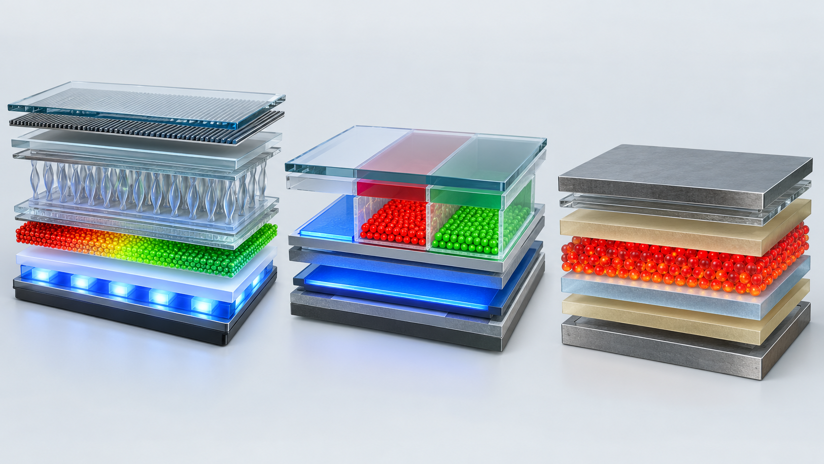
Shapes, colors and dimensions are illustrative. Consult the original schematic below for exact values and label correspondence.
View the original SVG schematic and exact annotations
Reading guide and original schematic labels: Three ways of using quantum dots (layer structure, concept) / A QD film + LCD / B QD-OLED / C Electroluminescent QLED / LCD panel, colour filter / barrier film / QD layer (in resin) / barrier film / light guide + blue LEDs / Part of the blue light is / turned green and red to make white / Mechanism: photoluminescence / colour filter etc. / red QD / green QD / passes / QD conversion layer / blue OLED (all pixels) / Blue light is converted pixel by pixel / to red or green (blue passes) / Mechanism: OLED + colour conversion / cathode (electrode) / electron transport layer / QD layer (emitter) / hole transport layer / anode (electrode) / Electrons and holes are injected / and recombine inside the dots / Mechanism: electroluminescence / Note: conceptual. Layer thicknesses, order and materials are examples, not the structure of a real product. / A follows the QD-film patent [Ref. 23], B a book chapter on QD-OLED [Ref. 21] and C the paper by Won et al. [Ref. 9]; / all are generic descriptions.
(1) QD films and QD diffuser plates (liquid crystal displays)
In 2010 Jang et al. combined multiply passivated green and red quantum dots as colour converters with blue InGaN LEDs and reported external quantum efficiencies of 72% (green) and 34% (red). Their white QD-LED backlight had an efficacy of 41 lm/W and a colour reproducibility of 100% of the NTSC standard in CIE 1931, and they state that it was the first demonstration of a 46-inch LCD TV panel using such a backlight Sourced. In 2013 Luo, Chen and Wu calculated, from measured QD emission spectra for a blue-LED-pumped red and green quantum dot backlight, a colour gamut of 115% in CIE 1931 and 140% in CIE 1976 at the same energy efficiency as conventional backlights. They also showed a fundamental trade-off between system efficiency and colour gamut Sourced (an optical-model analysis, not measurements on a real display).
A book chapter on quantum dot enhancement film (QDEF) by Luo and Yurek calls QDEF “one of the first widespread consumer applications” of quantum dot technology. It states that QDEF was introduced in 2013, that it remains the predominant QD technology in use as of 2024 (including derived forms such as the QD diffuser plate), and that it had been integrated into over 70 million display devices by the end of 2024 Sourced. That figure is, however, a statement by the chapter's authors and not an independent statistic.
(2) QD-OLED (colour conversion)
A book chapter by Oh et al. says that commercial QD-OLED displays use quantum dot colour-conversion technology, and it covers QD ink, front-plane materials (bank, colour filter, low-refractive-index layer), panel structure and the inkjet printing process Sourced. Yet the efficiency of the conversion layer is not trivial. Byun et al. examined conversion efficiency of colour-conversion layers made by dispersing quantum dots in PDMS (silicone rubber) under blue OLED light: a layer of quantum dots alone leaked much blue (blue leakage) and had an output/input efficiency below 10%, whereas the PDMS-based layers reached a maximum of 30.0% at 8.3 wt% and a thickness of 35.9 µm Sourced. This is a laboratory value for one particular material, thickness and concentration, not the level of commercial products. One can read from it a design problem: absorbing the blue light fully requires a product of concentration and thickness, which collides with the thickness limit of a pixel (Commentary).
(3) Electroluminescent QLED (making the dots themselves glow electrically)
A device that makes quantum dots glow electrically was reported in 1994 as a light-emitting diode made from CdSe nanocrystals and a semiconducting polymer (from the title of the paper by Colvin et al.) Sourced. In 2019 Won et al. reported that QD-LEDs made from the InP/ZnSe/ZnS dots described above showed a theoretical maximum external quantum efficiency of 21.4%, a maximum brightness of 100,000 cd/m² and a lifetime of a million hours at 100 cd/m², comparable to state-of-the-art Cd-containing devices Sourced. The lifetime is the authors' statement; this article has not checked the full text for the evaluation conditions (measured or extrapolated).
The Nobel Prize announcement states that quantum dots “now illuminate computer monitors and television screens based on QLED technology” Sourced. In academic usage, however, “QLED (QD-LED)” most often means the device in which the dots are made to glow electrically (item (3) above), while the same word is also used as a product name for LCDs that change colour with a film (item (1)) (Commentary; usage differs from company to company, and this article does not go into individual product names). When reading a source, the quickest check is whether the quantum dots there glow when they receive light or when they receive current.
10. Reliability: weakness to oxygen, water, heat and light
(1) Photo-oxidation: in air the core shrinks and the colour moves
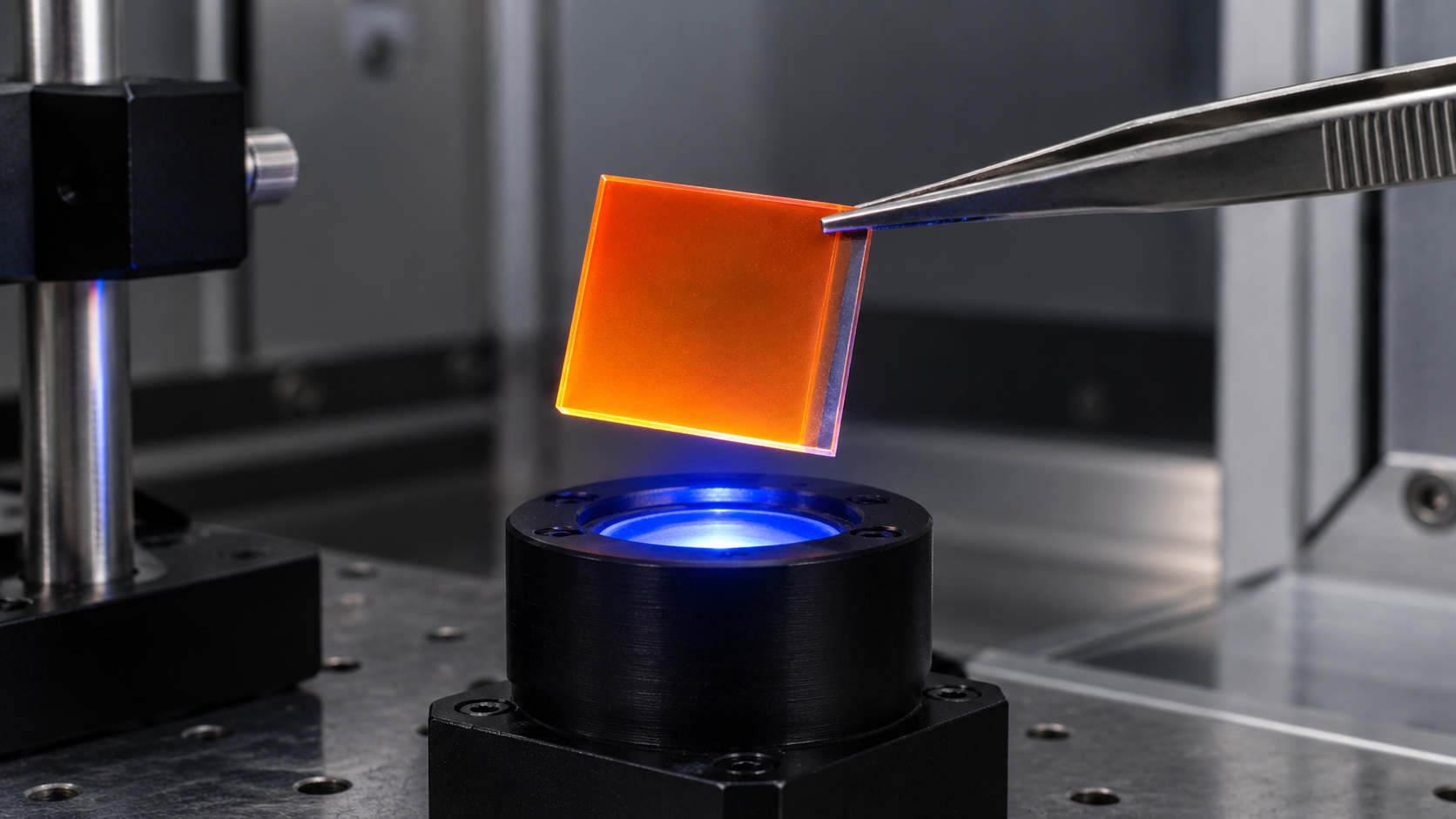
In 2001 van Sark et al. studied the room-temperature luminescence of single CdSe/ZnS core–shell quantum dots by spectrally and temporally resolved confocal microscopy. Under illumination in air, the emission wavelength shifted by about 30 nm towards the blue; in nitrogen, no shift was seen. The authors ascribed the shift to a shrinkage of the CdSe core by about 1 nm through photo-oxidation. Photobleaching was also about 4 times faster in air than in nitrogen, indicating the formation of non-radiative recombination centres during photo-oxidation Sourced. Because confinement is so sensitive to size (Chapters 2 and 8), the result that a core shrinking by only 1 nm moves the colour shows a built-in difficulty in keeping the colour of quantum dots stable (Commentary).
(2) Heat: emission falls and the colour shifts with temperature
Savchenko et al. studied the emission of an ensemble of InP/ZnS quantum dots with an average size of 2.1 nm over 6.5–296 K. They reported that as temperature rises, non-radiative relaxation channels (two, with activation energies of 95 meV and 16 meV) take effect and emission weakens, and that the chromaticity changes from yellow to yellow-green Sourced. This measurement covers cryogenic temperatures up to room temperature; it is not the behaviour at the higher temperatures at which LEDs and displays actually run. Reliability at real operating temperatures has to be established with tests under other conditions (Commentary).
(3) Water and oxygen: films fail from the edge
US Patent 10,167,417 B2 of 3M (priority date 3 July 2014, granted 1 January 2019) describes the structure and problems of QD film concretely Sourced.
- A laminate in which a layer of quantum dots dispersed in a matrix (resin) is sandwiched between two barrier layers. Quantum dots are highly sensitive to degradation, so excellent barrier properties against water and oxygen are needed
- Barrier materials include polymer films such as PET and oxides such as silicon oxide, titanium oxide and aluminium oxide; each barrier layer may consist of several sub-layers of different materials or compositions
- But at a cut edge the matrix is exposed to the atmosphere, and protection there depends on the barrier properties of the matrix itself. Ingress of water or oxygen from the edge produces a dark line (edge ingress) around the cut edge, which harms display performance
- The patent states that with conventional matrices edge ingress exceeded 1 mm after 100+ hours of accelerated aging, whereas the matrices it discloses limit edge ingress to less than 0.5 mm after aging at 65 °C/95% relative humidity or at 85 °C, and keep the colour change to 0.02 or less (or even 0.005 or less) in CIE 1931 (x, y). The quantum dot layer is stated to be about 40–400 µm thick (or about 80–250 µm)
These are targets and embodiments disclosed by the applicant (3M), not guaranteed values for products or a third-party assessment. Even so, they show a materials-side view in which lifetime is set not only by the durability of the quantum dot itself (the shells of Chapter 5) but by the barrier properties of the surrounding resin and the design of the laminate's edges (Commentary).
Apart from statements with a source, the following is commentary by this article.
- Particle side: shell thickness and lattice matching (Chapter 6), removal of the oxide layer (InP), strength of ligand binding. The review by Jang et al. states that for InP-based dots improving stability through control of inorganic and organic passivating structures is required Sourced.
- Matrix side: oxygen and water-vapour permeability (the patent gives upper limits for the oxygen permeation and water vapour transmission of the cured matrix), compatibility between dots and resin (to avoid aggregation), and cure shrinkage on cross-linking.
- System side: the multilayer barrier film (organic and inorganic oxide layers), edge sealing, and the heat and light intensity of the source.
- Perovskite systems: The review by Dey et al. says stability is one of the major roadblocks to practical use, and that surface-coating strategies against humidity, heat and harsh environments are being pursued Sourced.
In solar cells, on the other hand, Chuang et al. reported ZnO/PbS quantum dot solar cells made by room-temperature solution processing whose unencapsulated devices showed no change in performance after more than 150 days of storage in air Sourced (Chapter 12). The “weakness” of quantum dots varies greatly with composition, surface treatment and use, and cannot be summed up in one sentence (Commentary).
11. Cadmium regulation (the EU RoHS Directive)
(1) The framework
The EU's RoHS Directive (Directive 2011/65/EU) restricts hazardous substances in electrical and electronic equipment. Cadmium is a restricted substance listed in its Annex II, with a maximum tolerated concentration of 0.01% by weight of cadmium in homogeneous materials Sourced. Applications listed in Annex III are exempt. Exemption decisions turn on conditions such as whether the reliability of substitutes is ensured and whether the benefits of substitution outweigh its negative environmental, health and consumer safety impacts Sourced (from the recitals of Delegated Directive 2024/1416). The restriction is by weight concentration and does not distinguish whether a particle is nano-sized (our summary).
(2) How the quantum dot exemption developed
Commission Delegated Directive (EU) 2017/1975 granted an exemption, as entry 39(a) of Annex III, for cadmium selenide in downshifting (colour-converting) semiconductor nanocrystal quantum dots used in display lighting applications. Its original expiry date was 31 October 2019. Because applications for amendment were submitted in 2017 and 2018, then under the Directive's rules the exemption remained valid until a decision on the renewal application was taken Sourced.
After evaluation studies (November 2020 and November 2022), the Commission amended entry 39 through Commission Delegated Directive (EU) 2024/1416 (dated 13 March 2024; published in the Official Journal on 21 May 2024) as follows Sourced.
| Entry | Scope | Limit (as written in the Directive) | Expiry |
|---|---|---|---|
| 39(a) (amended) | Cadmium selenide in downshifting cadmium-based semiconductor nanocrystal quantum dots for use in display lighting applications | Less than 0.2 µg Cd per mm² of display screen area | Expires for all categories on 21 November 2025 |
| 39(b) (new) | Cadmium in downshifting semiconductor nanocrystal quantum dots directly deposited on LED semiconductor chips, for use in display and projection applications | Less than 5 µg Cd per mm² of LED chip surface, with a maximum of 1 mg per device | Expires for all categories on 31 December 2027 |
Note: a summary of the Annex wording. The legally authoritative text is the original in the Official Journal of the European Union.
According to the recitals, the evaluation found the following Sourced.
- The so-called “on-edge” and “on-surface” configurations no longer meet the conditions for an exemption (the recitals do not define these configurations, and this article has not confirmed their definitions from primary sources). The “on-chip” configuration, with the dots placed directly on the LED chip, needs the least cadmium and performs better
- For lighting applications of on-chip dots, reliable substitutes with similar performance are currently available, and the benefits of an exemption would not outweigh its negative impacts
- For display applications there are also many alternatives, but for some specific technologies such as micro displays no reliable alternative yet exists
- Alternatives for cadmium quantum dot applications might be available by the end of 2027, and the expiry of the exemption was set to that date
(3) Adopted, applied, and what can be confirmed now
- Adopted: 13 March 2024 (a Commission delegated directive) / Published in the Official Journal: 21 May 2024 Sourced
- Entry into force: The Directive enters into force on the twentieth day following publication (counting from the publication date, 10 June 2024) Our calculation
- Application by Member States: laws to be adopted and published by 31 December 2024 and applied from 1 January 2025 Sourced
- Expiry of 39(a): 21 November 2025 (already past as of October 2026) Sourced
- Expiry of 39(b): 31 December 2027. Whether a renewal will be applied for or granted after that could not be confirmed within the scope of this article Not yet confirmed
This chapter covers only the EU RoHS exemption for quantum dots. A product that uses quantum dots must also be checked against the REACH Regulation, national laws, and the rules of other regions such as Japan, South Korea, China and the United States. This article did not look into these, and has not confirmed them. This article is not legal advice; the conformity of any specific product depends on the official documents and expert confirmation.
12. Quantum dot solar cells
Because the bandgap can be tuned by particle size, quantum dots have also been studied as light-absorbing materials for solar cells. The Nobel Committee's scientific background says photovoltaics is among the widely explored application areas of quantum dots, and that quantum dots may give access to bandgap ranges not easily accessible with other materials, such as in the infrared Sourced.
- PbS quantum dots: In 2014 Chuang et al. reported ZnO/PbS quantum dot solar cells with a certified efficiency of 8.55%, achieved by engineering the band alignment through ligand treatments, and unencapsulated devices whose performance remained unchanged for over 150 days of storage in air. The devices are made by room-temperature solution processing Sourced.
- CsPbI3 perovskite quantum dots: In 2017 Sanehira et al. reported that treatments with A-site cation halide salts (AX) doubled the charge-carrier mobility of the quantum dot films and gave a record certified quantum dot solar cell efficiency (at that time) of 13.43%. They state that the bandgap of the dots can be tuned between 1.75 and 2.13 eV, making them a candidate for the top cell of all-perovskite multijunction solar cells Sourced.
Sanehira et al. show that charge-carrier mobility in quantum dot films is dictated by the chemical conditions at the junctions between dots and that AX treatments give a way of tuning the coupling between dots Sourced. In solar cells, then, the distance between particles and the chemistry of the interfaces set performance. For light emission, by contrast, keeping particles apart and the surface inert (long ligands, thick shells) was an advantage (Chapter 6). A surface polished so a dot will glow can get in the way when it must conduct. This is why particle synthesis and the film-forming step (ligand exchange) are designed together (Commentary).
The two efficiencies above are certified values of their time; this article did not confirm device areas or details of the certifying body. Later records are mentioned in news and secondary sources with higher values, but they could not be confirmed in primary sources and are therefore not given here (Chapter 13). Whether any product using quantum dot solar cells is in volume production could also not be confirmed within the scope of this article.
13. What this article could not confirm, and a summary
- Quantum yield and size distribution of current cadmium-based quantum dots: The CdSe values quoted here (30–50%) come from 1990s papers. The level of current volume products could not be confirmed in published primary sources.
- Specifications of actual QD-OLED and QD film products: Manufacturers' production specifications (type of quantum dot, content, lifetime) could not be confirmed in primary sources. The numbers come from papers, a patent and book chapters, and the patent's figures are targets and embodiments disclosed by the applicant.
- Conditions for evaluating the lifetime in Won et al. (2019): Only the abstract was checked (measured or extrapolated).
- “Over 70 million” QDEF units: A statement by the authors of a book chapter, not an independent statistic.
- Regulation other than RoHS: REACH and the rules of Japan, South Korea, China, the United States and others were not examined. Treatment of entry 39(b) after the end of 2027 is also unconfirmed.
- Latest records and commercialisation of quantum dot solar cells: not confirmed in primary sources.
- Toxicity of quantum dots: not covered here. Results differ with composition, size, surface and solubility, so one cannot say “nano means dangerous” or “nano means safe”. For the debate about use as labels, see our explainer on nanoparticles and nanozymes.
- Colour is set by particle size; brightness and lifetime by surface and shell. Through quantum confinement, the smaller the particle, the further absorption and emission shift towards the blue Sourced
- Size spread is colour spread. Under stated assumptions, a ±5% spread in diameter corresponds to an emission peak spread of about ±12 nm Our calculation
- A shell keeps charge carriers away from surface traps. But the optimum of lattice matching, thickness and ligand length changes depending on whether the dot is to emit light or to carry current Sourced
- Synthesis means “making nucleation happen at a single instant”. There is the principle of hot injection, and large-batch approaches such as heating-up without injection and continuous flow Sourced
- Lifetime is decided not by the particle alone but by the surrounding resin and barrier. In QD films, ingress of water and oxygen from cut edges is a problem Sourced
- The EU RoHS Directive has narrowed the cadmium exemption for quantum dots. Entry 39(a) expired on 21 November 2025 and 39(b) runs until 31 December 2027 Sourced. Treatment after the end of 2027 is Not yet confirmed
14. Glossary
- Quantum dot
- A semiconductor nanocrystal small enough that its size determines its properties. Absorption and emission colour change with particle size.
- Quantum confinement
- The effect by which a small crystal confines electrons and holes, makes their energies discrete and widens the bandgap.
- Bandgap
- The range of energy that electrons cannot occupy. It sets the wavelength of absorption and emission.
- Exciton
- An excited electron and hole bound to each other as a pair.
- Core/shell
- A structure in which a light-emitting centre (core) is wrapped in a wider-bandgap material (shell).
- Ligand
- An organic molecule bound to the particle surface. It keeps the particles dispersed and passivates the surface.
- Quantum yield (PLQY)
- The fraction of absorbed photons that are emitted as photons.
- FWHM
- Full width at half maximum of an emission peak. The smaller it is, the higher the colour purity.
- Hot injection
- A synthesis in which precursors are injected into a hot coordinating solvent so nucleation happens at one instant and sizes come out uniform.
- Auger recombination
- A process in which two excitons interact and the energy of one recombination is passed to the other, losing the light.
- QDEF
- Quantum dot enhancement film. Placed in an LCD backlight to widen the colour gamut.
- Edge ingress
- Water and oxygen entering at a cut edge and degrading the quantum dots along it.
- RoHS Directive
- The EU directive (2011/65/EU) restricting hazardous substances in electrical and electronic equipment.
- On-chip configuration
- Quantum dots deposited directly on the LED chip. It is described as needing the least cadmium.
15. References (primary sources)
- The Royal Swedish Academy of Sciences The Nobel Prize in Chemistry 2023, press release — nobelprize.org
- The Nobel Committee for Chemistry Scientific Background to the Nobel Prize in Chemistry 2023: Quantum dots – seeds of nanoscience (4 October 2023) — nobelprize.org (PDF)
- Brus LE Electron–electron and electron-hole interactions in small semiconductor crystallites: The size dependence of the lowest excited electronic state. J Chem Phys 1984;80:4403–4409 — doi.org/10.1063/1.447218
- Murray CB, Norris DJ, Bawendi MG Synthesis and characterization of nearly monodisperse CdE (E = sulfur, selenium, tellurium) semiconductor nanocrystallites. J Am Chem Soc 1993;115:8706–8715 — doi.org/10.1021/ja00072a025
- Hines MA, Guyot-Sionnest P Synthesis and Characterization of Strongly Luminescing ZnS-Capped CdSe Nanocrystals. J Phys Chem 1996;100:468–471 — doi.org/10.1021/jp9530562
- Dabbousi BO et al. (CdSe)ZnS Core–Shell Quantum Dots: Synthesis and Characterization of a Size Series of Highly Luminescent Nanocrystallites. J Phys Chem B 1997;101:9463–9475 — doi.org/10.1021/jp971091y
- Li L, Reiss P One-pot Synthesis of Highly Luminescent InP/ZnS Nanocrystals without Precursor Injection. J Am Chem Soc 2008;130:11588–11589 — doi.org/10.1021/ja803687e
- Kim S et al. Highly Luminescent InP/GaP/ZnS Nanocrystals and Their Application to White Light-Emitting Diodes. J Am Chem Soc 2012;134:3804–3809 — doi.org/10.1021/ja210211z
- Won Y-H et al. Highly efficient and stable InP/ZnSe/ZnS quantum dot light-emitting diodes. Nature 2019;575:634–638 — doi.org/10.1038/s41586-019-1771-5
- Protesescu L et al. Nanocrystals of Cesium Lead Halide Perovskites (CsPbX3, X = Cl, Br, and I): Novel Optoelectronic Materials Showing Bright Emission with Wide Color Gamut. Nano Lett 2015;15:3692–3696 — doi.org/10.1021/nl5048779
- Tessier MD et al. Economic and Size-Tunable Synthesis of InP/ZnE (E = S, Se) Colloidal Quantum Dots. Chem Mater 2015;27:4893–4898 — doi.org/10.1021/acs.chemmater.5b02138
- Bang E et al. Large-Scale Synthesis of Highly Luminescent InP@ZnS Quantum Dots Using Elemental Phosphorus Precursor. Chem Mater 2017;29:4236–4243 — doi.org/10.1021/acs.chemmater.7b00254
- Cossairt BM Shining Light on Indium Phosphide Quantum Dots: Understanding the Interplay among Precursor Conversion, Nucleation, and Growth. Chem Mater 2016;28:7181–7189 — doi.org/10.1021/acs.chemmater.6b03408
- Rafipoor M et al. Strain Engineering in InP/(Zn,Cd)Se Core/Shell Quantum Dots. Chem Mater 2018;30:4393–4400 — doi.org/10.1021/acs.chemmater.8b01789
- Dey A et al. State of the Art and Prospects for Halide Perovskite Nanocrystals. ACS Nano 2021;15:10775–10981 — doi.org/10.1021/acsnano.0c08903
- Chan EM, Mathies RA, Alivisatos AP Size-Controlled Growth of CdSe Nanocrystals in Microfluidic Reactors. Nano Lett 2003;3:199–201 — doi.org/10.1021/nl0259481
- European Commission Commission Delegated Directive (EU) 2024/1416 of 13 March 2024 amending Directive 2011/65/EU as regards an exemption for cadmium in downshifting quantum dots directly deposited on LED semiconductor chips (Official Journal, 21 May 2024) — eur-lex.europa.eu
- Jang E et al. White-Light-Emitting Diodes with Quantum Dot Color Converters for Display Backlights. Adv Mater 2010;22:3076–3080 — doi.org/10.1002/adma.201000525
- Luo Z, Chen Y, Wu S-T Wide color gamut LCD with a quantum dot backlight. Opt Express 2013;21:26269 — doi.org/10.1364/oe.21.026269
- Luo ZS, Yurek J Quantum Dot Enhancement Film. In: Quantum Dot Display Science and Technology, Wiley 2025, pp. 131–166 — doi.org/10.1002/9781394181889.ch04
- Oh K et al. Quantum Dot (QD) Color Conversion for QD-Organic Light-Emitting Diode. In: Quantum Dot Display Science and Technology, Wiley 2025, pp. 197–230 — doi.org/10.1002/9781394181889.ch06
- Byun S-U et al. Polydimethylsiloxane-Based Quantum Dot Color Conversion Layers for QD-OLED Applications. Micromachines 2026;17:505 — doi.org/10.3390/mi17050505
- 3M Innovative Properties Co. US Patent 10,167,417 B2, Quantum dot article with reduced edge ingress and improved color stability (priority 3 July 2014; granted 1 January 2019) — patents.google.com
- van Sark WGJHM et al. Photooxidation and Photobleaching of Single CdSe/ZnS Quantum Dots Probed by Room-Temperature Time-Resolved Spectroscopy. J Phys Chem B 2001;105:8281–8284 — doi.org/10.1021/jp012018h
- Savchenko SS, Vokhmintsev AS, Weinstein IA Photoluminescence thermal quenching of yellow-emitting InP/ZnS quantum dots. AIP Conf Proc 2018;2015:020085 — doi.org/10.1063/1.5055158
- Chuang C-HM et al. Improved performance and stability in quantum dot solar cells through band alignment engineering. Nat Mater 2014;13:796–801 — doi.org/10.1038/nmat3984
- Sanehira EM et al. Enhanced mobility CsPbI3 quantum dot arrays for record-efficiency, high-voltage photovoltaic cells. Sci Adv 2017;3:eaao4204 — doi.org/10.1126/sciadv.aao4204
- Jang E et al. Environmentally Friendly InP-Based Quantum Dots for Efficient Wide Color Gamut Displays. ACS Energy Lett 2020;5:1316–1327 — doi.org/10.1021/acsenergylett.9b02851
- Colvin VL, Schlamp MC, Alivisatos AP Light-emitting diodes made from cadmium selenide nanocrystals and a semiconducting polymer. Nature 1994;370:354–357 — doi.org/10.1038/370354a0
- Yu WW, Qu L, Guo W, Peng X Experimental Determination of the Extinction Coefficient of CdTe, CdSe, and CdS Nanocrystals. Chem Mater 2003;15:2854–2860 — doi.org/10.1021/cm034081k
- Efros AL, Brus LE Nanocrystal Quantum Dots: From Discovery to Modern Development. ACS Nano 2021;15:6192–6210 (further reading; this article quotes no numbers from it) — doi.org/10.1021/acsnano.1c01399
16. Claim-to-source audit
| Claim in the text | Basis | Label |
|---|---|---|
| That quantum dots are particles so small that size determines their properties; that in the early 1980s Yekimov showed size-dependent quantum effects in copper chloride particles in glass, shortly afterwards Brus did so in particles in a liquid, and in 1993 Bawendi revolutionised chemical production; and the statement that quantum dots illuminate monitors and televisions based on QLED technology | Reference 1 https://www.nobelprize.org/prizes/chemistry/2023/press-release/ | Sourced |
| The present-day definition of a quantum dot (quantum size effects, many-body interactions such as excitons, or surface states dominating through a high surface-to-volume ratio). The hot-injection procedure (injection into a hot coordinating solvent, one-instant nucleation, temperature drop halting growth, reheating for growth, size-selective precipitation) and the quantum yield of up to about 10% in 1993. That aliquots taken during growth give many sizes. That CdSe/ZnS reached a quantum yield of up to 50% and that the shell keeps charge away from surface states. That the Murray et al. absorption spectra span about 12 to 115 Å. Photovoltaics as a widely explored application and quantum dots reaching otherwise hard-to-access bandgap ranges | Reference 2 https://www.nobelprize.org/uploads/2023/10/advanced-chemistryprize2023.pdf | Sourced |
| That Brus treated the lowest excited state of crystallites of about 50 Å with the effective-mass approximation and Coulomb interactions and gave an approximate formula determined by bulk properties with no adjustable parameters | Reference 3 https://doi.org/10.1063/1.447218 | Sourced |
| That the paper reports synthesis of nearly monodisperse CdE (S, Se, Te) crystallites | Reference 4 https://doi.org/10.1021/ja00072a025 | Sourced |
| That CdSe of 27–30 Å capped with ZnS (about 6 ± 3 Å) reaches a room-temperature quantum yield of 50% and that the cap removes surface traps | Reference 5 https://doi.org/10.1021/jp9530562 | Sourced |
| (CdSe)ZnS core diameters 23–55 Å, blue to red, FWHM of 40 nm or less, quantum yield 30–50% (room temperature); the techniques used to determine size and so on (WDX, XPS, small- and wide-angle X-ray scattering, TEM) | Reference 6 https://doi.org/10.1021/jp971091y | Sourced |
| InP/ZnS by single-step heating-up without precursor injection, emission 480–590 nm, quantum yield 50–70% | Reference 7 https://doi.org/10.1021/ja803687e | Sourced |
| InP/GaP/ZnS with maximum quantum yield 85% and testing in white LEDs | Reference 8 https://doi.org/10.1021/ja210211z | Sourced |
| InP/ZnSe/ZnS: etching of the oxide layer with HF, ZnSe growth at 340 °C, quantum yield of about 100% (the authors' statement), suppression of energy transfer and Auger recombination through shell thickness, shorter ligands, maximum external quantum efficiency 21.4%, maximum brightness 100,000 cd/m², lifetime of a million hours at 100 cd/m² | Reference 9 https://doi.org/10.1038/s41586-019-1771-5 | Sourced |
| CsPbX₃ nanocubes (4–15 nm edge), emission 410–700 nm, FWHM 12–42 nm, quantum yield up to 90% | Reference 10 https://doi.org/10.1021/nl5048779 | Sourced |
| Synthesis from indium halides and aminophosphines, close to full yield relative to the indium precursor, emission 510–630 nm, FWHM 46–63 nm | Reference 11 https://doi.org/10.1021/acs.chemmater.5b02138 | Sourced |
| InP@ZnS from elemental phosphorus P₄ at more than 6 g per batch, quantum yield up to 60% | Reference 12 https://doi.org/10.1021/acs.chemmater.7b00254 | Sourced |
| The lag in InP synthesis attributed to the difficulty of controlling nucleation and crystallisation, and the build-up of magic-size nanoclusters | Reference 13 https://doi.org/10.1021/acs.chemmater.6b03408 | Sourced |
| Strain and surface traps from core/shell lattice mismatch; in InP/(Zn,Cd)Se the strain moves from compressive to tensile with shell composition and vanishes where lattice constants match (Raman spectroscopy) | Reference 14 https://doi.org/10.1021/acs.chemmater.8b01789 | Sourced |
| That stability of halide perovskite nanocrystals is a major roadblock to real-world applications, that hot injection is tedious, needs high temperature and an inert atmosphere and limits mass production, and surface-coating strategies against humidity and heat | Reference 15 https://doi.org/10.1021/acsnano.0c08903 | Sourced |
| Continuous synthesis of CdSe nanocrystals in microfluidic reactors, size controlled by temperature, flow rate and concentration, with a size distribution comparable to conventional macroscale synthesis | Reference 16 https://doi.org/10.1021/nl0259481 | Sourced |
| RoHS Annex II maximum cadmium concentration of 0.01% by weight in homogeneous materials; the conditions for Annex III exemptions; the grant of entry 39(a) by Delegated Directive 2017/1975 and its original expiry (31 October 2019), and its remaining valid pending a decision on renewal; the evaluation studies (November 2020 and November 2022); the amendment of 39(a) (0.2 µg Cd/mm², expiry 21 November 2025) and new 39(b) (5 µg Cd/mm², 1 mg per device, expiry 31 December 2027) by Delegated Directive 2024/1416 (13 March 2024; Official Journal 21 May 2024); application by Member States (adopted by 31 December 2024, applied from 1 January 2025); the evaluation conclusions (advantage of on-chip, substitutes for lighting, none yet for micro displays, substitutes possibly by the end of 2027) | Reference 17 https://eur-lex.europa.eu/eli/dir_del/2024/1416/oj | Sourced |
| External quantum efficiencies of 72% and 34% from green and red QD colour converters on blue InGaN LEDs, 41 lm/W, 100% of NTSC (CIE 1931), a 46-inch LCD TV panel demonstration | Reference 18 https://doi.org/10.1002/adma.201000525 | Sourced |
| Gamuts of 115% (CIE 1931) and 140% (CIE 1976) for a blue-LED-pumped red and green QD backlight, the same energy efficiency as conventional backlights, and the trade-off between efficiency and gamut (analysis from measured spectra) | Reference 19 https://doi.org/10.1364/oe.21.026269 | Sourced |
| That QDEF was introduced in 2013, remains the predominant QD technology as of 2024 and had been integrated into over 70 million display devices by the end of 2024 (the chapter authors' statement) | Reference 20 https://doi.org/10.1002/9781394181889.ch04 | Sourced |
| That commercial QD-OLED displays use QD colour conversion, and the chapter's coverage of QD ink, bank, colour filter, low-refractive-index layer and inkjet printing | Reference 21 https://doi.org/10.1002/9781394181889.ch06 | Sourced |
| PDMS-based colour-conversion layers: QD-only layers leaked much blue with an output/input efficiency below 10%; maximum 30.0% at 8.3 wt% and 35.9 µm | Reference 22 https://doi.org/10.3390/mi17050505 | Sourced |
| The laminate structure of QD film (two barrier layers and a QD layer in a matrix), barrier materials (PET, oxides), edge ingress and dark lines at cut edges, conventional edge ingress above 1 mm versus below 0.5 mm in the disclosed examples (65 °C/95% RH, 85 °C), colour change of 0.02 or less, layer thickness 40–400 µm, the applicant (3M), priority and grant dates | Reference 23 https://patents.google.com/patent/US10167417B2/en | Sourced |
| That in air under illumination the emission of single CdSe/ZnS dots shifts about 30 nm to the blue because the core shrinks by about 1 nm, and photobleaching is about 4 times faster than in nitrogen | Reference 24 https://doi.org/10.1021/jp012018h | Sourced |
| Emission of InP/ZnS (average 2.1 nm) at 6.5–296 K, non-radiative relaxation channels with activation energies of 95 meV and 16 meV, and the change of chromaticity | Reference 25 https://doi.org/10.1063/1.5055158 | Sourced |
| Certified efficiency of 8.55% for ZnO/PbS quantum dot solar cells, and no change in unencapsulated devices after more than 150 days in air | Reference 26 https://doi.org/10.1038/nmat3984 | Sourced |
| Certified efficiency of 13.43% for CsPbI₃ quantum dot solar cells, bandgap tunable between 1.75 and 2.13 eV, AX treatment doubling film mobility, and mobility being dictated by the chemistry at the junctions between dots | Reference 27 https://doi.org/10.1126/sciadv.aao4204 | Sourced |
| The factors governing the optical properties of InP-based quantum dots (core uniformity, thickness and shape of the ZnSe shell, electron and hole distribution, dangling bonds, oxidative phase, stacking faults, ligands) and the need to improve stability by controlling inorganic and organic passivating structures | Reference 28 https://doi.org/10.1021/acsenergylett.9b02851 | Sourced |
| That a light-emitting diode made from CdSe nanocrystals and a semiconducting polymer was reported in 1994 (from the title of the paper) | Reference 29 https://doi.org/10.1038/370354a0 | Sourced |
| That the extinction coefficient at the first excitonic absorption peak of CdTe, CdSe and CdS depends strongly on size (between a square and a cubic dependence) | Reference 30 https://doi.org/10.1021/cm034081k | Sourced |
| The idea of quantum confinement (the smaller the particle, the wider the bandgap), the guide that the confinement term scales as 1/R², and how colour moves | this article (commentary) | Commentary |
| Conversion between wavelength and photon energy (E ≈ 1239.84 ÷ λ): blue 450 nm about 2.76 eV, green 520 nm about 2.38 eV, red 630 nm about 1.97 eV, a difference of about 0.79 eV | our own calculation | Our calculation |
| Fraction of the surface layer (one atomic layer, assumed 0.3 nm): diameter 2 nm about 66%, 3 nm about 49%, 4 nm about 39%, 5 nm about 32%, 6 nm about 27%, 10 nm about 17%, 20 nm about 9% | our own calculation | Our calculation |
| That 6 g of InP@ZnS corresponds to about 2 × 10¹⁹ particles under the assumptions of 5 nm diameter and 4.5 g/cm³ | our own calculation | Our calculation |
| That under the assumptions of ±5% diameter, 0.5 eV of confinement energy and a 550 nm centre, the emission peak moves by about ±12 nm | our own calculation | Our calculation |
| That the date of entry into force, twenty days after publication on 21 May 2024, is 10 June 2024 | our own calculation | Our calculation |
| The organisation of each material's “headaches”, the trade-offs among shell thickness, ligands and lattice matching, the organisation of the term “QLED”, the view that quantum dot lifetime is decided by particle, resin and system, and the view that the best ligand for emitting light and for conducting current is opposite | this article (commentary) | Commentary |
| Treatment of entry 39(b) after 31 December 2027 (renewal applications and decisions), regulation other than RoHS, the latest efficiency records of quantum dot solar cells, and the quantum yield of current cadmium-based quantum dots | could not be confirmed within the scope of this article (our own note) | Not yet confirmed |
Last updated October 2026. Sources are limited to primary material (official Nobel Prize documents, EU legislation, peer-reviewed papers and a patent specification). CdSe quantum yields and similar values from 1990s papers show the level of their day, not the level of current volume products. The figures in the QD-film patent are targets and embodiments disclosed by the applicant, not guaranteed values for products. Because the article includes structural readings and materials-design interpretations, those are marked as Commentary and kept separate from sourced fact. The quantum yield of current cadmium-based quantum dots, regulation other than RoHS, treatment of entry 39(b) after the end of 2027, and the latest records for quantum dot solar cells are not covered, because they could not be confirmed in primary sources. This article explains materials, principles and regulation. It does not rank any product or company, and it is not legal advice. The hero image and Fig. 6 are AI-generated images and the other figures are vector drawings; none of them shows a real instrument, product or measurement result.