TECHNOLOGY EXPLAINER
Resists and Photomasks
— the light-sensitive film and the original set the limits of EUV
The light of lithography becomes a pattern only when it strikes the resist on the wafer. The resist is a film whose properties change with light, and the photomask is the original that carries the pattern. In EUV there are few photons, and the resist absorbs only a fraction of them. So a tug-of-war among sensitivity, resolution and line-edge roughness (LER), and stochastic defects from fluctuations in photon numbers, move to the front. This article sorts out chemically amplified and metal-oxide resists and the materials of reflective masks and pellicles, keeping the origin of each number clear.
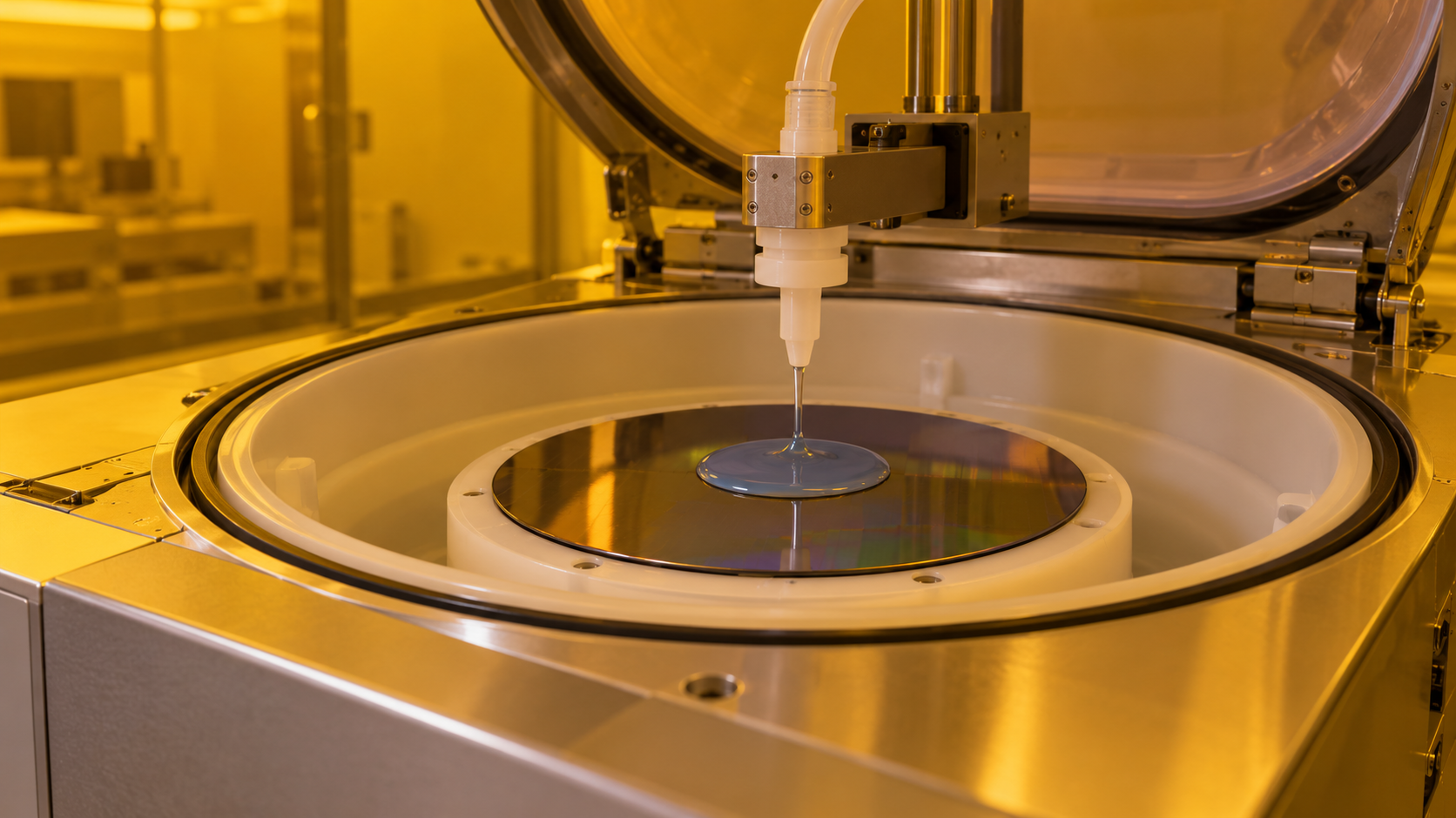
- What resists and photomasks are (the short version)
- What the resist does: carry the pattern and become the template
- Chemically amplified resists (CAR): one acid, many reactions
- What changes in EUV: light is absorbed by atoms
- Metal-oxide resists and dry resists
- The tug-of-war among sensitivity, resolution and line-edge roughness
- Stochastic defects
- The photomask: reflector and absorber
- Pellicle materials
- How to read the numbers
- Limits / Glossary / References / Claim-to-source audit
Sourced = a statement in published material (link given)
Our calculation = a figure this article derived, with the assumptions spelled out
Not yet confirmed = a plan or target with no confirmed track record
Structural readings and materials-design interpretations are marked separately as Commentary. Inference marks our own view that primary sources could not confirm.
Performance figures are written together with what was measured (method, sample) and at what level (simulation, laboratory, production).
This is an explainer on the principles and evaluation of semiconductor manufacturing materials. It does not rank any company, product or material. Company figures are the companies' own stated values and are separate from the yields of real fabs.
1. What resists and photomasks are (the short version)
A resist is a film whose solubility changes with light; a photomask (reticle) is an original with a pattern that transmits, blocks or reflects light. As our explainer on lithography and EUV showed, EUV works at 13.5 nm with little light, so these two materials strongly shape tool performance.
- The invention of chemical amplification: Ito (2000) states that the chemical amplification concept was invented at IBM Research and quickly brought into DRAM production, and that it has remained an important foundation for designing advanced resist systems for short-wavelength (below 300 nm) lithographySourced
- The resist works differently in EUV: in DUV the photoacid generator (PAG) absorbs the light directly, whereas in EUV the photon energy is large, 92 eV, so electrons in atoms are excited and a cascade of photo- and secondary electrons causes the reactions (Hasan et al., 2024 review)Sourced
- The reflective mask: an EUV mask is a Mo/Si multilayer reflector with a light-absorbing pattern (absorber) on top. For 0.33 NA tools the absorber is TaBN, typically 60 to 70 nm thick (Li et al., 2026)Sourced
EUV photons are few, and an organic resist absorbs only part of them. The review states that an organic resist about 35 nm thick uses only about 15% of the incident lightSourced. The fewer photons are absorbed, the more the fluctuation in their number (shot noise) shows in the result. Whether to make the resist absorb more light or react to fewer photons is the center of materials development (this article's commentary).
The previous article, lithography and EUV, covers the source, mirrors and photon counts; the next two, atomic layer deposition and etching, cover building and removing films. The resist sits between them: it turns what light drew into a form that etching can use.
2. What the resist does: carry the pattern and become the template
The resist flow is coat and bake, expose, develop. The film left after development becomes the mask (template) for etching. If exposure makes it more soluble the resist is positive tone; if it becomes less soluble (stays), negative tone.
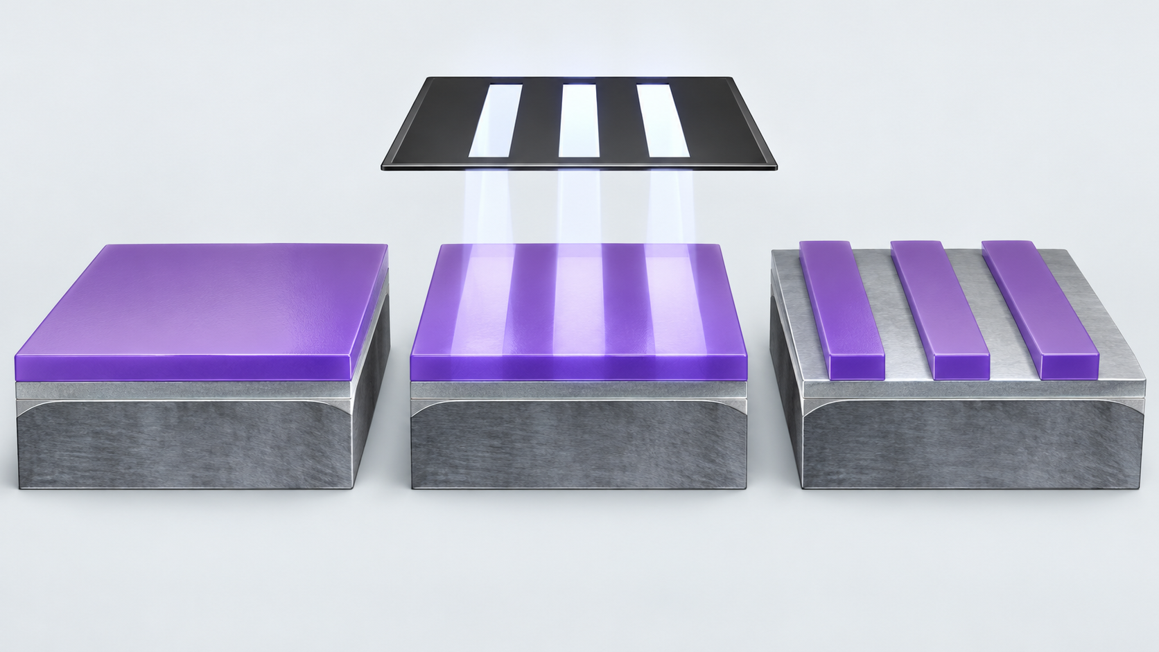
Shapes, colors and dimensions are illustrative. Consult the original schematic below for exact values and label correspondence.
View the original SVG schematic and exact annotations
Reading guide and original schematic labels: What the resist does: it carries the pattern and becomes the template (conceptual) / Cross-section sketch, positive tone as the example. Layer thicknesses are schematic. / 1. Coat and bake / Spin-coat resist over / the underlayer and bake / / 2. Expose / Light hits the pattern; / the exposed part changes / Light / 3. Develop / Exposed part dissolves; / a relief pattern forms / 4. Etch / Resist is the mask; / films below are etched / Resist / Underlayer / Substrate / Exposed region / * Positive: exposed areas dissolve. Negative: they stay. Metal-oxide resists reportedly cross-link on exposure [Source 1]. / * The underlayer provides anti-reflection, etch resistance and so on; real stacks differ by process (commentary).
In EUV the resist is applied thin. The review by Hasan et al. says that for higher resolution EUV resists are made thinner than in DUV, about 35 nm, to prevent pattern collapseSourced. A thinner film absorbs less light and leaves less margin to be etched away. That is the problem that runs through the rest of this article.
3. Chemically amplified resists (CAR): one acid, many reactions
A chemically amplified resist is a film whose main components are a polymer (carrying protecting groups that make it hard to dissolve) and a photoacid generator (PAG) that releases acid on exposure. Exposure makes acid; during the post-exposure bake (PEB) the acid moves and removes protecting groups one after another until the film dissolves in the developer. Because one acid works many times, it is called "amplification". Hasan et al. explain that in DUV the PAG absorbs the photon and is excited, and the chemistry that follows deprotects the polymer and changes its solubilitySourced.
The farther the acid moves, the more protecting groups one acid removes, and the higher the sensitivity. But each bit of travel also separates where the light struck from where the reaction occurred, and blurs the edge (this article's commentary). Kozawa (2019) used a simulation based on the reaction mechanisms of chemically amplified EUV resists to formulate the relations among resolution, line-edge roughness and sensitivity, and states that at half-pitches below 10 nm the effect of thermalized electrons becomes evident, and suppressing it requires a higher sensitizer concentration or a larger effective reaction radiusSourced (a theoretical study based on simulation). So as features shrink, the demand to reduce blur and the demand to keep sensitivity collide, which is the essential difficulty of chemical amplification (commentary). Real resists are tuned with additives that restrain acid diffusion (quenchers) and the like, but we did not confirm specific formulations in this article's scope.
4. What changes in EUV: light is absorbed by atoms
Hasan et al. state that EUV light interacts with the electrons of elements much more strongly than DUV interacts with molecular materialsSourced. Absorption of EUV is set almost entirely by the kinds and density of the elements in the resist. Organic resists made mostly of carbon, hydrogen and oxygen are fairly transparent to EUV, so a thin film uses only part of the incident light.
Taking absorbed fraction = 1 − exp(−α × thickness), where α is the EUV absorption coefficient, we look at a thickness of 35 nmOur calculation.
- Organic (assuming α = 4.8 /µm): at 35 nm, 1 − exp(−4.8 × 0.035) = about 15.5%, consistent with the review's "about 15% of the incident light"
- Absorption coefficient 3 times higher (α = 14.4 /µm): at the same 35 nm, about 39.6%
Assumptions and limits: in the review's text the unit of the absorption value was missing from the rendered page. We read it as µm⁻¹, consistent with 35 nm and about 15%, and set α = 4.8 /µm (an assumption that includes Inference). The "3 times" is an upper guide taken from Fallica et al. in the next section ("tin-based up to 3 times organic"), not a value for any specific resist.
As our explainer on lithography and EUV showed, at a dose of 30 mJ/cm² (the condition for the NXE:3800E throughput) about 2,000 photons are incident on a 10 nm × 10 nm area. Let us look at how many are absorbed, and the shot noise, as the thickness and absorption coefficient change.
Multiply the incident photons (about 2,039 at 30 mJ/cm², 10 nm × 10 nm) by the absorbed fraction, and take variation = 1 ÷ √(absorbed photons)Our calculation.
- Organic, 35 nm: about 315 absorbed photons → variation about 5.6%
- Absorption 3 times higher, 35 nm: about 807 → about 3.5%. Thickening the organic film to 50 nm gives only about 435 (about 4.8%)
Assumptions and limits: this is a guide from photon-count fluctuation only. Real variation is set together with chemical blur such as the spread of photo- and secondary electrons, acid diffusion and the non-linearity of dissolution, none of which is treated here. The 10 nm × 10 nm area is also our choice of example.
5. Metal-oxide resists and dry resists
The direct way to absorb more is to put in a metal that absorbs EUV well. The review by Hasan et al. says that transition metals and high-atomic-number metals and semimetals have large interaction cross-sections with EUV photons and are candidates for raising optical absorptionSourced.
Fallica et al. (2018, peer-reviewed) used a synchrotron-based method to measure the absorption of thin films of tin cage molecules and zirconium and hafnium oxoclustersSourced. The tin-based material absorbed up to three times as much as conventional organic resists, the hafnium-based about twice, and the zirconium-based about the same as organic polymer resists. The samples were research compounds, not commercial resists, and while measured values and values calculated from composition agreed fairly well, there were also substantial discrepancies from film density and thickness variationSourced.
| Family | How it works | Published strengths (category of source) | Issues and what we could not confirm |
|---|---|---|---|
| Chemically amplified resist (CAR) | Acid catalytically removes protecting groups from the polymer. Includes PAG, quencher and so on | Invented at IBM, brought into DRAM manufacturing, a foundation of advanced resist design (Ito) | In EUV, high doses tend to be needed and slow throughput, the review saysSourced. Acid diffusion blurs the image (commentary) |
| Metal-oxide resists (tin-based and others) | Metal-containing molecules or clusters change on exposure and form a cross-linked inorganic network (review) | Absorption up to 3 times organic (Fallica et al., research compounds). High etch resistance and a tendency to high sensitivity (review) | Adoption and performance in volume production could not be confirmed. Handling of metal-containing materials: Inference (below) |
| Dry resists (Lam Research's approach) | The film is deposited by a dry (vapour-phase) process and developed dry (company announcement) | The company describes lower dose, higher resolution and 5 to 10 times less raw material (2020, company's stated claims) | A development-stage announcement. Adoption and results at customers could not be confirmed Not yet confirmed |
Sources: Hasan et al. [Source 1], Fallica et al. [Source 2], Ito [Source 7], Lam Research announcement (26 February 2020) [Source 8]. Categories are given in the columns.
In its announcement of 26 February 2020, Lam Research said it was developing a dry resist with ASML and imec, and positioned it as extending the company's deposition and etch technology into photosensitive materials. It said the technology allows a lower dose and higher resolution and uses five to ten times less raw material (the company's claims at the development stage in 2020)Sourced. If the resist moves from a material you coat to a material you deposit, it enters the same tool world as the next two articles, atomic layer deposition and etching, which is what makes it interesting from this series' viewpoint (commentary).
As a research result for tin-based materials, researchers at Inpria reported the EUV photolithographic properties of tin-oxo clusters (Cardineau et al., 2014, peer-reviewed)Sourced. We did not check the individual values in that paper.
Resist design must satisfy many conditions at once: (1) absorb EUV well (by adding metals), (2) stay standing when coated thin, and (3) survive etching even when thin (high cross-linking, inorganic content). The review frames metal-oxide resists as favourable on (1) and (3), with high absorption and high etch resistanceSourced. Because a thin film can still etch the layer below, the problem that "thinner means less absorption" is eased as well (commentary). On the other hand, as an Inference, films containing metals probably need stricter control of coating, development, edge cleaning, waste liquid and metal contamination inside tools than organic films do. We could not confirm primary sources on this point.
6. The tug-of-war among sensitivity, resolution and line-edge roughness
Resist performance is discussed in terms of resolution, line-edge roughness (LER: the unevenness of a line's edge) and sensitivity, called the RLS trade-off after the initials. Kozawa et al. (2019) say these three relationships are an important concern for the extendability of EUV lithography, and formulated them by simulating chemically amplified resists. They use a "chemical gradient" as the LER indicator and examined its dependence on half-pitch, sensitizer concentration and the effective reaction radius of deprotectionSourced (simulation). Azumagawa et al. (2020) report that over half-pitches of 5 to 16 nm the relations among resolution, chemical gradient, sensitivity, total sensitizer concentration and effective reaction radius could be predicted by regressionSourced (analysis).
Roughness is often measured as the variation of line width, LWR (3σ). As an example, we calculate its ratio to the line width CDOur calculation.
- With an LWR of 1.5 nm (3σ): about 9.4% at a CD of 16 nm, about 12.5% at 12 nm, about 18.8% at 8 nm
- With an LWR of 1.0 nm: about 6.3% at 16 nm, about 8.3% at 12 nm, about 12.5% at 8 nm
Assumptions and limits: the LWR values (1.0 and 1.5 nm) are examples this article set for the calculation, not measurements of any real resist. The point is only that, for the same roughness, the share of the line width grows as lines get thinner.
7. Stochastic defects
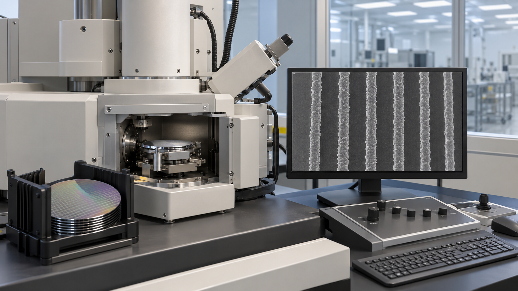
When photon and molecule numbers are small, results differ a little from place to place even under the same design and conditions. De Bisschop (2017, peer-reviewed) says these stochastic effects are measured as local variation of dimensions (line-width roughness and local CD uniformity, LCDU) and also appear as local, random printing failures such as missing contacts and small bridges in spaces (microbridges)Sourced. Where a failure occurs there is no reliable CD, so ordinary CD measurement cannot evaluate it. The paper proposes an index called NOK (not OK), which detects and counts failures from SEM images, and says dependence on CD, pitch, resist and dose can be studied experimentallySourced. It also looks at the feasibility of simple predictors that tell, at the mask OPC verification stage, which structures are sensitive to stochastic effectsSourced.
A chip has billions of lines and holes. Even if nearly every place is as designed, one rarely occurring failure can stop a chip from working (this article's commentary). So resist evaluation must look not only at average dimensions and roughness but at how often failures occur (the region of very low probability). That is why De Bisschop's index counts failures rather than measuring CD [Source 5]. Materials-side countermeasures include absorbing more (Figs. 4 and 5), raising the number of events that contribute to the reaction, restraining the spread of acid and molecules, and reducing pattern collapse and undissolved residue (design of development and rinse). The effect and cost of each depends on the specific material and conditions, and we do not generalize further here.
8. The photomask: reflector and absorber
Li et al. (2026, peer-reviewed, open access) describe the EUV mask as followsSourced. Because EUV is strongly absorbed by matter, the scanner uses reflective optics, and the mask follows the same reflective principle. A Mo/Si multilayer acts as the reflector, its layer thicknesses controlled precisely so that reflections add constructively. Illumination arrives at a small oblique angle, so that incoming and reflected light can be separated inside the optics. The substrate is low-thermal-expansion glass, which limits pattern distortion during exposure. On top, a patterned absorber that absorbs EUV strongly defines the circuit layout and raises image contrast. For 0.33 NA tools the advanced absorber is TaBN, typically 60 to 70 nm thick.
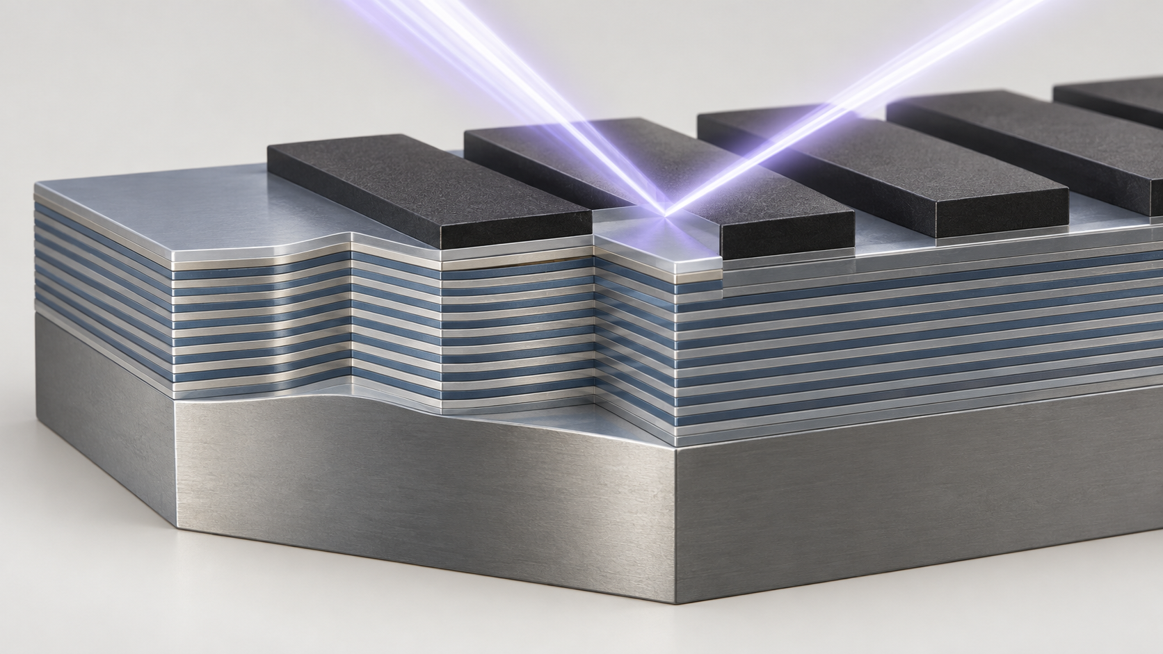
Shapes, colors and dimensions are illustrative. Consult the original schematic below for exact values and label correspondence.
View the original SVG schematic and exact annotations
Reading guide and original schematic labels: Cross-section of a reflective photomask (conceptual) / Layer thicknesses and ray angles are schematic. Light comes in at an angle and leaves at an angle. / Pellicle (dust membrane) / Incident / Reflected / shadow / Absorber / Capping layer / Mo/Si multilayer / Low-expansion glass / * Structure (substrate, Mo/Si multilayer, absorber), oblique incidence and TaBN at 60–70 nm (0.33 NA): Li et al. [Source 6]. / * The shadow stands for one cause of the mask 3D effect. Real layer counts, thicknesses and materials are not shown.
The mask 3D effect, and rethinking the absorber for High-NA
Because the light arrives at an angle, the absorber's thickness casts a shadow and distorts the image. This is called the mask 3D (M3D) effect. Li et al. say M3D arises from the combination of oblique incidence, complex reflections within the multilayer and the optical response of the absorber, and worsens as NA risesSourced. ASML's EXE:5000 page says that High-NA (0.55) uses anamorphic optics so that traditionally sized reticles can still be used [Source 12]Sourced. Meanwhile, absorbers that resist M3D have become a research focus.
Li et al. say that materials with a high EUV extinction coefficient (high-k) and a low refractive index (low-n) are thought to suppress M3D even when thin, and cite research examplesSourced.
- Ni-Al alloy (Luong et al.): allows a thinner absorber with better imaging and a larger process window, but stability and etchability need improvement
- Ta-Co alloy (Thakare et al.): raises image contrast and reduces best-focus variation, but brings a telecentricity-error problem
- Ru/Ta bilayer (Thakare et al.): balances etchability and imaging, but the bilayer complicates mask inspection and repair
- Pt-W alloy (Li et al. themselves): platinum-based, with tungsten added because it forms volatile products in fluorine plasma, which improves etchability. Simulation with optically characterized films indicated better imaging than TaBN at a smaller thickness. This is a simulation-centred evaluation by one research group, not adoption in real tools
The film requirements Li et al. list for mask absorbers are all familiar to materials engineersSourced.
- Deposition below 150 °C: to protect the reflectivity of the multilayer beneath
- Amorphous or nanocrystalline: to keep line-edge roughness small
- Surface roughness under 0.5 nm and residual stress within ±300 MPa, and stability under thermal load in use and cleaning solutions
- Processability: it must be etchable in fluorine-based plasma
- Repair and inspection: current EUV masks are repaired by electron-beam-induced deposition and etching. For a new absorber the precursor used in repair must also meet the optical requirements and not react in later steps. Defect inspection with DUV light has low contrast, so bright-field inspection techniques must be developed
An optically ideal material is often hard to etch or repair (commentary). What this series calls etching and deposition knowledge bears directly on choosing mask materials.
9. Pellicle materials
A pellicle is an ultrathin dust-protection membrane stretched in front of the mask. The requirements are high EUV transmittance, no breakage at nanometre thickness, tolerance of high temperature and hydrogen radicals, and low reflectance (Choi et al.)Sourced. Numbers are given in our explainer on lithography and EUV, so here we sort out the families of materials.
| Material family | Published information (category of source) | Caution |
|---|---|---|
| Silicon-based membranes | Mitsui Chemicals says conventional EUV pellicles use silicon-based membranes and that it began commercial production under ASML licence in 2021 (company announcement)Sourced | New materials are said to be needed for High-NA and high-power (600 W or more) EUV (the company) |
| Metal silicide | Full size 110 × 144 mm, over 90% transmittance, under 0.04% reflectance, tensile strength above 2 GPa (Choi et al., 2024, a prototype membrane in the paper)Sourced | Evaluated for 400 W-class EUV. Adoption in volume production could not be confirmed |
| Carbon nanotube (CNT) | Claims 92% or above transmittance and light resistance for exposure power above 1 kW (Mitsui Chemicals, 2024, the company's stated values)Sourced | Volume facility is a plan (5,000 sheets per year, tentative completion December 2025). Operating status could not be confirmed Not yet confirmed |
Sources: Choi et al. [Source 11], Mitsui Chemicals [Source 10]. The measurement conditions and bases of transmittance differ, so these are not figures for ranking.
10. How to read the numbers: keep simulation, laboratory and stated values apart
| Number | What it is | Category | Caution |
|---|---|---|---|
| About 15% (35 nm) | Share of incident EUV used by an organic resist | Review (2024) / reproduced by our calculation | The unit of the absorption coefficient is inferred. Varies by resist |
| Up to 3× / about 2× / same | Absorption of tin-based / Hf-based / Zr-based relative to organic | Peer-reviewed paper (2018, measured) | Thin films of research compounds, not commercial resists. Measured and calculated values also differ |
| 5 to 10 times less | Raw material use of the dry resist | Company's stated claim (2020) | A development-stage claim. Results could not be confirmed |
| Half-pitch 5 to 16 nm; below 10 nm | Range of the RLS relation; the regime where thermalized-electron effects show | Theory and simulation (2019 to 2020) | Not measured values from real tools |
| LWR 1.0 / 1.5 nm | Roughness ratio examples used in the calculation | Assumption in our calculation | Not measurements |
| 60 to 70 nm | Typical TaBN absorber thickness for 0.33 NA tools | Peer-reviewed paper (2026) | Differs by maker and generation |
| Under 150 °C, under 0.5 nm, ±300 MPa | Example conditions for depositing a mask absorber | Peer-reviewed paper (2026) | Requirements cited in the Pt-W study; not a standard |
| Over 90% / 92% or above | EUV transmittance of pellicles | Peer-reviewed paper (2024) / company's stated value (2024) | Measurement conditions and bases differ |
11. Limits and what we could not confirm
(1) We could not confirm the adoption of resist and mask materials in volume production
From the primary sources we read, we could not confirm how far metal-oxide resists, dry resists, new absorbers or CNT pellicles are used in volume production. Company announcements mostly describe development or plans.
(2) We give no performance figures for specific resists
Measured sensitivity (dose), resolution and LER of specific resists vary greatly with conditions (scanner, pattern, thickness, development) and are hard to compare among public primary sources, so we do not include them. The numbers in this article are calculations with stated assumptions, or are kept to what papers and companies state.
(3) Regulation and safety are not covered
We did not check the relation of fluorinated compounds (PFAS) in resists and anti-reflective films to regulation, or the handling and waste control of metal-containing materials. PFAS and semiconductor regulation is taken up with the gas chemistry in the next article, on etching.
(4) Electron-beam writing and mask-making processes are not covered
We do not cover the process of writing mask patterns or the details of inspection and repair tools. Templates for nanoimprint, which does not rely on light, are covered in our explainer on self-assembly and nanoimprint.
- Chemically amplified resists work by acid removing protecting groups one after another; the concept was invented at IBM and brought into DRAM manufacturingSourced
- In EUV, photons are absorbed by atoms and electrons drive the reaction. A 35 nm organic resist uses only about 15% of the incident lightSourced. With 3 times the absorption the same thickness takes about 40%Our calculation
- Tin-based materials absorb up to 3 times as much as organic ones (measured on research compounds). Dry resists are a claim at the development stageNot yet confirmed
- Sensitivity, resolution and LER pull against each other, and below 10 nm half-pitch the effect of thermalized electrons shows (simulation)Sourced
- Stochastic defects appear in two ways, as dimensional variation and as random printing failures, and indices that count failures are usedSourced
- The mask is built of low-expansion glass, a Mo/Si multilayer and an absorber (TaBN, 60 to 70 nm); for High-NA the focus is on the shadow (M3D)Sourced
12. Glossary
- Resist
- A light-sensitive film whose solubility changes with light. After development it serves as the etch template.
- CAR
- Chemically amplified resist. Acid catalytically removes protecting groups.
- PAG
- Photoacid generator. A component that releases acid under light or electrons.
- PEB
- Post-exposure bake. The step in which the acid moves and the reaction proceeds.
- Positive / negative tone
- The exposed part dissolves / the exposed part stays.
- RLS
- Resolution, line-edge roughness (LER) and sensitivity.
- LER / LWR
- Unevenness of a line edge / variation of line width.
- LCDU
- Local CD uniformity. Variation in the size of features such as holes.
- Stochastic defect
- A random printing failure or dimensional variation caused by fluctuation in photon and molecule numbers.
- Metal-oxide resist
- An inorganic-type resist containing metals such as tin, Hf or Zr that absorb EUV strongly.
- M3D
- Mask 3D effect. Image distortion from oblique incidence and absorber thickness.
- Absorber
- The film on an EUV mask that absorbs EUV and forms the pattern, such as TaBN.
- Pellicle
- An ultrathin dust-protection membrane in front of the mask.
- OPC
- Optical proximity correction. Pre-correction of the original's pattern.
13. References (primary sources)
- Hasan MW et al. "Recent Advances in Metal-Oxide-Based Photoresists for EUV Lithography", Micromachines 15(9), 1122 (2024, peer-reviewed review) — doi.org/10.3390/mi15091122
- Fallica R et al. "Absorption coefficient of metal-containing photoresists in the extreme ultraviolet", J. Micro/Nanopattern. Mater. Metrol. 17(2), 023505 (2018, peer-reviewed) — doi.org/10.1117/1.JMM.17.2.023505
- Kozawa T "Theoretical study on trade-off relationships between resolution, line edge roughness, and sensitivity in resist processes for semiconductor manufacturing by extreme ultraviolet lithography", Jpn. J. Appl. Phys. 58(9), 096502 (2019, peer-reviewed) — doi.org/10.7567/1347-4065/ab37ff
- Azumagawa K, Kozawa T "Analysis of trade-off relationships between resolution, line edge roughness, and sensitivity in extreme ultraviolet lithography using lasso regression", Jpn. J. Appl. Phys. 59(7), 076501 (2020, peer-reviewed) — doi.org/10.35848/1347-4065/ab984e
- De Bisschop P "Stochastic effects in EUV lithography: random, local CD variability, and printing failures", J. Micro/Nanolith. MEMS MOEMS 16(4), 041013 (2017, peer-reviewed) — doi.org/10.1117/1.JMM.16.4.041013
- Li Z et al. "Evaluating an alternative Pt-W alloy as a low-n EUV mask absorber: Film properties and imaging performance", iScience 29(8), 116912 (2026, peer-reviewed, open access) — doi.org/10.1016/j.isci.2026.116912
- Ito H "Chemical amplification resists: History and development within IBM", IBM J. Res. Dev. 44(1.2), 119–130 (2000, abstract of the paper) — doi.org/10.1147/rd.441.0119
- Lam Research "Lam Research Unveils Technology Breakthrough for EUV Lithography", news release, 26 February 2020 — globenewswire.com
- Cardineau B et al. "Photolithographic properties of tin-oxo clusters using extreme ultraviolet light (13.5 nm)", Microelectronic Engineering 127, 44–50 (2014, peer-reviewed) — doi.org/10.1016/j.mee.2014.04.024
- Mitsui Chemicals "Mitsui Chemicals Sets up Production Facilities for CNT Pellicles to Be Used in Next-Gen EUV Lithography", news release, 28 May 2024 — jp.mitsuichemicals.com
- Choi M et al. "Development and optimization of metal silicide EUV pellicle for 400W EUV lithography", Nanotechnology 36(6), 06LT01 (2024, peer-reviewed) — doi.org/10.1088/1361-6528/ad902d
- ASML "TWINSCAN EXE:5000", product page (manufacturer's stated values), accessed 9 October 2026 — asml.com
- ASML "TWINSCAN NXE:3800E", product page (manufacturer's stated values), accessed 9 October 2026 — asml.com
14. Claim-to-source audit
| Claim in the text | Basis | Label |
|---|---|---|
| That the chemical amplification concept was invented at IBM Research, brought into DRAM manufacturing, and remains a foundation for advanced resist design for wavelengths below 300 nm | Ito (2000, abstract of the paper) [Source 7] https://doi.org/10.1147/rd.441.0119 | Sourced |
| That in DUV the PAG absorbs the photon and deprotection follows; that in EUV the photon energy is 92 eV and a cascade of photo- and secondary electrons drives the reaction; that EUV resists are about 35 nm thin to avoid pattern collapse; that an organic 35 nm film uses only about 15% of the incident light; that transition metals and high-atomic-number metals are candidates for raising EUV absorption; that metal-oxide resists form a cross-linked inorganic network, have high etch resistance and tend to have high sensitivity; and that conventional CARs need high doses that slow throughput | Hasan et al. (2024, peer-reviewed review) [Source 1] https://doi.org/10.3390/mi15091122 | Sourced |
| Synchrotron measurements of thin films of tin cage molecules and Zr and Hf oxoclusters: tin-based absorbed up to 3 times as much as organic resists, Hf-based about twice, Zr-based about the same as organic polymers; measured and calculated values agreed fairly well, with some substantial discrepancies from film density and thickness variation | Fallica et al. (2018, peer-reviewed). Thin films of research compounds, not commercial resists [Source 2] https://doi.org/10.1117/1.JMM.17.2.023505 | Sourced |
| That simulation of chemically amplified EUV resists formulated the relation among resolution, LER (chemical gradient) and sensitivity; that below 10 nm half-pitch the effect of thermalized electrons becomes evident and a higher sensitizer concentration or effective reaction radius is needed | Kozawa (2019, peer-reviewed; a simulation-based theoretical study) [Source 3] https://doi.org/10.7567/1347-4065/ab37ff | Sourced |
| That for half-pitches of 5 to 16 nm the relations among resolution, chemical gradient, sensitivity, total sensitizer concentration and effective reaction radius were predicted by regression | Azumagawa and Kozawa (2020, peer-reviewed) [Source 4] https://doi.org/10.35848/1347-4065/ab984e | Sourced |
| That stochastic effects appear as local CD variation (LWR, LCDU) and as random printing failures such as missing contacts and microbridges; that failures cannot be evaluated by ordinary CD measurement; the NOK metric counted from SEM images; dependence on CD, pitch, resist and dose; and simple predictors for the OPC verification stage | De Bisschop (2017, peer-reviewed) [Source 5] https://doi.org/10.1117/1.JMM.16.4.041013 | Sourced |
| That the EUV mask consists of an Mo/Si multilayer reflector, a low-thermal-expansion glass substrate and a patterned absorber, with small oblique incidence; that the advanced absorber at 0.33 NA is TaBN, typically 60 to 70 nm thick; that M3D worsens with NA; that low-n, high-k absorbers are candidates to suppress M3D at reduced thickness; the Ni-Al, Ta-Co and Ru/Ta examples and their issues; the Pt-W simulation study; deposition below 150 °C, amorphous or nanocrystalline structure, roughness under 0.5 nm and stress within ±300 MPa; repair by electron-beam-induced deposition and etching; and the low contrast of DUV inspection | Li et al. (2026, peer-reviewed, open access). The Pt-W work is a single simulation-centred study [Source 6] https://doi.org/10.1016/j.isci.2026.116912 | Sourced |
| That Lam Research is developing a dry resist with ASML and imec; its claims of lower dose, higher resolution and 5 to 10 times less raw material; and its positioning as extending deposition and etch technology into photosensitive materials | Lam Research news release (26 February 2020, company's stated claims). A development-stage announcement; adoption could not be confirmed [Source 8] https://www.globenewswire.com/news-release/2020/02/26/1991075/0/en/Lam-Research-Unveils-Technology-Breakthrough-for-EUV-Lithography.html | Not yet confirmed |
| That the EUV photolithographic properties of tin-oxo clusters have been reported (title, authors and journal only) | Cardineau et al. (2014, peer-reviewed). Individual values not checked [Source 9] https://doi.org/10.1016/j.mee.2014.04.024 | Sourced |
| That conventional EUV pellicles use silicon-based membranes and that Mitsui Chemicals began commercial production under ASML licence in 2021; the CNT pellicle's 92% or above transmittance and light resistance above 1 kW (stated values); that new materials are needed for High-NA and high-power (600 W or more); and the plan of 5,000 sheets per year with tentative completion in December 2025 | Mitsui Chemicals news release (28 May 2024). The facility is a plan; operating status could not be confirmed [Source 10] https://jp.mitsuichemicals.com/en/release/2024/2024_0528_1/index.htm | Not yet confirmed |
| The pellicle requirements (fragile at nanometre thickness, must withstand high temperature and hydrogen radicals); and metal-silicide membranes at full size 110 × 144 mm with over 90% transmittance, under 0.04% reflectance and tensile strength above 2 GPa | Choi et al. (2024, peer-reviewed) [Source 11] https://doi.org/10.1088/1361-6528/ad902d | Sourced |
| That High-NA uses anamorphic optics so that traditionally sized reticles can still be used | ASML product page (manufacturer's stated values) [Source 12] https://www.asml.com/en/products/euv-lithography-systems/twinscan-exe-5000 | Sourced |
| That the NXE:3800E throughput is stated at a dose of 30 mJ/cm² | ASML product page (manufacturer's stated values) [Source 13] https://www.asml.com/en/products/euv-lithography-systems/twinscan-nxe-3800e | Sourced |
| Absorbed fraction at 35 nm (about 15.5% for α = 4.8 /µm, about 39.6% for α = 14.4 /µm), the curves in Fig. 4, about 2,039 incident photons (30 mJ/cm², 10 nm × 10 nm), absorbed photons (187 / 315 / 435 / 807) and variation 1 ÷ √N (about 7.3 / 5.6 / 4.8 / 3.5%), and LWR of 1.0 and 1.5 nm as a share of CD (about 6.3 / 8.3 / 12.5% and 9.4 / 12.5 / 18.8% for CD 16 / 12 / 8 nm) | Our calculation. α = 4.8 /µm is our assumption chosen to match the review's "about 15%" (unit inferred); 14.4 comes from Fallica et al.'s up to 3 times. 30 mJ/cm², the LWR values and the 10 nm square are assumptions | Our calculation |
| That acid diffusion produces both sensitivity and blur; the three-way tension among thin film, absorption and etch resistance; our view that metal-containing resists need stricter handling control (inference); that the absorber is a multi-objective optimization of optics, deposition, processing and repair; the framing of looking at failure frequency; and each materials-engineer box | This article's organization and commentary based on the published content. Handling control of metal-containing materials could not be confirmed from primary sources | Commentary |
| Adoption status of resist and mask materials in volume production, measured sensitivity, resolution and LER of specific resists, the relation to PFAS regulation, and mask making and writing processes | Could not be confirmed from primary sources within the scope of this article, so not stated | Commentary |
| That Figs. 2, 3, 4, 5, 6, 8 and 9 are explanatory drawings, not real design or measurement drawings, and that Figs. 1 and 7 are AI-generated images | This article's note | Commentary |
Last updated: 9 October 2026 / Sources are limited to primary material (peer-reviewed papers, company announcements and equipment makers' official pages). Because structural readings and materials-design interpretations are included, they are marked as "Commentary" and kept apart from sourced facts. Adoption of resist and mask materials in volume production, measured performance of specific resists and the relation to PFAS regulation could not be confirmed, so they are not stated. The absorption values for metal-oxide resists are measurements on research compounds, not the performance of commercial resists. Company figures are the companies' own stated values. The figures are explanatory diagrams. Figs. 2 to 6, 8 and 9 are vector drawings and Figs. 1 and 7 are AI-generated images; none of them shows an actual photograph or design of a tool, pattern or mask.