COMPANY PROFILE / PEROVSKITE SOLAR CELLS
Tandem PV
The researcher behind the first perovskite-silicon tandem takes on volume production with a stacked panel
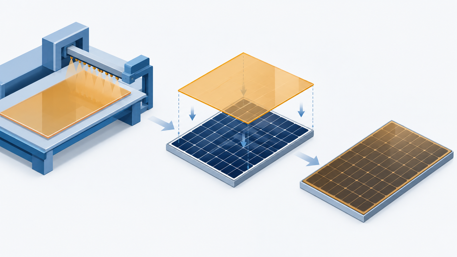
Tandem PV is a California company co-founded in 2016 by Colin Bailie, the researcher who made the first perovskite-silicon tandem cell at Stanford University. What sets it apart is its panel structure: rather than a monolithic design that deposits perovskite directly on a silicon cell, it stacks layers made separately. In April 2026 it opened a commercial demonstration factory in Fremont, California, with about 40 MW a year of capacity, and it aims to sell its first commercial panels during 2026 and reach high-volume manufacturing in 2028. In August of the same year it was selected by ARPA-E, part of the U.S. Department of Energy (DOE), for about US$7.7 million in support. Tandem PV is privately held, so this profile uses only the company's own announcements and U.S. government publications to sort out what is settled and what cannot yet be seen.
- Tandem PV in 30 seconds, and where it stands in perovskite solar cells
- The logo and how the name is written
- Where the company sits in the perovskite solar landscape
- Scale (revenue is not disclosed, so we look at funding and the factory)
- Resources committed to perovskites
- Track record so far
- Plans ahead
- What the company is aiming for in perovskite solar cells
- Partnership map
- Technology, products and services
- The risks this company carries
- Glossary, references and claim-to-source audit
1. Tandem PV in 30 seconds, and where it stands in perovskite solar cells
California, U.S.Announcements up to 2025 gave San Jose
Founded 2016No financial statements published
start-upMakes its panels in house
(stacked)The company says explicitly that it is not monolithic
about 40 MW a yearCommercial demonstration factory opened April 2026
Companies working on perovskite solar cells fall into three broad groups: established PV makers, perovskite start-ups, and newcomers from materials, chemicals and electronics. Tandem PV is a perovskite start-up, and one that makes and sells panels itself. On top of that, the company says in its FAQ that its stacked design differs from most competitors, which deposit perovskite directly onto silicon cells to make monolithic tandem cells Sourced. Among U.S. perovskite start-ups, it sits between the companies that chose two-terminal monolithic cells and the one that sells only a glass component, having chosen to make the layers separately, stack them and sell a finished panel.
2. The logo and how the name is written

The Tandem PV logo is a trademark of the company. We have not recreated it with generated imagery;
the image shown in the header of the official website was taken and is placed here as img/tandem_pv_logo.png.
A note on names: the legal entity is Tandem PV, Inc. The company explains in its FAQ that "PV" stands for photovoltaic. Because "tandem" is also the generic name of the technology, this article always writes "Tandem PV" when referring to the company and "tandem" when referring to the technology.
Official site: https://www.tandempv.com/3. Where the company sits in the perovskite solar landscape
In terms of product format, Tandem PV makes a tandem with silicon, but not a two-terminal monolithic device in which the top and bottom are connected in series within a single cell. The company describes its panels as stacking conventional silicon cells with thin-film perovskite material Sourced. How the top and bottom layers are connected electrically (taken out separately as four terminals, or wired together inside the panel), however, has not been disclosed Not yet confirmed. The difference between two-terminal and stacked designs is covered in our explainer on silicon–perovskite tandems.
4. Scale (revenue is not disclosed, so we look at funding and the factory)
Tandem PV is privately held and does not publish revenue, profit or loss, cash on hand or headcount Not yet confirmed. As of April 2026 it said it "plans to sell its first commercial panels in 2026", and it has not said whether it has any revenue yet. Instead we look at the cumulative funding figure the company updates at the end of each release, and at the size of its factory.
| When | What the company announced | Amount | Where stated |
|---|---|---|---|
| March 2025 | Series A and debt, led by Eclipse, with participation from Constellation Energy, Planetary Technologies, Uncorrelated Ventures, Trellis Climate, Tom Werner (former CEO of SunPower), Stifel Bank, CSC Leasing and others | US$50 million | Official release |
| March to June 2025 | Cumulative venture capital, debt and government funding (company boilerplate at the end of releases) | US$83 million | Official releases |
| July 2025 to June 2026 | Same as above | US$87 million | Official releases |
| August 2026 | Same as above. 8090 Industries added to the list of investors | US$100 million | Official release |
| Date not stated | Cumulative public funding (15 grants from DOE, NSF, the California Energy Commission and others) | US$13 million | Official FAQ |
The cumulative figure at the end of the releases was US$87 million in the announcement of 1 June 2026 and US$100 million in that of 3 August. That is an increase of about US$13 million in two months Our calculation. 8090 Industries appears among the investors over the same period, but no announcement explaining the breakdown of the increase (new equity or debt) could be found Not yet confirmed. The ARPA-E award of about US$7.7 million, whose selection was announced on 25 August, came after the US$100 million announcement.
The other yardstick of scale is the factory. The company says its Fremont commercial demonstration site covers 65,000 square feet (about 6,000 m²), its line has approximately 40 MW of annual nameplate capacity, and its panels are roughly 60 times larger than its R&D-scale devices Sourced. The conversion from square feet uses 1 sq ft = 0.0929 m² Our calculation.
5. Resources committed to perovskites
Perovskite-silicon tandem panels are Tandem PV's only business, so almost everything the company spends goes into perovskites. The amounts are not disclosed, but the published material shows concretely what the money is going into.
| Resource | Details | Category |
|---|---|---|
| People (technology) | Co-founder and CTO Colin Bailie (developed the first perovskite-silicon tandem cell at Stanford University). Co-founder Chris Eberspacher (led solar technology development at Hanwha Solar, SoloPower, Nanosolar and Applied Materials) | Sourced |
| People (manufacturing and quality) | VP of Manufacturing Clemens Hofbauer (formerly plant manager of SunPower's module factory in Oregon; joined May 2025), VP of Operations Frank Blohm (joined June 2025) and VP of Quality Robert Meagley (formerly of the DOE Solar Energy Technologies Office; joined November 2025) | Sourced |
| People (management and board) | CEO Scott Wharton (formerly head of Logitech for Business). In June 2026 former U.S. Energy Secretary Jennifer Granholm joined the board | Sourced |
| People (headcount) | Number of employees | Not disclosed |
| Money (funding) | US$100 million in total (venture capital, debt and government funding; August 2026), including US$50 million in Series A and debt (March 2025) | Sourced |
| Money (factory) | The Fremont commercial demonstration factory (about 40 MW). Investment not disclosed | Sourced / not disclosed |
| Acquisitions | Acquired nexTC Corporation (Oregon; solution-based transparent oxide coatings) in August 2026. Its technology, intellectual property and founder join the company. Price not disclosed | Sourced |
| Public funding | DOE Solar Energy Technologies Office project "STACKED", US$4.7 million (selected May 2024); California Energy Commission, US$4 million (July 2025); ARPA-E "SCALEUP Ready", about US$7.7 million (selected August 2026). The official FAQ puts public funding at US$13 million across 15 grants | Sourced |
| Universities and research institutes | Founded through Activate, a DOE start-up programme (Cyclotron Road at Lawrence Berkeley National Laboratory). The website lists partnerships with DOE, NSF, the CEC and that laboratory. With CEC funding, it will work with independent labs and technical institutions on third-party testing | Sourced |
The description of Tandem PV's project "STACKED", selected by DOE in 2024, states that "Ultraviolet (UV) light from the sun can cause significant damage to perovskite PV devices, but current simulated outdoor durability testing does not adequately account for its effects" Sourced. The project aims to engineer UV hardness into critical layers of the device, such as the hole transport layer, while also improving durability at high temperature. Perovskite degradation often happens not only in the absorber itself but in the charge transport layers on either side and their interfaces, and the company's 2026 acquisition of nexTC, a maker of transparent oxide coatings, can be read as an extension of the same concern: controlling these sandwiching layers in house Inference.
The nexTC acquisition release explains that these ultrathin oxide layers "modify charge transport while allowing sunlight to reach the silicon cell below", and that "their performance is important to module efficiency, durability and manufacturability" Sourced. For encapsulation and layer stacks, see also our explainer on encapsulation and barrier layers.
6. Track record so far
| When | What happened | What it means |
|---|---|---|
| Before founding | As a PhD student at Stanford University, Bailie develops the first perovskite-silicon tandem cell | Where the technology comes from |
| 2016 | Bailie and Eberspacher found the company under a DOE support programme (Cyclotron Road / Activate) | Born out of a national laboratory's start-up programme |
| May 2024 | DOE selects STACKED (UV-hard hole transport layers) for US$4.7 million (principal investigator: Bailie) | Public funding for durability research |
| March 2025 | US$50 million in Series A and debt (led by Eclipse). Announces it will build a commercial-scale manufacturing facility in the U.S. Panel efficiency 28% | Money for the factory secured |
| May to June 2025 | VP of Manufacturing and VP of Operations appointed | Building the team for volume production |
| July 2025 | US$4 million from the California Energy Commission, to fund third-party testing of performance and durability by independent institutions | Money for external validation |
| November 2025 | VP of Quality (formerly of DOE) appointed. Announces panel efficiency of 29% | Transition from prototypes to commercial scale |
| April 2026 | Opens a commercial demonstration factory in Fremont (about 40 MW). 29.7% efficiency in internal testing; less than 1% average annual power loss in accelerated lifetime testing (about a tenfold improvement on a year earlier) | From R&D to the stage of validating volume production |
| June 2026 | Former U.S. Energy Secretary Granholm joins the board. Announces that its latest mini-modules reached 30.4% in internal testing and are going through external certification | Efficiency still measured in house |
| 3 August 2026 | Acquires nexTC, bringing in transparent oxide coating technology and intellectual property | Bringing a core process in house |
| 25 August 2026 | Selected for ARPA-E SCALEUP Ready (about US$7.7 million; project name "TANDEM") | Public funding backs the move to large-scale commercial production |
7. Plans ahead
producers (IPPs)The company says it is focusing on utility-scale solar
In its April 2026 release on the factory opening, the company wrote that shipments were planned "to support customer validation trials later this year", that it "plans to sell its first commercial panels in 2026" and that it is "targeting high-volume manufacturing in 2028" Sourced. The official website says that besides selling finished panels for utility-scale projects, it will also work with solar manufacturers that want to build a perovskite layer into their existing silicon panel designs Sourced.
None of the following appears in the company's published material Not yet confirmed.
The location, capacity and investment of the factory for high-volume manufacturing in 2028 / customer names and shipment volumes / the selling price of the panels / the names of solar manufacturers it may partner with / the price paid for nexTC / the result of external certification and the name of the certifying body for 30.4% / the electrical connection between the top and bottom layers. Figures of the "Tandem PV to build an X GW factory" kind exist in press reports, and this article does not use them.
8. What the company is aiming for in perovskite solar cells
This section includes things the company does not say directly. We set them out as inferences within what the primary sources support, with the evidence for each.
| What the evidence suggests | Primary information it rests on | Category |
|---|---|---|
| It chose a structure that puts manufacturability and yield ahead of the monolithic approach | The FAQ stresses its stacked design as what distinguishes it from competitors' monolithic designs, and likens perovskite manufacturing to making window glass or televisions, coating a single surface at low temperature | Inference |
| For now it is selling "the combination of efficiency and durability" rather than efficiency alone | Since November 2025 the boilerplate at the end of its releases has claimed "the market's best combination of efficiency and durability", and it presents the sub-1%-a-year degradation in accelerated testing alongside efficiency | Inference |
| It is bringing core processes in house so that it can optimise them directly on the line | In the nexTC acquisition release, the CEO said it "gives us greater control over a core part of the manufacturing process and allows us to optimize it directly on our production line as we scale" | Sourced |
| It is keeping both finished-panel sales and technology partnerships open as options | The official website lists, alongside IPPs, solar manufacturers that want to build a perovskite layer into existing silicon panels as customers | Inference |
| It places weight on U.S. manufacturing and policy support | It has brought a former U.S. Energy Secretary onto its board and continues to receive DOE, ARPA-E and California funding. Its releases consistently speak of bringing back U.S. leadership in solar manufacturing | Inference |
The answer on efficiency and durability in the official FAQ still says that its newest, highest-performing panels are under test and that independent, industry-standard validation of efficiency and durability was expected during 2024 Sourced. Yet even in its June 2026 release, the 30.4% achieved by its latest mini-modules was "in internal testing" and "now advancing through external certification" Sourced. From this we read that third-party certification of its efficiency is running later than the company originally expected Not yet confirmed. That the company says explicitly it will use the California funding for "third-party testing and validation" also shows that external validation is the next hurdle. It is possible, however, that the FAQ has simply not been updated, and the company has not explained any delay. This remains our interpretation.
9. Partnership map
10. Technology, products and services
| Item | What the company has published |
|---|---|
| Panel structure | A tandem panel that stacks conventional silicon cells with thin-film perovskite. Not a monolithic design in which perovskite is deposited directly on the silicon cell |
| Perovskite layer | About 1 micrometre thick (about one two-hundredth of a 100 to 150 micrometre silicon wafer). A few grams of material in a whole panel |
| Manufacturing process | Described as close to making window glass or televisions: a single surface coated at low temperature. Process temperature about 150 °C (silicon is heated to about 1,500 °C), with about a tenth of the energy needed to manufacture |
| Lead content | Claims about a fifteenth of that in conventional silicon panels. Says it holds patents on recycling lead |
| Product dimensions | Standard-size panels that integrate into existing utility-scale infrastructure |
| Warranty | Plans to offer industry-standard warranties |
| Efficiency and durability claim | Cell or module, and area | Certified? |
|---|---|---|
| Panel efficiency of 28% (March and July 2025) and 29% (November 2025) | Panel. Area not stated | Company-reported |
| 29.7% (April 2026, as an R&D result) | Not stated (described as being translated into production panels) | Company-reported (in-house measurement) |
| 30.4% for its latest-generation mini-modules (June 2026) | Mini-module. Area not stated | In-house measurement. The company says it is going through external certification |
| Less than 1% average annual power loss in accelerated lifetime testing | Latest-generation panels | Company-reported (accelerated test conditions not disclosed) |
| Projected to surpass 30% by late 2025 (March 2025) | Panel | A projection |
| NREL's Best Research-Cell Efficiency chart and Champion Module Efficiencies chart (both revised 17 July 2026) | - | Tandem PV's name does not appear |
The company writes that its panels "currently achieve 29% efficiency, making them 30% more powerful than the average silicon solar panel" (November 2025), and that 30% efficiency "translates into roughly 40% more power in the same form factor" (official website). Working backwards, the "average silicon panel" used for comparison is assumed to be 29 ÷ 1.3 ≈ 22.3% efficient in the first case and 30 ÷ 1.4 ≈ 21.4% in the second Our calculation. The comparison baseline shifts slightly from one announcement to the next, which is worth keeping in mind when reading the numbers. How to read efficiency figures is covered in our explainer on conversion efficiency and evaluation metrics.
A monolithic (two-terminal) tandem deposits perovskite directly on the textured surface of a silicon cell, so the silicon processes and the perovskite processes become entangled on a single wafer. A defect on one side takes the other down with it, and the currents in the top and bottom must also be matched. A stacked design makes the perovskite separately on a flat substrate and combines it with the silicon afterwards, so, as Tandem PV's FAQ says, a single surface coated at low temperature is enough, and off-the-shelf silicon cells can be used Inference.
In exchange, the extra layer adds optical losses in the transparent electrodes and substrate, and the parts count rises; that is the general trade-off Inference. Tandem PV's acquisition of nexTC's transparent oxide coatings can be read as a response to exactly this: the layer that carries current while letting light through governs the efficiency and durability of a stacked design. That the acquisition release describes this layer as "allowing sunlight to reach the silicon cell below" is consistent with this reading Sourced.
11. The risks this company carries
| Risk | Details | Category |
|---|---|---|
| Finances cannot be seen | Privately held, with no published revenue, profit or loss, or cash. The breakdown of the increase in cumulative funding (about US$13 million between June and August 2026) has not been explained | Not yet confirmed |
| Efficiency not certified by third parties | The 30.4% is an in-house measurement going through external certification. Not listed in NREL's efficiency charts either | Sourced |
| Delayed validation | The FAQ says independent industry-standard validation was expected during 2024, yet certification was still in progress as of June 2026 | Sourced |
| Distance from demonstration plant to volume production | The current factory is about 40 MW. The location, size and funding of the factory for high-volume manufacturing in 2028 have not been disclosed | Sourced |
| Choosing a structure that differs from the mainstream | The company itself says most competitors are monolithic. A higher parts count could work against it on cost | Inference |
| Inconsistent published figures | The DOE selection list gives DOE's share of STACKED as US$4.7 million, whereas a company release says it "was awarded $5.2 million from the U.S. Department of Energy" in late 2024. The FAQ counts 15 public grants and the home page 16, and cumulative funding moves from US$83 million to US$87 million to US$100 million across releases | Sourced |
12. Glossary
- Perovskite solar cell
- A solar cell whose light-absorbing layer is a metal halide material with the perovskite crystal structure. It can be made thin and absorbs light strongly.
- Monolithic tandem
- A cell in which perovskite is deposited directly on a single silicon cell and the two are integrated in series; also called a two-terminal tandem.
- Stacked design
- An approach in which the perovskite and the silicon are made separately and then stacked. This is what Tandem PV calls its own structure.
- Hole transport layer
- A layer that carries the positive charges (holes) created by light to the electrode. It touches the perovskite layer and is a common starting point for degradation.
- Transparent oxide coating
- A thin oxide film that carries current while letting light through. In tandems it is used at key points linking the top layer and the silicon below.
- Accelerated lifetime testing
- Testing under harsh conditions such as high temperature, high humidity and strong light to speed up degradation and estimate long-term lifetime in a short time.
- IPP
- Independent power producer: a company that builds power plants and sells the electricity.
- ARPA-E
- The Advanced Research Projects Agency-Energy of the U.S. Department of Energy, which funds innovative energy technologies that are not yet ready for commercial use.
13. References
- Tandem PV, Inc. Official website, home page. 30% efficiency, roughly 40% more power, less than 1% annual degradation in accelerated tests, US$87 million raised and 16 government grants, IPPs as the first customers, the policy of working with solar manufacturers, the company name (copyright notice), and source of the logo image. https://www.tandempv.com/
- Tandem PV, Inc. Official website, "About". Founding in 2016, backgrounds of the founders and management, US$100 million in funding, and partnerships with DOE, NSF, the CEC and Lawrence Berkeley National Laboratory. https://www.tandempv.com/about
- Tandem PV, Inc. Official website, "FAQ". The difference between stacked and monolithic designs, 29% efficiency, independent validation expected in 2024, a process at about 150 °C, perovskite layer thickness, lead content, first customers, warranties, what the name stands for, US$13 million in public funding across 15 grants, and US$87 million raised. https://www.tandempv.com/faq
- Tandem PV, Inc. Official website, "Technology". The thinness of the perovskite layer and a design aiming at 30% or more. https://www.tandempv.com/technology
- Tandem PV Press release, "Tandem PV Raises $50M to Take Back U.S. Leadership With New Perovskite Solar Manufacturing" (4 March 2025). US$50 million in Series A and debt, led by Eclipse, and the participants; building a manufacturing facility in the U.S.; 28% efficiency and a projection of above 30% by late 2025; US$83 million in total. https://www.prnewswire.com/news-releases/tandem-pv-raises-50m-to-take-back-us-leadership-with-new-perovskite-solar-manufacturing-302390991.html
- Tandem PV Press release, "Tandem PV Appoints Clemens Hofbauer as VP of Manufacturing to Scale U.S. Production of High-Efficiency Perovskite Solar Panels" (12 May 2025). Appointment and background of the VP of Manufacturing. https://www.tandempv.com/news/tandem-pv-appoints-clemens-hofbauer-as-vp-of-manufacturing-to-scale-u.s.-production-of-high-efficiency-perovskite-solar-panels
- Tandem PV Press release, "Tandem PV Names Frank Blohm as Vice President of Operations to Drive Scale and Strengthen U.S. Solar Leadership" (17 June 2025). Appointment of the VP of Operations; US$83 million in total. https://www.tandempv.com/news/tandem-pv-names-frank-blohm-as-vice-president-of-operations-to-drive-scale-and-strengthen-u.s.-solar-leadership
- Tandem PV Press release, "Tandem PV Awarded $4M California Energy Commission Grant to Accelerate Commercial Readiness of Next-Gen Solar Panels" (17 July 2025). The CEC's US$4 million, third-party testing by independent institutions, 28% efficiency, the statement of US$5.2 million from DOE in late 2024, and US$87 million in total. https://www.tandempv.com/news/tandem-pv-awarded-%244m-california-energy-commission-grant-to-accelerate-commercial-readiness-of-next-gen-solar-panels
- Tandem PV Press release, "Tandem PV Strengthens Executive Team With Appointment of Leading Materials Scientist Dr. Robert Meagley as Vice President of Quality" (18 November 2025). Appointment and background of the VP of Quality; 29% efficiency. https://www.tandempv.com/news/tandem-pv-strengthens-executive-team-with-appointment-of-leading-materials-scientist-dr.-robert-meagley-as-vice-president-of-quality
- Tandem PV Press release, "Tandem PV Opens California Factory for Next-Generation Solar Manufacturing" (20 April 2026). The Fremont commercial demonstration factory (65,000 sq ft, about 40 MW, panels about 60 times the size of R&D devices), 29.7% in internal testing, less than 1% annual degradation, first commercial sales in 2026 and high-volume manufacturing in 2028. https://www.tandempv.com/news/tandem-pv-opens-california-factory-for-next-generation-solar-manufacturing
- Tandem PV Press release, "Former U.S. Energy Secretary Jennifer Granholm Joins Tandem PV Board of Directors" (1 June 2026). Board appointment, 30.4% for mini-modules (internal testing, going through external certification), and US$87 million in total. https://www.tandempv.com/news/former-u.s.-energy-secretary-jennifer-granholm-joins-tandem-pv-board-of-directors
- Tandem PV Press release, "Tandem PV Acquires nexTC to Bring Critical Coating Technology In-House" (3 August 2026). Acquisition of nexTC, the role of transparent oxide coatings, the CEO's comments, US$100 million in total and 8090 Industries. https://www.tandempv.com/news/tandem-pv-acquires-nextc-to-bring-critical-coating-technology-in-house
- Tandem PV Press release, "Tandem PV Selected for ARPA-E SCALEUP Ready Award to Accelerate American Solar Manufacturing" (25 August 2026). About US$7.7 million; project name "TANDEM". https://www.tandempv.com/news/tandem-pv-selected-for-arpa-e-scaleup-ready-award-to-accelerate-american-solar-manufacturing
- U.S. Department of Energy (DOE) Advancing U.S. Thin-Film Solar Photovoltaics Funding Program (selections announced 16 May 2024). Tandem PV's project "STACKED: Stability and Characterization of Hole-Transporting Layers Key to Enabling Outdoor Durability", DOE award of US$4.7 million, cost share of US$2 million, principal investigator Colin Bailie, and development of UV-hard hole transport layers. https://www.energy.gov/cmei/systems/advancing-us-thin-film-solar-photovoltaics-funding-program
- Tandem PV, Inc. Official website, "Investors". US$100 million in funding and the claim of up to 50% higher efficiency. https://www.tandempv.com/investors
- NREL (now the National Laboratory of the Rockies) Best Research-Cell Efficiency Chart (revised 17 July 2026). Used to confirm that no Tandem PV record is listed. https://www.nlr.gov/docs/libraries/pv/best-research-cell-efficiencies.pdf
- NREL (now the National Laboratory of the Rockies) Champion Module Efficiencies chart (revised 17 July 2026). Used to confirm that no Tandem PV record is listed. https://www.nlr.gov/docs/libraries/pv/champion-module-chart.pdf
14. Claim-to-source audit
| Claim in the article | Category | Source |
|---|---|---|
| The legal name is Tandem PV, Inc.; headquarters (Fremont); the official logo | Sourced | Reference 1 https://www.tandempv.com/ |
| Founding in 2016, the backgrounds of the two founders, founding through Cyclotron Road / Activate, and the management's backgrounds | Sourced | References 2 and 3 https://www.tandempv.com/about |
| A stacked, not monolithic, design; the low-temperature coating process; about 150 °C; layer thickness; lead content; independent validation expected in 2024; US$13 million across 15 public grants; what the name stands for | Sourced | Reference 3 https://www.tandempv.com/faq |
| US$50 million in Series A and debt, led by Eclipse, and the participants; building a U.S. manufacturing facility; 28% efficiency; US$83 million in total (March 2025) | Sourced | Reference 5 https://www.prnewswire.com/news-releases/tandem-pv-raises-50m-to-take-back-us-leadership-with-new-perovskite-solar-manufacturing-302390991.html |
| Appointment of the VP of Manufacturing and VP of Operations (May and June 2025) | Sourced | References 6 and 7 https://www.tandempv.com/news/tandem-pv-names-frank-blohm-as-vice-president-of-operations-to-drive-scale-and-strengthen-u.s.-solar-leadership |
| The CEC's US$4 million and third-party testing; the company's statement of US$5.2 million from DOE in late 2024 | Sourced | Reference 8 https://www.tandempv.com/news/tandem-pv-awarded-%244m-california-energy-commission-grant-to-accelerate-commercial-readiness-of-next-gen-solar-panels |
| Appointment and background of the VP of Quality; 29% efficiency (November 2025) | Sourced | Reference 9 https://www.tandempv.com/news/tandem-pv-strengthens-executive-team-with-appointment-of-leading-materials-scientist-dr.-robert-meagley-as-vice-president-of-quality |
| Opening and size of the Fremont factory, 29.7% (internal testing), less than 1% annual degradation, commercial sales in 2026 and high-volume manufacturing in 2028 | Sourced | Reference 10 https://www.tandempv.com/news/tandem-pv-opens-california-factory-for-next-generation-solar-manufacturing |
| Granholm's board appointment; 30.4% for mini-modules in internal testing, going through external certification; US$87 million in total | Sourced | Reference 11 https://www.tandempv.com/news/former-u.s.-energy-secretary-jennifer-granholm-joins-tandem-pv-board-of-directors |
| Acquisition of nexTC, the role of transparent oxide coatings, the CEO's comments, US$100 million in total and 8090 Industries | Sourced | Reference 12 https://www.tandempv.com/news/tandem-pv-acquires-nextc-to-bring-critical-coating-technology-in-house |
| Selection for ARPA-E SCALEUP Ready (about US$7.7 million, TANDEM) | Sourced | Reference 13 https://www.tandempv.com/news/tandem-pv-selected-for-arpa-e-scaleup-ready-award-to-accelerate-american-solar-manufacturing |
| DOE's STACKED (US$4.7 million, US$2 million cost share, UV-hard hole transport layers, selected May 2024) | Sourced | Reference 14 https://www.energy.gov/cmei/systems/advancing-us-thin-film-solar-photovoltaics-funding-program |
| 30% efficiency and roughly 40% more power, 16 government grants, IPPs as the first customers, and the policy of partnering with solar manufacturers | Sourced | Reference 1 https://www.tandempv.com/ |
| A design aiming at 30% or more, US$100 million in funding, and the claim of up to 50% higher efficiency | Sourced | References 4 and 15 https://www.tandempv.com/investors |
| Tandem PV's name does not appear in NREL's research-cell or champion module efficiency charts | Sourced | References 16 and 17 https://www.nlr.gov/docs/libraries/pv/best-research-cell-efficiencies.pdf |
| Cumulative funding rose by about US$13 million between June and August 2026 | Our calculation | This article's calculation from the difference between the cumulative figures in references 11 and 12 |
| Factory floor area converted to about 6,000 m² | Our calculation | This article's calculation: 65,000 sq ft in reference 10 multiplied by 0.0929 |
| The comparison "average silicon panel" is assumed to be 22.3% and 21.4% efficient | Our calculation | Worked back in this article from the figures in references 9 and 1 |
| The three types of perovskite solar company | Our calculation | This article's own classification. Examples drawn from the companies covered in this series |
| Revenue, profit or loss, cash, headcount and factory investment | Not yet confirmed | Not published, as the company is private. This article does not estimate them |
| Location, capacity and investment of the volume factory; customer names and volumes; price; partner names; nexTC's price; the certification result for 30.4%; the layer connection; the breakdown of the increase in cumulative funding | Not yet confirmed | None stated in the company's published material. This article does not use press-based figures |
| The reading that it is selling the combination of efficiency and durability for now | Inference | This article's interpretation of the company boilerplate and presentation of figures in references 9 to 13 |
| The reading that it chose a structure favouring manufacturability and yield over the monolithic approach | Inference | This article's interpretation of statements in reference 3 |
| The reading that it is keeping both finished-panel sales and technology partnerships open | Inference | This article's interpretation of the customer description in reference 1 |
| The reading that it places weight on U.S. manufacturing and policy support | Inference | This article's interpretation of references 8, 11, 13 and 14 |
| The reading that third-party efficiency certification is running later than originally expected | Inference | This article's interpretation from comparing references 3 and 11. The FAQ may simply not have been updated |
| The reading that the nexTC acquisition reflects the same concern with charge transport layers and interfaces, and the trade-offs of a stacked design | Inference | This article's commentary based on references 12 and 14 and general understanding of device structures |
| The cost risk of choosing a structure that differs from the mainstream | Inference | This article's interpretation of statements in reference 3 |
Last updated 25 September 2026 / Troy Technical
Every figure in this article comes from Tandem PV's official press releases and website, and from publications of the U.S. Department of Energy and NREL. No research-firm estimates or press-based figures have been used (nor have the research-firm market forecasts quoted on the company's technology page). Efficiency and durability figures not confirmed by a testing body are labelled "company-reported" or "in-house measurement". Passages marked "Inference" are this article's interpretation of the primary sources, not statements made by the company.