COMPANY PROFILE / OPTICAL COMMUNICATIONS & PHOTONICS
GlobalFoundries
A foundry that is buying, bundling and growing optical manufacturing in the United States
GlobalFoundries (GF) is a U.S. foundry that has stepped back from the race to the most advanced process nodes. In less than a year from November 2025, that company acquired AMF, a Singapore foundry dedicated to silicon photonics, for US$453 million, bought a designer of optical communications chips, launched "SCALE" for co-packaged optics (CPO), and signed a letter of intent with the U.S. Department of Commerce for a US$300 million R&D award. It has also teamed up with SMART Photonics of the Netherlands to offer a foundry service that mounts indium phosphide (InP) lasers, the light source, onto its chips. This profile confines the company-wide figures to a single table and sets out what GF has bought for optics, whom it works with and how much it can make, using only its U.S. SEC filings and official announcements by GF and its partners.
- GlobalFoundries in 30 seconds, and where it stands in optical communications and photonics
- The logo and how the name is written
- Where the company sits in optical communications and photonics
- Scale (the company as a whole, in brief)
- Resources committed to optical communications and photonics
- Track record so far
- Plans ahead
- What the company is aiming for in optical communications and photonics
- Partnership map
- Technologies, products and services
- The risks this company carries
- Glossary, references and claim-to-source audit
1. GlobalFoundries in 30 seconds, and where it stands in optical communications and photonics
New York, U.S.400 Stonebreak Road Extension
US$453 millionA Singapore silicon photonics pure-play. November 2025
(letter of intent stage)U.S. Department of Commerce CHIPS R&D Office. July 2026
Companies involved in optical communications fall into three broad types: optical components & modules, chips & foundries, and network systems & carriers. GF belongs to chips & foundries and is the party that manufactures, under contract, photonic chips (PICs) designed by its customers Sourced.
What sets GF apart is that it is trying to assemble, across its own group of fabs, the parts needed to send and receive light: not only photonic chips, but also the high-speed analogue circuits (SiGe) that turn optical signals back into electrical ones, packaging, and, since September 2026, a process that mounts light sources (InP lasers), which cannot be made in silicon. The 20-F positions silicon photonics as one of six differentiated product families, and in the August 2026 earnings release the CEO named "Optical Networking within the AI data center" as one of the company's strategic growth drivers.
2. The logo and how the name is written

The GlobalFoundries logo is a trademark of the company. We have not recreated it with generated imagery;
the SVG logo embedded in the official website was extracted as is and placed here as img/globalfoundries_logo.svg.
A note on names: the name in statutory filings is GLOBALFOUNDRIES Inc. in capitals, the logo and general usage write GlobalFoundries, and the company abbreviates itself as GF. This article writes "GlobalFoundries (GF)" at first mention and GF thereafter. Advanced Micro Foundry (AMF), which GF acquired, has an abbreviation similar to AMD's but is an unrelated company.
Official site: https://gf.com/3. Where the company sits in optical communications and photonics
The middle box in Fig. 1 is described as "owns the switches and GPUs", but that trait applies to chip companies with their own products, such as NVIDIA and Broadcom, not to GF. GF owns no end products; it is in the position of taking manufacturing orders from companies that do, and from optical module makers Not yet confirmed. In exchange, GF covers a broad range of optics: its official technology page says it supports every form factor, pluggable optical transceivers (including long-haul coherent optics), LPO, NPO and CPO Sourced. The differences between these approaches are covered in our explainers on optical transceivers, on NPO and LPO, and on co-packaged optics.
4. Scale (the company as a whole, in brief)
The company as a whole is not the subject here, so we note only its size and the revenue of the end market that includes optics Sourced.
| Measure (US$ million) | FY2023 | FY2024 | FY2025 |
|---|---|---|---|
| Revenue | 7,392 | 6,750 | 6,791 |
| of which communications infrastructure and data center | 863 (12%) | 577 (9%) | 745 (11%) |
| R&D expense | - | 496 (7.3% of revenue) | 518 (7.6% of revenue) |
| Employees (31 December) | - | - | About 14,000 (about 1,600 in R&D) |
A dash means the relevant passage of the FY2025 20-F used for this article gives no figure.
Besides optics, "communications infrastructure and data center" includes wireless base stations (5G and 6G), satellite communications and timing ICs. The 20-F attributes this segment's 29.1% growth in 2025 to "growth in silicon photonics optical networking and satellite communications", but does not disclose revenue for silicon photonics alone Not yet confirmed. AMF, the acquired company, is stated to account for less than 1% of consolidated revenue and about 1% of total assets in 2025 (because the deal closed in November, only about a month and a half was consolidated). Figures of the "GF's silicon photonics revenue will double in 2026" kind come from press reports or research firms, and this article does not use them.
5. Resources committed to optical communications and photonics
As a matter of method, we checked four things: people, money, external investment or acquisitions, and universities or public funding. GF provides concrete information on all four.
| Resource | Details | Category |
|---|---|---|
| People (dedicated organisation) | Official announcements feature a senior vice president responsible for the "Photonics & RF businesses" and a senior fellow in the silicon photonics business, showing that there is a business organisation responsible for optics. Dedicated optics headcount is not disclosed. The company has about 1,600 R&D staff in total | Sourced |
| People (engineers gained through acquisitions) | AMF's people (more than 15 years of manufacturing experience) and InfiniLink's design engineers in Egypt. InfiniLink is described as strong in designing SerDes, chipsets for optical transceivers and monolithic silicon photonics | Sourced |
| Money (acquisitions) | AMF: US$453 million (cash) / InfiniLink: US$48 million. Both November 2025 | Sourced |
| Money (R&D and facilities) | Company-wide R&D expense was US$518 million (2025). The optics share and optics-related capital spending are not disclosed | Not disclosed |
| Public funding | In July 2026 it signed a letter of intent (LOI) under which the Department of Commerce's CHIPS R&D Office would award US$300 million. Targets include novel optical materials, wafer technology and advanced packaging including 3D hybrid bonding. Under a separate agreement the Department of Commerce receives about 1% of GF's shares | Sourced (award not yet final) |
| Research institutes | Plans a silicon photonics centre of excellence (CoE) in Singapore, to research next-generation materials for 400 Gbps with the government research agency A*STAR | Sourced (plan) |
| Sites | Makes 300 mm and 200 mm silicon photonics in Malta, New York, and in Singapore. Has an "Advanced Photonics & Packaging Center" in Malta and plans to onshore packaging to the United States. SiGe is made in Burlington, Vermont | Sourced |
The CHIPS award letter of intent lists novel optical materials first among its targets Sourced. Silicon is an excellent material for waveguides that carry light, but its electro-optic effect, the ability to modulate light electrically, is weak, and it cannot emit light. So as per-lane speeds move from 200G to 400G, companies are researching ways to combine silicon waveguides with materials that have a stronger electro-optic effect (see our explainers on optical modulation and modulation formats, and on thin-film lithium niobate). GF has not disclosed which material it will use Not yet confirmed. But the research planned with A*STAR in Singapore is also on "next-generation materials for 400 Gbps", and the wording of both announcements suggests that the company sees replacing materials as the focus of the next generation.
6. Track record so far
| When | What happened | What it means |
|---|---|---|
| Up to 2025 | GF describes itself as having more than a decade of technology and manufacturing experience in silicon photonics. Offers first-generation (up to 100G per wavelength) and second-generation (up to 200G per wavelength) processes | The foundation for today's pluggable transceivers |
| More than ten years ago | Collaboration with Marvell begins (the September 2026 announcement describes more than a decade of collaboration). GF has manufactured advanced SiGe for over a decade | A long trading relationship on the "electrical side" of optics as well |
| 14 November 2025 | Acquires InfiniLink for US$48 million, a designer of optical data connectivity chips for hyperscale data centres | Gains in-house photonic chip design capability |
| November 2025 | Acquires AMF for US$453 million. GF claims it has become the largest pure-play silicon photonics foundry by revenue | Adds a 200 mm line in Singapore to its U.S. capacity. The 20-F itself gives two different completion dates, 14 November and 18 November |
| Full year 2025 | Communications infrastructure and data center revenue rises 29.1% year on year to US$745 million, with silicon photonics optical networking cited as a reason | Optics starts to show up in the numbers (no standalone figure disclosed) |
| March 2026 | At OFC 2026, demonstrates wafer-level detachable fibre connections with SENKO and shows a suite of CPO technologies with Corning and EXFO. Siluxtek announces it will manufacture 200G-per-lane silicon photonics receiver chips at GF | Tackles a volume-production bottleneck for CPO: how to attach fibre and how to test it |
| 4 May 2026 | Announces SCALE, an optical module technology for CPO, which it claims is the first platform to exceed OCI MSA specifications | Now has a product it can present to customers in optical engine form |
| 29 July 2026 | Signs a letter of intent for a US$300 million CHIPS R&D award with the Department of Commerce. Executives from AMD, Broadcom, Cisco, Corning, Lumentum, Marvell, Meta, Microsoft, NVIDIA and Qualcomm contribute supporting comments | The government is now backing volume optical production in the United States |
| 5 August 2026 | In second-quarter results, the CEO names "Optical Networking within the AI data center" as one of the strategic growth drivers | Publicly declared a management priority |
| 17 September 2026 | Expands its multi-year agreement with Marvell. Increases SiGe capacity at the Burlington fab to supply optical connectivity for pluggables, NPO and CPO. Current technology supports 200G per lane | Captures a large customer's demand for the electrical-side parts of optics |
| 21 September 2026 | Announces with SMART Photonics an open-access foundry service combining silicon and InP. SMART Photonics' lasers and SOAs are flip-chip mounted in cavities etched into GF's silicon. General availability planned for the second half of 2027 | Opens a route to bring light sources, which silicon cannot make, into its own process |
7. Plans ahead
a path to 400G per wavelengthEarly access available. Volume timing not disclosed
5x power efficiencyVersus the current generation. Targets stated in the CHIPS announcement
The official technology page also mentions support for on-chip lasers (in development) and plans to onshore packaging to the Advanced Photonics & Packaging Center in Malta Sourced. The CHIPS award letter of intent states its purpose as creating a path to volume production of NPO and CPO in the United States, using existing facilities in Malta and Burlington.
None of the following appears in GF's official materials or SEC filings Not yet confirmed.
Silicon photonics revenue and growth targets / optics-related capital spending and production capacity / the timing of a final agreement on the CHIPS award and its payment terms / the first customers for SCALE and when volume production starts / the specific materials meant by "novel optical materials" / when Singapore moves to 300 mm. A share issuance agreement with the Department of Commerce was disclosed on Form 6-K on 3 September 2026, but a letter of intent for a quantum award (US$375 million) came around the same time, and the filing does not say which award the share issuance relates to, so this article does not link it to the optics award.
8. What the company is aiming for in optical communications and photonics
This section includes things the company does not say directly. We set them out as inferences within what the primary sources support, with the evidence for each.
| What the evidence suggests | Primary information it rests on | Category |
|---|---|---|
| A "one-stop optics foundry" that brings together, within its own fabs, the parts needed to send and receive light | In less than a year it assembled silicon photonics (expanded through the AMF acquisition), SiGe (the expanded Marvell agreement), packaging (SCALE and hybrid bonding), light sources (SMART Photonics' InP lasers) and design (InfiniLink) | Inference |
| Using two bases, in the United States and Singapore, to win customers who want to spread their sourcing | The AMF acquisition announcement cites the ability to source from multiple regions as a benefit, and the CHIPS announcement stresses a path to U.S.-based volume production. In its supporting comment, Meta said that multiple suppliers and a geographically diversified supply chain are best | Inference |
| Aligning with an industry common specification (OCI MSA) so its products are not tied to any one customer | It positions SCALE as "the industry's first OCI MSA capable platform" and emphasises detachable fibre and pre-testing of known-good chips | Inference |
| For now, the main earner is pluggable transceivers, not CPO | The CHIPS announcement says GF's silicon photonics supports today's pluggable optical interconnect, while describing NPO and CPO in the future tense as a transition it will enable. The SMART Photonics foundry service likewise promises efficiency gains for today's pluggable transceivers | Inference |
| Optics is a pillar of the company-wide growth strategy | In the August 2026 earnings release, the CEO named "Optical Networking within the AI data center" as a strategic growth driver | Sourced |
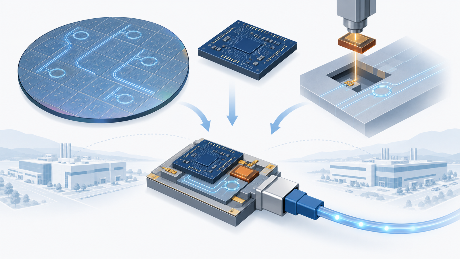
The biggest weakness of silicon photonics is that silicon cannot emit light. The lasers that supply the light have to be made separately in compound semiconductors such as InP and then connected to the photonic chip somehow. GF's technology page says on-chip lasers are in development, and in September 2026 it announced, with SMART Photonics, a foundry service that flip-chip mounts InP lasers and optical amplifiers into cavities etched into GF's silicon Sourced. The two companies say that "for more than a year" they carried out co-engineering and development to meet the technical requirements of dimensional fit and efficient optical coupling. GF's senior fellow said: "Our customers seek active components seamlessly integrated into our silicon photonics platform." From this we read that GF is aiming to go a step beyond contract manufacturing of photonic chips, towards handing customers a complete optical engine, light source included Not yet confirmed. For how light sources are integrated, see our explainers on semiconductor lasers and on photonic integrated circuits and indium phosphide.
9. Partnership map
10. Technologies, products and services
| Item | What the official materials say | Volume production or demonstration |
|---|---|---|
| First-generation process | Up to 100G per wavelength. 55 GHz bandwidth, 100 to 400 GHz channel spacing | In volume production (the company says it is widely adopted) |
| Second-generation process | Up to 200G per wavelength. Bandwidth above 65 GHz, 200 GHz channel spacing | Described as "proven" |
| Third-generation process | A path to 400G per wavelength | Early access (in development) |
| SCALE (for CPO) | Uses CWDM and DWDM to transmit and receive bidirectionally on a single fibre. Bidirectional DWDM with 8 and 16 wavelengths demonstrated. Detachable fibre allows scaling from 4 wavelengths per direction to 8 or more. The EIC is integrated in an advanced single-digit-nanometre process | Wavelength multiplexing at the demonstration stage. Targets of 400 Gb/s and 5x power efficiency |
| Qualified optical devices | 50 Gbps and 100 Gbps micro-ring modulators, coupled ring resonators and integrated photodiodes | Described as "fully-qualified" |
| Wavelength filters | Athermal CWDM filters: insertion loss below 1 dB, ripple below 0.2 dB, crosstalk below -30 dB | Described as "proven" |
| Packaging | TSVs; copper pad pitch from 110 µm to below 45 µm (2.5D/3D stacking from organic substrates to silicon interposers); detachable fibre connections | Available |
| SiGe (electrical side) | For the high-speed analogue circuits in optical transceivers. Current technology supports 200G per lane | In volume production (capacity being expanded for Marvell) |
| Light source integration | A foundry service that flip-chip mounts SMART Photonics' InP lasers and SOAs into cavities in GF's silicon. On-chip lasers are separately in development | General availability planned for the second half of 2027 |
"The industry's first OCI MSA capable platform" and "exceeds the requirements set by the OCI MSA" are GF's own claims Sourced. We could not find any material from the OCI MSA (Optical Compute Interconnect Multi-Source Agreement) itself recognising GF's product as compliant Not yet confirmed. How wavelength multiplexing and micro-rings work is covered in our explainers on wavelength multiplexing and micro-rings and on silicon photonics.
The foundry service with SMART Photonics places InP lasers upside down into cavities etched into a silicon wafer and bonds them there Sourced. The laser's output facet and the silicon waveguide are both light paths no more than a few micrometres wide, so unless their vertical and lateral positions line up to within a micrometre, almost no light gets in. The dimensions have to be dialled in right down to the cavity depth, the thickness of the bonding material (solder) and shrinkage after bonding, which is presumably why the two companies say they spent more than a year co-developing for "dimensional fit and efficient optical coupling" Not yet confirmed. InP and silicon also have different coefficients of thermal expansion, so the laser's own heat and repeated temperature cycling put stress on the joint. The more the light source is brought inside the package rather than attached externally, the more the choice of bonding materials and thermal design decides product lifetime.
11. The risks this company carries
| Risk | Details | Category |
|---|---|---|
| The award is not final | The US$300 million is at the letter of intent (LOI) stage, not a final award agreement | Sourced |
| Optics may still be small | Communications infrastructure and data center, which includes optics, was US$745 million in 2025, or 11% of total revenue. Silicon photonics revenue on its own is not disclosed. AMF was less than 1% of consolidated revenue | Sourced |
| Sluggish company-wide growth | 2025 revenue grew only 0.6% year on year, and smart mobile devices, its largest market, fell 12.1%. The company is relying on optics for growth | Sourced |
| Integrating acquisitions | It is pursuing integration across countries and companies in a short time: AMF (Singapore), InfiniLink (Egypt-based) and the SMART Photonics collaboration | Inference |
| Pace of CPO adoption | SCALE is for CPO, but the company itself writes that pluggables are today's mainstay. If CPO adoption is slow, the return on SCALE investment will be slow too | Inference |
| A controlling shareholder | The 20-F states that Mubadala, the majority shareholder, will continue to have significant control over the company. A company-wide matter, not specific to optics | Sourced |
| Competition from other foundries | TSMC (COUPE), Tower Semiconductor and UMC, all covered in this series, have also officially put forward silicon photonics foundry services | Our calculation |
12. Glossary
- Silicon photonics
- Building light paths (waveguides), modulators and photodetectors onto a silicon wafer using semiconductor manufacturing processes.
- CPO / NPO / LPO
- CPO places the optical transmit and receive functions in the same package as the chip; NPO places them right next to it. LPO is a pluggable module that drops the signal-processing DSP.
- OCI MSA
- Optical Compute Interconnect Multi-Source Agreement: an industry common specification for linking AI computers with light.
- CWDM / DWDM
- Wavelength division multiplexing, sending several wavelengths of light down one fibre. CWDM uses coarse wavelength spacing; DWDM uses fine spacing.
- SiGe
- Silicon germanium, used for high-speed analogue circuits; in optical transceivers it drives the lasers and amplifies received signals.
- InP
- Indium phosphide, a compound semiconductor that can emit light and the main material for communications lasers.
- Flip chip
- A mounting method in which a chip is turned upside down and bonded directly to a substrate or another chip with solder or similar.
- LOI (letter of intent)
- A document in which the parties set out the broad terms and their intentions before a final agreement. It is less legally binding than the final agreement.
13. References
- GLOBALFOUNDRIES Inc. Form 20-F for the fiscal year ended December 31, 2025 (filed with the U.S. SEC on 27 February 2026). The six product families, revenue by end market, R&D expense, headcount, the consideration and completion dates for AMF and InfiniLink, sites, and control by Mubadala. https://www.sec.gov/Archives/edgar/data/1709048/000170904826000022/gfs-20251231.htm
- GLOBALFOUNDRIES Inc. Fourth-quarter and full-year 2025 earnings release (Form 6-K exhibit, 11 February 2026). Description of the AMF and InfiniLink acquisitions. https://www.sec.gov/Archives/edgar/data/1709048/000170904826000012/globalfoundries4q2025earni.htm
- GLOBALFOUNDRIES Inc. First-quarter 2026 earnings release (Form 6-K exhibit, 5 May 2026). The SCALE announcement and the OFC 2026 announcements with SENKO, Corning, EXFO and Siluxtek. https://www.sec.gov/Archives/edgar/data/1709048/000170904826000111/globalfoundries1q2026earni.htm
- GLOBALFOUNDRIES Inc. Second-quarter 2026 earnings release (Form 6-K exhibit, 5 August 2026). The CEO's remarks on optical networking, the CHIPS award letter of intent and the quantum award letter of intent. https://www.sec.gov/Archives/edgar/data/1709048/000170904826000218/globalfoundries2q2026earni.htm
- GlobalFoundries Press release, "GlobalFoundries Acquires Advanced Micro Foundry, Accelerating Silicon Photonics Global Leadership and Expanding AI Infrastructure Portfolio" (dated 17 November 2025, posted 18 November). AMF's 200 mm line, the plan to move to 300 mm and the research centre with A*STAR. https://gf.com/news-and-events/news/globalfoundries-acquires-advanced-micro-foundry-accelerating-silicon-photonics-global-leadership-and-expanding-ai-infrastructure-portfolio/
- GlobalFoundries Press release, "GlobalFoundries accelerates adoption of co-packaged optics for advanced AI data centers with SCALE optical module solution" (4 May 2026). The make-up of SCALE and its optical devices. https://gf.com/news-and-events/news/globalfoundries-accelerates-adoption-of-co-packaged-optics-for-advanced-ai-data-centers-with-scale-optical-module-solution/
- GlobalFoundries Press release, "GlobalFoundries signs letter of intent with the U.S. Department of Commerce for a $300 million award to accelerate U.S. silicon photonics leadership" (29 July 2026). Award targets, SCALE targets, the Department of Commerce's shareholding and supporting comments from ten companies. https://investors.gf.com/news-releases/news-release-details/globalfoundries-signs-letter-intent-us-department-commerce-300
- GlobalFoundries Press release, "GlobalFoundries and Marvell expand collaboration for next-generation optical connectivity" (17 September 2026). SiGe capacity expansion, 200G-per-lane support and comments from the senior vice president for the Photonics & RF businesses. https://gf.com/news-and-events/news/globalfoundries-and-marvell-expand-collaboration-fornext-generation-optical-connectivity/
- SMART Photonics Press release, "SMART Photonics Partners with GlobalFoundries to Offer Industry’s First Open Access Foundry Service for Integrated Silicon and Indium Phosphide Photonics Products" (21 September 2026). Flip-chip integration of InP lasers and SOAs, more than a year of co-development and general availability in the second half of 2027. https://www.smartphotonics.nl/knowledge-hub/smart-photonics-partners-with-globalfoundries
- GlobalFoundries Technology page, "Silicon photonics". Supported form factors, first- to third-generation specifications, CWDM filters, manufacturing sites, on-chip lasers (in development) and collaboration with SENKO and Corning. https://gf.com/technologies/silicon-photonics/
- GlobalFoundries Official website (source of the company name style and the logo). https://gf.com/
14. Claim-to-source audit
| Claim in the article | Category | Source |
|---|---|---|
| Legal name, Cayman Islands exempted company, Mubadala as majority shareholder, headquarters address | Sourced | Reference 1 https://www.sec.gov/Archives/edgar/data/1709048/000170904826000022/gfs-20251231.htm |
| Revenue (2023 to 2025), communications infrastructure and data center revenue and share, its 29.1% growth in 2025 and the reasons | Sourced | Reference 1 https://www.sec.gov/Archives/edgar/data/1709048/000170904826000022/gfs-20251231.htm |
| R&D expense (2024 and 2025), about 14,000 employees and about 1,600 R&D staff | Sourced | Reference 1 https://www.sec.gov/Archives/edgar/data/1709048/000170904826000022/gfs-20251231.htm |
| Silicon photonics as one of six differentiated product families | Sourced | Reference 1 https://www.sec.gov/Archives/edgar/data/1709048/000170904826000022/gfs-20251231.htm |
| AMF consideration of US$453 million (cash), the two completion dates given, less than 1% of consolidated revenue and about 1% of total assets | Sourced | Reference 1 https://www.sec.gov/Archives/edgar/data/1709048/000170904826000022/gfs-20251231.htm |
| Acquisition of InfiniLink (14 November 2025, US$48 million) and its business | Sourced | References 1 and 2 https://www.sec.gov/Archives/edgar/data/1709048/000170904826000012/globalfoundries4q2025earni.htm |
| AMF's 200 mm line, the 300 mm plan, the research centre with A*STAR, the claim of being the largest pure-play foundry by revenue, sourcing from multiple regions | Sourced | Reference 5 https://gf.com/news-and-events/news/globalfoundries-acquires-advanced-micro-foundry-accelerating-silicon-photonics-global-leadership-and-expanding-ai-infrastructure-portfolio/ |
| OFC 2026 announcements with SENKO, Corning, EXFO and Siluxtek | Sourced | Reference 3 https://www.sec.gov/Archives/edgar/data/1709048/000170904826000111/globalfoundries1q2026earni.htm |
| SCALE's make-up (CWDM and DWDM, bidirectional DWDM with 8 and 16 wavelengths, qualified optical devices, TSVs, pad pitch, detachable fibre, the claim of OCI MSA capability) | Sourced | Reference 6 https://gf.com/news-and-events/news/globalfoundries-accelerates-adoption-of-co-packaged-optics-for-advanced-ai-data-centers-with-scale-optical-module-solution/ |
| The US$300 million CHIPS award letter of intent, its targets, SCALE targets (400 Gb/s, 5x power efficiency), the Department of Commerce's roughly 1% stake, the ten supporting comments, and the statement that GF supports today's pluggables | Sourced | Reference 7 https://investors.gf.com/news-releases/news-release-details/globalfoundries-signs-letter-intent-us-department-commerce-300 |
| The CEO naming optical networking as a strategic growth driver; the US$375 million quantum award letter of intent | Sourced | Reference 4 https://www.sec.gov/Archives/edgar/data/1709048/000170904826000218/globalfoundries2q2026earni.htm |
| The expanded SiGe agreement with Marvell, 200G-per-lane support, more than a decade of collaboration and SiGe manufacturing, the senior vice president for Photonics & RF | Sourced | Reference 8 https://gf.com/news-and-events/news/globalfoundries-and-marvell-expand-collaboration-fornext-generation-optical-connectivity/ |
| The InP laser integration service with SMART Photonics, more than a year of co-development, general availability in the second half of 2027, the senior fellow's comment | Sourced | Reference 9 https://www.smartphotonics.nl/knowledge-hub/smart-photonics-partners-with-globalfoundries |
| First- to third-generation process specifications, CWDM filter values, manufacturing sites, on-chip lasers (in development), the plan to onshore packaging, supported form factors | Sourced | Reference 10 https://gf.com/technologies/silicon-photonics/ |
| The three types of optical communications company | Our calculation | Our own classification. Example companies drawn from those covered in this series |
| Silicon photonics revenue and growth targets, optics-related capital spending and capacity, SCALE customers and volume timing, the names of the novel optical materials, the timing of the move to 300 mm | Not yet confirmed | Not stated in references 1 to 10. Press and research-firm figures are not used https://www.sec.gov/Archives/edgar/data/1709048/000170904826000022/gfs-20251231.htm |
| Timing and terms of a final CHIPS award agreement | Not yet confirmed | Still at the letter of intent stage, so not final https://investors.gf.com/news-releases/news-release-details/globalfoundries-signs-letter-intent-us-department-commerce-300 |
| Whether the OCI MSA itself recognises GF's product as compliant | Not yet confirmed | This article has confirmed only GF's own claim; no material from the standards body was found https://gf.com/news-and-events/news/globalfoundries-accelerates-adoption-of-co-packaged-optics-for-advanced-ai-data-centers-with-scale-optical-module-solution/ |
| How the share issuance to the Department of Commerce on 3 September 2026 relates to the optics award | Not yet confirmed | The 6-K does not state the link, so this article does not connect them (our own judgement) |
| The aims of assembling the parts for sending and receiving light within its own fabs, of winning customers who want diversified sourcing through two bases, and of making products not tied to any one customer through a common specification | Inference | This article's interpretation of references 5 to 10 taken together |
| The reading that pluggables, not CPO, are the main earner for now | Inference | This article's interpretation of the wording of references 7 and 9 |
| The reading that it aims to hand over complete optical engines, light source included | Inference | This article's interpretation of references 9 and 10 |
| The reading that replacing materials is the next-generation focus; the alignment and thermal challenges of InP laser integration | Inference | This article's commentary based on references 5, 7 and 9 and on the general properties of such devices |
| The risks of integrating acquisitions and of the pace of CPO adoption | Inference | This article's interpretation of references 1 and 7 |
| Other foundries also putting forward silicon photonics foundry services | Our calculation | Our own summary, based on the profiles of each company in this series |
Last updated 26 September 2026 / Troy Technical
Every figure in this article comes from filings GLOBALFOUNDRIES Inc. has made with the U.S. Securities and Exchange Commission (SEC), the company's official announcements and technology page, and its partners' official announcements. No research-firm estimates or press-based figures have been used. Passages marked "Inference" are this article's interpretation of the primary sources, not statements made by the company.