COMPANY PROFILE / OPTICAL COMMUNICATIONS & PHOTONICS
Mitsubishi Electric
100 million EML chips for data centres: a diversified electronics group redirecting power semiconductor investment into optical devices
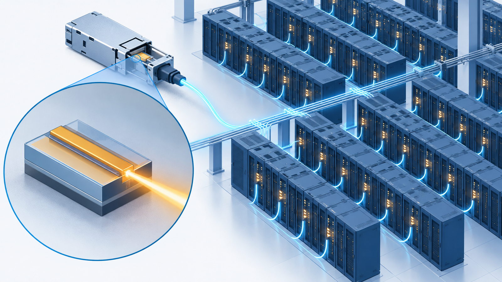
Mitsubishi Electric is a diversified electrical and electronics group with sales of ¥5.9 trillion, and optical communications is only a very small part of it. It still comes up in this field because it mass-produces EML chips, the transmit light sources inside the optical transceivers used in data centres, and has said publicly that it had shipped 100 million of them cumulatively by FY2025. In FY2025 it decided on a ¥40 billion investment to expand production, and it plans to raise EML chip production capacity to more than three times the FY2025 level by FY2029. This profile keeps the air-conditioning, factory automation, defence and other businesses to a minimum and concentrates on what the company is putting into optical devices, who it works with and where it is heading.
- Mitsubishi Electric in 30 seconds, and where it stands in optical communications and photonics
- The logo and how the name is written
- Where the company sits in the optical communications landscape
- Scale (the group in brief)
- Resources committed to optical communications and photonics
- What it has done so far
- What comes next
- What the company is aiming for in optical communications and photonics
- Map of relationships in optical communications and photonics
- Technologies, products and services
- The risks this company carries
- Glossary, references and claim-to-source audit
1. Mitsubishi Electric in 30 seconds, and where it stands in optical communications and photonics
(optical device chips)Supplies laser chips for optical transceivers
Light sources for optical transceiversAlso light sources for coherent and space optical communications
Companies involved in optical communications fall into three broad types: optical components & modules, chips & foundries, and network systems & carriers. Mitsubishi Electric's optical communications business is on the optical components side, and within that it makes only the "chips" that go inside optical transceivers Sourced. It does not make optical fibre, cable or the optical transceivers themselves. The May 2026 business presentation positions the company as a supplier of "EML chips for data centres" and says it has a multi-layered, solid customer base including hyperscalers and network system suppliers. In other words, Mitsubishi Electric takes part in optical communications as a compound semiconductor maker selling light-source chips to optical transceiver makers and, beyond them, to cloud operators.
2. The logo and how the name is written

The Mitsubishi Electric logo is a trademark of the company. We have not recreated it with generated imagery;
the image was taken from the official website and is placed here as img/mitsubishi_electric_logo.svg.
A note on names: the legal entity is Mitsubishi Electric Corporation. Optical devices belong to the High Frequency & Optical Device business within the "Semiconductor & Device business", and the segment name in the Annual Securities Report is "Semiconductor & Device". Among its manufacturing sites, the Kita-Itami Works, built in 1959 as a plant dedicated to volume production of semiconductors, is now the High Frequency & Optical Device Works and other facilities.
Official site: https://www.mitsubishielectric.co.jp/ja/3. Where the company sits in the optical communications landscape
In terms of where in the optical chain it operates, its core is inside the data centre: the transmit light sources (EML chips) and receive chips (pin-PDs) of the optical transceivers that carry traffic between servers. It is also developing light sources for long-haul digital coherent communications (a DFB-CAN with a built-in wavelength monitor) and laser source modules for space optical communications Sourced. The relationship between EMLs and CPO is easier to follow alongside our explainers on semiconductor lasers and co-packaged optics.
4. Scale (the group in brief)
The size of the group as a whole is covered in a single table Sourced.
| Measure | FY2024 (year to March 2025) | FY2025 (year to March 2026) |
|---|---|---|
| Consolidated net sales | ¥5,521.7 billion | ¥5,894.7 billion |
| Consolidated operating profit | ¥391.8 billion | ¥433.0 billion |
| Consolidated R&D expenses | - | ¥235.9 billion |
| Consolidated employees (people, 31 March 2026) | - | 150,386 |
FY2024 net sales and operating profit were back-calculated by us from the FY2025 values and the year-on-year increases given in the Annual Securities Report Our calculation
In the Annual Securities Report, optical devices are part of the "Semiconductor & Device" segment and are combined with power semiconductors. For optical figures alone we use those the company gave in its May 2026 business presentation and the accompanying Q&A summary Sourced.
| Figures relating to optical devices | FY2024 | FY2025 | FY2026 outlook | FY2030 target |
|---|---|---|---|---|
| Semiconductor & Device sales | ¥286.3 billion | ¥287.1 billion | ¥300 billion | ¥0.4 trillion |
| Same segment, adjusted operating margin | 14.2% (operating margin) | 16.1% | 14.3% | 20% |
| High Frequency & Optical Device sales | - | ¥55.4 billion | ¥73.0 billion | ¥100 billion |
| Data-centre EML chip sales | - | ¥40 billion | - | ¥80 billion |
Semiconductor & Device sales are only 4.9% of consolidated net sales, and the High Frequency & Optical Device business within it only 19.3% of that Our calculation. But since data-centre EML chips account for ¥40 billion of the business's ¥55.4 billion in sales, about 70% of this business is EMLs Our calculation. On the operating margin of optical devices, the company says it exceeds the whole division's FY2025 result (an adjusted operating margin of 16.1%) and is higher than that of power devices, but it has not published a specific figure Not yet confirmed. In the Q&A the company gave its FY2030 sales target for optical devices as "¥80 billion".
5. Resources committed to optical communications and photonics
| Type of resource | What it is | Category |
|---|---|---|
| People (dedicated organisation and staff) | The Semiconductor & Device segment has 5,556 employees (31 March 2026, of whom 2,114 at the parent company). The figure includes power semiconductors; headcount for optical devices alone is not disclosed. Manufacturing sites include the High Frequency & Optical Device Works | Sourced |
| Money (R&D) | R&D expenses in the Semiconductor & Device field of ¥19.2 billion (8.1% of consolidated R&D; the percentage is our calculation). Packaging technology for photonic-electronic convergence is developed under "Others and common" | Sourced |
| Money (capital expenditure) | Decided in FY2025 to invest ¥40 billion, raising EML chip production capacity by FY2029 to more than three times the FY2025 level (20 times the FY2020 level) | Sourced |
| Resource allocation policy | In May 2025 the company said it would restrain and defer investment in the power device business while shifting part of it to the strongly performing optical device business. In May 2026 it said that, with its up-front investment in power devices reaching a certain milestone, it would accelerate growth investment in the optical device business | Sourced |
| Outside investments, acquisitions and joint ventures | No investments or acquisitions in optical communications appear in the primary sources we checked (the investments listed in the May 2025 materials relate to SiC and gallium oxide power semiconductors) | Not confirmed |
| Public funding (NEDO, NICT and others) | No selection for subsidies or commissioned projects in optical communications appears in the primary sources we checked | Not confirmed |
| Links with universities and research institutes | The light source module for space optical communications was demonstrated aboard OPTIMAL-1, a microsatellite described as developed in an industry-academia collaboration project. No joint research with universities on EMLs for optical communications is mentioned | Partly sourced |
6. What it has done so far
| When | What happened | Why it matters |
|---|---|---|
| January 1921 | Founded by taking over the electrical machinery works of Mitsubishi Shipbuilding's Kobe Shipyard | The starting point as an electrical and electronics group |
| August 1959 | Builds the Kita-Itami Works (now the High Frequency & Optical Device Works and other facilities) as a plant dedicated to volume production of semiconductors | The origin of its optical device manufacturing base |
| March 2023 | Develops a 200 Gbps (112 Gbaud PAM4) EML chip for the four CWDM4 wavelengths. Its own hybrid waveguide structure doubles the operating speed of earlier chips | For 800G and 1.6T optical transceivers |
| March 2024 | Announces sample shipments of a DFB-CAN with a built-in wavelength monitor for digital coherent communications (in a TO-56 CAN, 1 W power consumption) | A light source for long-haul communications |
| April 2024 | Volume production begins of the 200 Gbps EML chip | Volume production of transmit light sources for the 1.6T generation |
| September 2024 | Achieves all success criteria in the in-orbit demonstration of a laser source module for space optical communications built from commercial components (no performance degradation over six months) | Described by the company as the world's first real-environment evaluation of optical component degradation in space |
| October 2024 | Begins sample shipments of a 200 Gbps pin-PD chip, its first receive-side optical device | Now covers both transmit and receive |
| May 2025 | Announces a policy of restraining and deferring power semiconductor investment and shifting part of it to the optical device business | Internal resource allocation moves towards optics |
| FY2025 | Data-centre EML chip sales of ¥40 billion and 100 million units shipped cumulatively. Decides on a ¥40 billion investment to expand production | The year EMLs became a pillar of the business |
| FY2025 | Develops flip-chip packaging technology without wire bonding, for photonic-electronic co-packaging (Annual Securities Report) | Packaging technology for CPO |
| October 2025 | With NTT East and the CC-Link Partner Association, succeeds in demonstrating real-time monitoring and control of industrial equipment up to 1,600 km away over the IOWN APN | A demonstration from the user side of an optical network |
| May 2026 | The new medium-term business strategy sets out EML chip capacity of more than three times by FY2029 and the market launch of CW light sources and modulator devices for CPO | A plan that looks beyond EMLs |
7. What comes next
According to the May 2026 business presentation and the Q&A summary, Mitsubishi Electric has set out the following policy for optical devices Sourced. (1) Following the 200 Gbps part for 1.6 Tbps, it will develop 300 Gbps and 400 Gbps EML chips in advance. (2) It will extend EMLs to short reaches of around 100 m, where low-cost VCSELs have been the norm (the company says replacement is under way as speeds rise to 800 Gbps and above). (3) For CPO, it will bring to market CW light sources and modulator devices using InP semiconductor technology. The company expects the CPO market to take off "around FY2028 to FY2029, with full-scale expansion in the 2030s", and says that EMLs (between servers) and CPO (within racks) will both grow while occupying separate areas of use. The FY2030 targets assume ¥140 to the US dollar.
None of the following appears in the primary sources Not yet confirmed.
Where the ¥40 billion production investment will be installed and the details of when it will start operating; the names of EML chip customers (the materials say only "hyperscalers and network system suppliers"); the amount of operating profit of the optical device business; and when the CW light sources and modulators for CPO will be launched. The company writes that it is "No. 1 in global share of EML chips for data centres", but the basis is given as "FY2024 results, company research" and no figures for the overall market are shown, so this article treats it as reference information only. The optical transceiver market size cited in the business presentation is a forecast by LightCounting, a research firm, and this article does not use it.
8. What the company is aiming for in optical communications and photonics
This section goes beyond what the company says directly. It sets out inferences that can be drawn from primary sources, each with its basis.
| What can be read | Primary evidence behind it | Category |
|---|---|---|
| It will not move into optical transceivers themselves but stick to being a chip supplier | The measures in the business presentation are limited to chip-level items such as EML chips, pin-PD chips, CW light sources and modulator devices; no plan to commercialise optical transceivers is mentioned | Inference |
| It is moving the main lever for improving margins in the semiconductor and device business from power semiconductors to optical devices | It cites "scaling up high-margin optical devices" as a reason it will reach a 20% adjusted operating margin, and is shifting power device investment to optics | Sourced |
| In CPO it will compete against thin-film LN with InP modulators | In the Q&A it said that TFLN has the drawback of large size, and that the company's strength is InP semiconductor modulators, which can be made small | Sourced |
| Until CPO takes off in earnest, it will earn from growing EML volumes | It expects the CPO market to take off in FY2028 to FY2029, while planning to raise EML capacity to more than three times by FY2029 | Inference |
| It has set its sales target deliberately conservatively | Against capacity of more than three times, the optical device sales target is ¥80 billion. The company gives as reasons the market-volatility risk peculiar to the IT industry and the lower unit price of short-reach EMLs, and says it wants to "firmly aim for ¥80 billion or more" | Sourced |
In the Q&A summary, the company describes its current EML chip as "a configuration in which an InP modulator is integrated with a CW (continuous wave) laser", and says that in next-generation CPO "these may be used separately" Sourced. In other words, in the CPO era the light source and the modulator, once combined on one chip, may be separated and bought from different companies. Mitsubishi Electric says that even in a form where the laser and modulator are separated, it can provide both as a single high-performance solution. Our reading is that the company is making its ability to sell separately the design and manufacturing skills for both light source and modulator, built up through EMLs, its survival strategy for the CPO era Not yet confirmed.
9. Map of relationships in optical communications and photonics
10. Technologies, products and services
| Product | What the primary sources say | Stage |
|---|---|---|
| 200 Gbps (112 Gbaud PAM4) EML chip | Covers the four CWDM4 wavelengths. Four chips make an 800 Gbps optical transceiver and eight a 1.6 Tbps one. A hybrid waveguide structure integrating a buried-type laser and a high-mesa modulator on the same chip | In volume production (since April 2024) |
| 200 Gbps pin-PD chip | For reception. A back-illuminated structure and an integrated convex lens shrink the photoelectric conversion area; compatible with flip-chip mounting | Samples (since October 2024) |
| DFB-CAN with built-in wavelength monitor | A light source for digital coherent communications. A wavelength monitor chip and a DFB laser chip housed in a TO-56 CAN; 1 W power consumption; wavelength 1547.72 nm | Samples (since April 2024) |
| Next-generation EML chips | 300 Gbps and 400 Gbps parts under advance development | In development |
| CW light sources and modulators for CPO | Light source and modulator devices using InP semiconductor technology. Flip-chip packaging technology for photonic-electronic co-packaging is also being developed | In development |
| Laser source module for space optical communications | Uses a 1.5 µm-band laser and is built from commercial components. No output degradation over six months in orbit | Demonstrated (commercialisation timing not disclosed) |
"Industry first" (use of a TO-56 CAN for a coherent light source) and "world first" (a real-environment evaluation of optical component degradation in space) are both the company's own wording. CWDM4 (four-wavelength multiplexing) is a scheme defined in an MSA, but Mitsubishi Electric's release does not state compliance with it, so this article says only that the chip "covers the four CWDM4 wavelengths".
Mitsubishi Electric's 200 Gbps EML chip is described as a "hybrid waveguide structure" that integrates on one chip a buried-type laser, which excels at high optical output, and a high-mesa modulator, which excels at high extinction ratio and wide bandwidth Sourced. In general, a buried structure fills in (regrows) both sides of the active layer with another semiconductor crystal, which lets heat escape and makes higher output easier, while a high-mesa structure carves the waveguide out deeply, giving low capacitance suited to high-speed modulation (our explanation). So this chip combines a step that "fills in" crystal and a step that "cuts deep" on a single InP wafer.
From the materials and process side, what matters here is the quality of the regrowth interface and the surface condition of the deeply etched sidewalls. Defects left in either feed straight into laser lifetime and modulator leakage current. Our reading is that the company's emphasis on "100 million units shipped" is a claim that it can run this difficult structure at volume-production yields Not yet confirmed. Yields and defect rates themselves have not been published.
11. The risks this company carries
| Risk | Substance | Category |
|---|---|---|
| IT market swings | The company itself cites market-volatility risk peculiar to the IT industry as a reason for setting its optical device sales target conservatively | Sourced |
| Falling unit prices | The company explains that short-reach EMLs tend to be priced lower than existing long-reach 200 Gbps parts, so more than tripling capacity does not translate into the same multiple of sales | Sourced |
| Changing configurations in CPO | The company itself acknowledges that in CPO the light source and modulator may be separated, and that thin-film LN (TFLN) may be used for the modulator | Sourced |
| Customers hard to see | Customer names are not disclosed, so concentration on particular customers cannot be checked from outside | Not yet confirmed |
| Small business scale | The High Frequency & Optical Device business is about 1% of consolidated sales. Its priority within the group depends on investment allocation policy | Inference |
| Exchange rates | The FY2030 targets assume ¥140 to the US dollar. A stronger yen would push down sales in yen terms | Sourced |
12. Glossary
- EML
- Electro-absorption Modulator integrated Laser diode. A semiconductor laser with an integrated electro-absorption optical modulator. The transmit light source in data-centre optical transceivers.
- pin-PD
- pin photodiode. A receiving element that converts optical signals into electrical signals.
- PAM4
- Four-level pulse amplitude modulation. Sends two bits per symbol.
- CWDM4
- A scheme that sends four wavelengths together over one fibre. Four wavelengths at 200 Gbps each make 800 Gbps.
- CW laser
- Continuous Wave. A laser that emits light of constant intensity continuously. Used, for example, as the external light source in CPO.
- VCSEL
- Vertical-cavity surface-emitting laser. Low-cost and used for short reaches, but the company says it faces challenges at very high speeds.
- TFLN
- Thin-Film Lithium Niobate. Attracting attention as a material for high-speed modulators.
- DFB-CAN
- A light source component in which a DFB laser chip is housed in a metal can-type package (TO-CAN).
13. References
- Mitsubishi Electric Corporation Annual Securities Report for the 155th fiscal period (1 April 2025 to 31 March 2026), filed 19 June 2026 (in Japanese). Company history, consolidated results, segment results, R&D activities (including packaging technology for photonic-electronic convergence) and headcount. https://www.mitsubishielectric.co.jp/investors/data/negotiable-securities/pdf/155.pdf
- Mitsubishi Electric Corporation IR Day 2026: Semiconductor & Device Business 2026 (29 May 2026, in Japanese). Financial targets, expansion of EML chip capacity (¥40 billion, more than three times), 100 million units shipped cumulatively, CW light sources and modulators for CPO, and the description of the customer base. https://www.mitsubishielectric.co.jp/ja/pr/2026/pdf/0529_co5.pdf
- Mitsubishi Electric Corporation Mitsubishi Electric IR Day 2026 business strategy: summary of questions and answers (8 June 2026, in Japanese). EML chip sales (¥40 billion to ¥80 billion), the ¥80 billion optical device sales target, the CPO market outlook, InP modulators and TFLN, and advance development of 300G and 400G EMLs. https://www.mitsubishielectric.co.jp/ja/pr/2026/pdf/0529_co7.pdf
- Mitsubishi Electric Corporation Semiconductor & Device business (28 May 2025, in Japanese). FY2024 results and the policy of shifting part of power device investment to optical devices. https://www.mitsubishielectric.co.jp/ja/pr/2025/pdf/0528-5.pdf
- Mitsubishi Electric Corporation News release: Development of a CWDM4-wavelength "200 Gbps (112 Gbaud PAM4) EML chip" (2 March 2023, in Japanese). https://www.mitsubishielectric.co.jp/ja/pr/2023/pdf/0302-b.pdf
- Mitsubishi Electric Corporation News release: Mitsubishi Electric to Ship Samples of 200Gbps PIN-PD Chip for Both 800Gbps and 1.6Tbps Optical-fiber Communication (20 August 2024; title of the English version, link to the Japanese release). Includes volume production of the 200 Gbps EML chip from April 2024. https://www.mitsubishielectric.co.jp/ja/pr/2024/0820/
- Mitsubishi Electric Corporation News release: Mitsubishi Electric to Ship Samples of DFB-CAN with Built-in Wavelength Monitor for Digital Coherent Information & Communication Systems (21 March 2024; title of the English version, link to the Japanese release). https://www.mitsubishielectric.co.jp/ja/pr/2024/0321/
- Mitsubishi Electric Corporation News release: Mitsubishi Electric Achieves All Success Criteria for Orbital Demonstration of the Laser Source Module for Space Optical Communication (19 September 2024; title of the English version, link to the Japanese release). https://www.mitsubishielectric.co.jp/ja/pr/2024/0919-a/
- NTT East, Mitsubishi Electric and the CC-Link Partner Association Press announcement: Successful demonstration of long-distance real-time communication over the industrial network CC-Link IE TSN using the IOWN APN (8 October 2025, in Japanese). https://www.mitsubishielectric.co.jp/ja/pr/2025/pdf/1008-b.pdf
- Mitsubishi Electric Corporation Official website (source of the company name and logo image). https://www.mitsubishielectric.co.jp/ja/
14. Claim-to-source audit
| Claim in the article | Category | Source |
|---|---|---|
| Legal name, head office address, founding in 1921, the Kita-Itami Works of 1959 (now the High Frequency & Optical Device Works and other facilities) | Sourced | Reference 1 https://www.mitsubishielectric.co.jp/investors/data/negotiable-securities/pdf/155.pdf |
| Consolidated net sales, operating profit, R&D expenses and headcount; Semiconductor & Device sales, R&D expenses and headcount | Sourced | Reference 1 https://www.mitsubishielectric.co.jp/investors/data/negotiable-securities/pdf/155.pdf |
| Development of flip-chip packaging technology for photonic-electronic co-packaging | Sourced | Reference 1 https://www.mitsubishielectric.co.jp/investors/data/negotiable-securities/pdf/155.pdf |
| FY2025 results, FY2026 outlook and FY2030 targets for the semiconductor and device business; High Frequency & Optical Device sales (¥55.4 billion, ¥73.0 billion, ¥100 billion); assumed exchange rate | Sourced | Reference 2 https://www.mitsubishielectric.co.jp/ja/pr/2026/pdf/0529_co5.pdf |
| The ¥40 billion investment, more than three times by FY2029 (20 times FY2020), 100 million units cumulatively, CW light sources and modulators for CPO, the description of the customer base, accelerated growth investment in optical devices | Sourced | Reference 2 https://www.mitsubishielectric.co.jp/ja/pr/2026/pdf/0529_co5.pdf |
| EML chip sales from ¥40 billion to ¥80 billion, the ¥80 billion optical device sales target and its reasons, the timing of the CPO take-off, InP modulators and TFLN, advance development of 300G and 400G parts, the explanation of optical device margins | Sourced | Reference 3 https://www.mitsubishielectric.co.jp/ja/pr/2026/pdf/0529_co7.pdf |
| FY2024 semiconductor and device sales of ¥286.3 billion and operating margin of 14.2%, shifting part of power device investment to optical devices | Sourced | Reference 4 https://www.mitsubishielectric.co.jp/ja/pr/2025/pdf/0528-5.pdf |
| Development of the 200 Gbps EML chip and its hybrid waveguide structure | Sourced | Reference 5 https://www.mitsubishielectric.co.jp/ja/pr/2023/pdf/0302-b.pdf |
| Sample shipments of the 200 Gbps pin-PD chip, and volume production of the 200 Gbps EML chip from April 2024 | Sourced | Reference 6 https://www.mitsubishielectric.co.jp/ja/pr/2024/0820/ |
| Specifications and sample shipments of the DFB-CAN with built-in wavelength monitor | Sourced | Reference 7 https://www.mitsubishielectric.co.jp/ja/pr/2024/0321/ |
| The in-orbit demonstration of the light source module for space optical communications, and OPTIMAL-1 | Sourced | Reference 8 https://www.mitsubishielectric.co.jp/ja/pr/2024/0919-a/ |
| The demonstration of real-time monitoring and control over up to 1,600 km using the IOWN APN | Sourced | Reference 9 https://www.mitsubishielectric.co.jp/ja/pr/2025/pdf/1008-b.pdf |
| 4.9% of consolidated sales, 19.3% for High Frequency & Optical Devices, EMLs at about 70%, 8.1% of R&D, back-calculated FY2024 values | Our calculation | Calculated by this article from figures in references 1 to 3 |
| The three types of optical communications company | Our calculation | Our own classification. Companies shown are examples from those in this series |
| The amount of optical device operating profit, the location and start-up timing of the production investment, customer names, the launch timing of products for CPO | Not yet confirmed | Not in references 2 and 3. Figures from press reports are not used https://www.mitsubishielectric.co.jp/ja/pr/2026/pdf/0529_co5.pdf |
| "No. 1 in global share" (company research), and the research-firm market forecast in the business presentation | Not yet confirmed | Not used as figures because they are the company's own research or a research-firm estimate https://www.mitsubishielectric.co.jp/ja/pr/2026/pdf/0529_co5.pdf |
| Investments or acquisitions in optical communications, public funding awarded, joint research with universities | Not yet confirmed | Not in the primary sources we checked. This article does not conclude that none exists https://www.mitsubishielectric.co.jp/investors/data/negotiable-securities/pdf/155.pdf |
| The reading that it will stick to being a chip supplier, and that it will earn from EML volumes until CPO takes off in earnest | Inference | This article's interpretation of references 2 and 3 |
| The reading that selling light source and modulator separately is its survival strategy for the CPO era | Inference | This article's interpretation of the Q&A in reference 3 |
| The explanation of the structural difference between buried and high-mesa types, and the reading that 100 million units is a claim about volume-production yields | Not yet confirmed | This article's explanation, based on general knowledge of optical semiconductors |
| The risk of small business scale | Inference | This article's interpretation of references 1 and 2 |
Last updated 26 September 2026 / Troy Technical
Every figure in this article comes from the Annual Securities Report, business presentations, Q&A summary and news releases published by Mitsubishi Electric Corporation. No research-firm estimates or press-based figures have been used. Passages marked "Inference" are this article's interpretation of primary sources, not statements made by the company.