COMPANY PROFILE / OPTICAL COMMUNICATIONS & PHOTONICS
Nokia
The European network equipment maker that bought Infinera, and with it an optical chip fab
Nokia was long known for mobile phones, but today it makes the equipment that telecoms networks run on. In optical communications, it acquired Infinera of the United States for €2.5 billion in February 2025, lifting revenue in its Optical Networks business about 1.8-fold in a year, to €3,019 million. In April to June 2026, Optical Networks grew another 20% year on year at constant currency, with orders from AI and cloud customers rising. What sets it apart is that it does not just make optical transport systems: it makes the indium phosphide (InP) optical chips inside them in its own fabs, and it keeps adding manufacturing capacity in the United States. This profile sets out the optics business using only the annual and quarterly reports Nokia has filed with the U.S. SEC and its official releases.
- Nokia in 30 seconds, and where it stands in optical communications and photonics
- The logo and how the name is written
- Where the company sits in optical communications and photonics
- Scale (the company in brief, the optics business in numbers)
- Resources committed to optical communications and photonics
- What it has done so far
- What comes next
- What the company is aiming for in optical communications and photonics
- Map of partnerships in optical communications and photonics
- Technologies, products and services
- The risks this company carries
- Glossary, references and claim-to-source audit
1. Nokia in 30 seconds, and where it stands in optical communications and photonics
FinlandKarakaari 7
NYSE (ADS)Tickers NOKIA / NOK
(makes its own optical chips)Owns an InP optical chip fab in the United States
links between data centresMetro, regional, long-haul and DCI
under the CHIPS ActDirect funding from the U.S. Department of Commerce (per the 20-F)
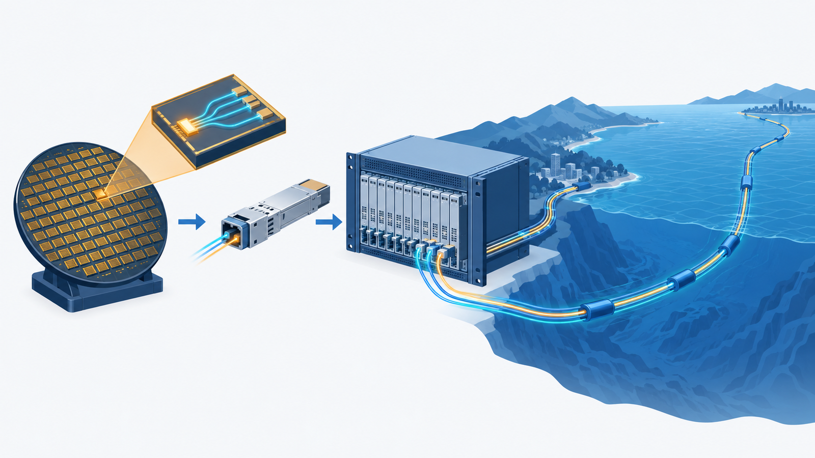
This series sorts companies in optical communications and photonics into three types: optical components & modules, chips & foundries, and network systems & carriers. Nokia is a network systems maker, but it does not simply buy its optical parts in. According to its 20-F, the Infinera acquisition "gave Nokia the capability to build key optical semiconductor components with its internal Indium Phosphide (InP) wafer fab capability in California", and the company itself says that "having capability in-house derisks a critical element of our supply chain" Sourced. In other words, Nokia holds the whole vertical chain within one company: optical transport systems, the coherent optical modules inside them, and the InP optical chips inside those.
2. The logo and how the name is written

The Nokia logo is a trademark of the company. We have not recreated it with generated imagery;
the logo image (SVG) used in the header of the official website (nokia.com) is placed here as img/nokia_logo.svg.
A note on names: the English legal name is Nokia Corporation; in Finnish it is Nokia Oyj. The Nokia in this article is Nokia the maker of network equipment. Infinera (formerly Infinera Corporation of San Jose, U.S.), which it acquired, is now part of Nokia, and no separate results are disclosed for it.
Official site: https://www.nokia.com/newsroom/nokia-completes-acquisition-of-infinera-to-create-innovation-powerhouse-in-optical-networks-with-the-scale-to-power-the-data-center-revolution/3. Where the company sits in optical communications and photonics
In terms of where it works with light, Nokia's Optical Networks is the business that provides optical transport networks for metro, regional, long-haul and data centre interconnect (DCI) applications Sourced (per the segment description in the quarterly report). The 20-F also says that Optical Networks is "taking steps to address new emerging intra-data center component opportunities", so moving inside the data centre is on its horizon too. Fibre-to-the-home (PON) sits in a separate business unit, Fixed Networks, and is outside the scope of this article. The technologies covered in our explainers on coherent optical communication and DSPs and on photonic integrated circuits and indium phosphide are at the heart of its optics business.
| Aspect | Where Nokia stands | Category |
|---|---|---|
| Type | Network systems maker. Also makes optical semiconductors (InP photonic integrated circuits) in its own fabs | Sourced |
| Where it works with light (main) | Optical transport networks including metro, regional, long-haul and undersea; links between data centres | Sourced |
| Where it works with light (new) | Components inside the data centre, which the 20-F calls "new emerging" opportunities | Sourced |
| Customers | Telecoms operators, AI and cloud companies, and mission-critical and defence enterprises | Sourced |
| CPO (co-packaged optics) | No CPO product appears in the 20-F or quarterly report we checked | Not confirmed |
4. Scale (the company in brief, the optics business in numbers)
Nokia discloses revenue for its optics business (Optical Networks), so the company as a whole is kept brief and the focus is on the optics figures Sourced.
| Measure (€ million) | Year to December 2024 | Year to December 2025 | January to June 2026 |
|---|---|---|---|
| Nokia net sales | 19,220 | 19,889 | - |
| Group R&D expenses | 4,512 | 4,855 | - |
| Average employees | 78,434 | 78,005 | - |
| Network Infrastructure net sales | 6,518 | 7,986 | 3,866 |
| of which Optical Networks net sales | 1,636 | 3,019 | 1,689 |
| Network Infrastructure R&D expenses | 1,207 | 1,536 | - |
The January to June 2026 figures exclude two businesses reclassified as discontinued operations in April to June 2026 (Fixed Wireless Access CPE and Enterprise Campus Edge). Optical Networks in the same period a year earlier: €1,255 million.
Optical Networks' revenue rose by €1,383 million in 2025, and the 20-F says €1,273 million of that came from the Infinera acquisition Sourced. Taking that out leaves growth of about €110 million (about 6.7% year on year) from sources other than the acquisition Our calculation. The 20-F says currency movements had a negative effect of about 5%, so underlying growth at constant currency was larger than this. The rapid expansion of the optics business in 2025 was mainly the result of the acquisition; growth since the start of 2026 (+20% at constant currency in April to June) is the first measure of what the combined business can do.
In 2025, Optical Networks accounted for about 37.8% of Network Infrastructure revenue and about 15.2% of Nokia's total. In April to June 2026 its share of Network Infrastructure rose to about 42.6% Our calculation.
The 20-F describes Optical Networks as holding a "number two global market position", but the footnote supporting that claim cites estimates from research firms (Omdia and Dell'Oro). Because this article does not use research-firm estimates, no ranking or market share is given here. For the same reason, we do not use the "addressable market in 2028" figures in the 20-F, which are estimates that include analyst reports.
5. Resources committed to optical communications and photonics
| Type of resource | What it is | Category |
|---|---|---|
| People (dedicated organisation and staff) | Handled by the Optical Networks business unit within the Network Infrastructure segment. The Infinera team joined Optical Networks at the acquisition. David Heard, former CEO of Infinera, was leading Network Infrastructure at the time of the November 2025 strategy announcement. Headcount in the optics business is not disclosed | Sourced / headcount not disclosed |
| Money (R&D spending and capital expenditure) | Network Infrastructure R&D expenses were €1,536 million (2025, up 27% year on year, mainly because of the Infinera acquisition and higher investment). Group capital expenditure for 2026 is expected at €800 to 900 million, and the company states that it "continues to invest in expanding Optical manufacturing capacity". R&D and capital spending for the optics business alone are not disclosed | Sourced / optics-only figures not disclosed |
| Outside investments, acquisitions and joint ventures | Acquired Infinera for a consideration of €2.5 billion (completed 28 February 2025). In 2026 signed a definitive agreement to acquire NXP's semiconductor fab in Chandler, Arizona (full acquisition expected in Q1 2029) | Sourced |
| Universities, research institutes and public funding | US$93 million in direct funding from the U.S. Department of Commerce under the U.S. CHIPS Act. Of this, US$40 million goes to expanding the California fab, and up to US$53 million may also be used for a photonics packaging and testing project in Pennsylvania. The company says research at its in-house lab, Nokia Bell Labs, underpins its optical technology. No university research collaboration on optics has been confirmed | Sourced / universities not confirmed |
| Optical manufacturing site (U.S.) | Role | Size and timing |
|---|---|---|
| Sunnyvale, California (leased) | Compound semiconductor wafer fab and test facility | 2,300 m² (end of 2025) |
| San Jose, California | New compound semiconductor wafer fab. A previously leased facility was purchased in February 2026 | The 20-F says production is expected to begin in 2027; the July quarterly report says production will begin ramping later in Q4 2026. To reach 2,600 m² by 2028 |
| Allentown, Pennsylvania | Production and development of advanced packaging and test of photonic integrated circuits | 2,400 m² (owned), plus about 1,800 m² additionally leased in February 2026. Investment to increase capacity 10× from Q3 2026 |
| Chandler, Arizona (NXP's fab) | Planned conversion to InP semiconductor production | Part of the site to be leased from early 2027; full acquisition expected in Q1 2029 (subject to regulatory approvals) |
6. What it has done so far
| When | What happened | Why it matters |
|---|---|---|
| June 2024 | Announces the acquisition of Infinera | Aimed at scaling up the optics business and gaining a foothold in North America and with large cloud companies |
| 28 February 2025 | Completes the acquisition of Infinera (consideration €2.5 billion). The Infinera team joins Optical Networks | Gained an InP wafer fab and a packaging site |
| 2025 | Launches 800G ZR/ZR+ coherent pluggables. €2.4 billion in orders from AI and cloud customers over the year (group-wide) | Pluggable products for links between data centres |
| November 2025 | Announces a new strategy. Network Infrastructure is recognised as a "growth segment", with a target of 10 to 12% annual growth for optical and IP combined over 2025 to 2028 | Made optics a pillar of the company's growth |
| February 2026 | Buys the San Jose facility (for the new wafer fab). Leases an additional site in Allentown | Adds InP production capacity |
| April to June 2026 | Optical Networks revenue up 20% year on year (constant currency). AI and cloud orders of €2.8 billion in the quarter (optical and IP combined). Announces an investment to increase Allentown's capacity tenfold, and an agreement to acquire NXP's Chandler fab | The company says that against this demand, "supply continues to be the main industry constraint" |
| September 2026 | Nokia announces that Telxius will deploy Nokia's 800G coherent pluggables (ICE-X) in its terrestrial network. An earlier trial on the BRUSA subsea cable delivered 400 Gb/s per wavelength over more than 5,600 km | An adoption by a carrier |
7. What comes next
in 2026July 2026 outlook (optical and IP combined)
over 2025 to 2028Optical and IP combined. November 2025 strategy announcement
later in Q4 2026Expansion work continues to 2028
acquired in 2029To be converted to InP production. Subject to approvals
In its July quarterly report, the company says its U.S. manufacturing investments "support the demand expected in 2027 and 2028" Not yet confirmed. On AI and cloud orders in April to June, it writes that it expects "around half of these orders to convert to revenue over the next twelve months", and that "demand remains strong, while supply continues to be the main industry constraint", which suggests customers are placing long-term orders Sourced.
None of the following appears in the 20-F, quarterly report or releases Not yet confirmed.
Profit for Optical Networks (disclosure stops at Network Infrastructure as a whole); headcount in the optics business; the production capacity of the InP fabs (wafers or components); the names of AI and cloud customers; specific products and timing for components inside the data centre; and the price of NXP's Chandler fab.
8. What the company is aiming for in optical communications and photonics
This section goes beyond what the company says directly. It sets out inferences that can be drawn from primary sources, each with its basis.
| What can be read | Primary evidence behind it | Category |
|---|---|---|
| Optics has been placed at the centre of the company's growth | The November 2025 strategy made Network Infrastructure a "growth segment", and the 20-F states that investment in optical and IP will increase | Sourced |
| It wants owning its own optical semiconductors to be the source of its competitiveness | The 20-F says "we are also leaders in Indium Phosphide photonic integrated circuits, differentiating us from our competitors", and the company keeps buying, expanding and acquiring fabs | Inference |
| It wants to make U.S. supply capacity a selling point | The quarterly report says it is adding U.S.-based InP capacity "at a time when secure and scalable domestic supply is becoming increasingly important". It has also received CHIPS Act funding | Inference |
| In time it wants to sell optical components inside the data centre as well | The 20-F says it is taking steps to address "new emerging intra-data center component opportunities", and lists intra-data center optics among its R&D areas. No specific product has been announced | Inference |
| Through Infinera it wants to break into North America and the large cloud companies | The 20-F gives three aims for the acquisition: greater scale in optics, an expanded presence in North America, and a stronger position in AI and cloud | Sourced |
Every manufacturing plan Nokia has announced in 2026 is in the United States, and every one of them centres on a single material, InP: the new San Jose wafer fab, the tenfold increase in packaging and test capacity in Allentown, and the plan to convert NXP's Chandler fab to InP semiconductor production Sourced. InP is the compound semiconductor used to make the lasers, modulators and photodetectors for optical communications; it is the key to the light-emitting parts that are hard to make in silicon. In the quarterly report, the company says the Chandler acquisition "further strengthens Nokia's in-house compound semiconductor manufacturing capabilities through the addition of a highly experienced team". We read this as a judgement that the InP optical chip ultimately determines the performance and supply of optical transport systems, and that this is not something to depend on others for Not yet confirmed. When the company itself writes that demand is strong but "supply continues to be the main industry constraint", owning its own fabs can translate directly into the ability to win orders.
9. Map of partnerships in optical communications and photonics
10. Technologies, products and services
All figures are the company's own and are not third-party measurements. We found no material expressing power consumption per bit (pJ/bit).
| Product or technology | What it does | Main points the company gives | Stage |
|---|---|---|---|
| Coherent transponders (1.2T / 1.6T) | Units inside optical transport systems that put a large-capacity signal on a single wavelength | The 20-F cites "rapid adoption of high-speed optical transmission technology including 1.2T/1.6T coherent transponders" | Offered commercially (shipment volumes not disclosed) |
| ICE-X 800G ZR/ZR+ coherent pluggables | Pluggable modules that plug straight into routers for links between data centres and over long distances | In a trial on the BRUSA subsea cable, 400 Gb/s per wavelength over more than 5,600 km (the company calls it an "industry-record"). Deployed by Telxius in its terrestrial networks in Europe, the U.S. and Latin America | In volume production and being deployed (the trial figures are a demonstration) |
| InP photonic integrated circuits | Lasers, modulators, photodetectors and more integrated on a single InP chip | Made in its own wafer fab in California. The 20-F claims leadership in InP photonic integrated circuits, "differentiating us from our competitors" | Made in house |
| Packaging and test of photonic integrated circuits | The process of assembling InP chips into components and testing them | Allentown, Pennsylvania. Investment to increase capacity tenfold | Expansion from Q3 2026 |
| Components for inside the data centre | Components for optical connections inside the data centre | The 20-F says it is addressing these as "new emerging" opportunities | No product announced |
Indium phosphide (InP), where Nokia is adding capacity, is a compound semiconductor that can emit, modulate and detect light in the wavelength bands used for optical communications (1.3 μm and 1.55 μm) Not yet confirmed. Silicon cannot emit light, so even silicon photonics needs another material for its lasers. The strength of InP photonic integrated circuits is that everything from the laser to the photodetector can be integrated on one chip.
On the other hand, compared with silicon, InP comes in smaller wafer diameters, is brittle and easily cracked, and is an expensive material, so high-volume process flows cannot simply be borrowed. The quality of epitaxial growth (depositing thin crystal layers), the coating of facets, and the yield of packaging and testing when chips are assembled into components determine supply directly. One reading of why Nokia is strengthening its wafer fabs (San Jose, Sunnyvale, Chandler) and its packaging and test site (Allentown) separately is that either stage can become a supply constraint Not yet confirmed. For more, see our explainers on photonic integrated circuits and indium phosphide and on semiconductor lasers.
11. The risks this company carries
| Risk | Substance | Category |
|---|---|---|
| Supply capacity falling short | The company itself writes that "supply continues to be the main industry constraint". If fab ramps are delayed, orders cannot be turned into revenue | Sourced |
| Shifts in fab ramp timing | For the new San Jose fab, the 20-F (March 2026) says production begins in 2027, while the July quarterly report says the ramp begins later in Q4 2026; the wording differs. The NXP fab acquisition is in 2029 and subject to approvals | Sourced |
| Post-acquisition performance still unproven | Most of the optics revenue growth in 2025 came from the acquisition. Growth excluding it was about 6.7% (our calculation), so an assessment of underlying strength depends on figures from 2026 on | Our calculation |
| Intense competition | The risk factors in the quarterly report say competitive intensity "is expected to continue at a high level as some competitors seek to take share" | Sourced |
| Optics profitability not visible | Profit is disclosed only for Network Infrastructure as a whole, so the standalone economics of the optics business cannot be seen from outside | Sourced |
| Moving inside the data centre is an unknown | Components for inside the data centre are still at the "new emerging opportunity" stage, with no product or customer announced | Inference |
12. Glossary
- Indium phosphide (InP)
- A compound semiconductor that can emit and detect light at optical communication wavelengths. The material for lasers and photodetectors.
- Photonic integrated circuit (PIC)
- A chip that brings together optical components such as lasers, modulators and photodetectors.
- Coherent optical communication
- A method that carries information not only in the intensity of light but also in its phase and polarisation. Suited to long distances and high capacity.
- Transponder
- A unit inside an optical transport system that converts electrical signals into optical signals for long-distance transmission.
- ZR / ZR+
- Names for specifications of pluggable coherent optical modules that plug directly into routers. ZR+ supports longer distances.
- DCI
- Data Center Interconnect. Optical links between data centres.
- CHIPS Act
- U.S. legislation supporting domestic semiconductor production, under which the U.S. Department of Commerce provides grants and other funding.
- Form 20-F
- The annual report a foreign company listed in the United States files with the SEC. It is audited and carries legal liability for its contents.
13. References
- Nokia Corporation Annual Report on Form 20-F for the year ended 31 December 2025 (filed with the U.S. SEC on 5 March 2026). Optical Networks revenue and description, the Infinera acquisition (consideration, completion date, rationale), the InP wafer fab, manufacturing sites, CHIPS Act funding, R&D expenses, average headcount, strategy, and the market-position statement and its sources. https://www.sec.gov/Archives/edgar/data/924613/000162828026015034/nok-20251231.htm
- Nokia Corporation Report for Q2 and Half Year 2026 (Form 6-K, 23 July 2026). Optical Networks quarterly and half-year revenue, AI and cloud orders, the 2026 outlook, capital expenditure, the San Jose fab, Allentown and NXP's Chandler fab, risk factors, and the segment descriptions. https://www.sec.gov/Archives/edgar/data/924613/000110465926086081/tm2621179d1_6k.htm
- Nokia Corporation Stock exchange release, "Nokia announces new strategy, evolution of its operating model, new long-term financial target, strategic KPIs and changes to its Group Leadership Team" (Form 6-K, 19 November 2025). The positioning of Network Infrastructure, the 2025 to 2028 growth target for optical and IP, David Heard. https://www.sec.gov/Archives/edgar/data/924613/000110465925113946/tm2531737d1_6k.htm
- Nokia Corporation Press release, "Nokia completes acquisition of Infinera to create innovation powerhouse in optical networks, with the scale to power the data center revolution" (28 February 2025). https://www.nokia.com/newsroom/nokia-completes-acquisition-of-infinera-to-create-innovation-powerhouse-in-optical-networks-with-the-scale-to-power-the-data-center-revolution/
- Nokia Corporation Press release, "Telxius boosts global network capacity and efficiency with Nokia 800G coherent pluggable deployment" (15 September 2026). Deployment of ICE-X 800G ZR/ZR+ and the results of the trial on the BRUSA subsea cable. https://www.nokia.com/newsroom/telxius-boosts-global-network-capacity-and-efficiency-with-nokia-800g-coherent-pluggable-deployment/
14. Claim-to-source audit
| Claim in the article | Category | Source |
|---|---|---|
| Legal name, head office address, listing venues (Nasdaq Helsinki, NYSE) | Sourced | References 1 and 2 https://www.sec.gov/Archives/edgar/data/924613/000162828026015034/nok-20251231.htm |
| Group net sales, R&D expenses and average headcount (2024 and 2025) | Sourced | Reference 1 https://www.sec.gov/Archives/edgar/data/924613/000162828026015034/nok-20251231.htm |
| Network Infrastructure and Optical Networks net sales (2024 and 2025), Infinera's contribution of €1,273 million, Network Infrastructure R&D expenses | Sourced | Reference 1 https://www.sec.gov/Archives/edgar/data/924613/000162828026015034/nok-20251231.htm |
| Optical Networks revenue and growth in April to June and the first half of 2026, AI and cloud orders of €2.8 billion, "supply continues to be the main industry constraint" | Sourced | Reference 2 https://www.sec.gov/Archives/edgar/data/924613/000110465926086081/tm2621179d1_6k.htm |
| Growth excluding the acquisition of about €110 million (about 6.7%); Optical Networks' shares (about 37.8%, about 15.2% and about 42.6%) | Our calculation | Calculated in this article from the figures in references 1 and 2 https://www.sec.gov/Archives/edgar/data/924613/000162828026015034/nok-20251231.htm |
| Completion date, €2.5 billion consideration and three aims of the Infinera acquisition; reduced supply chain risk from the InP wafer fab | Sourced | References 1 and 4 https://www.sec.gov/Archives/edgar/data/924613/000162828026015034/nok-20251231.htm |
| The Infinera team joining Optical Networks; David Heard's role | Sourced | References 4 and 3 https://www.nokia.com/newsroom/nokia-completes-acquisition-of-infinera-to-create-innovation-powerhouse-in-optical-networks-with-the-scale-to-power-the-data-center-revolution/ |
| Size and timing of the manufacturing sites (Sunnyvale, Allentown, San Jose); US$93 million in CHIPS Act funding | Sourced | Reference 1 https://www.sec.gov/Archives/edgar/data/924613/000162828026015034/nok-20251231.htm |
| Timing of the San Jose fab ramp (later in Q4 2026), the tenfold Allentown increase, the agreement to acquire NXP's Chandler fab | Sourced | Reference 2 https://www.sec.gov/Archives/edgar/data/924613/000110465926086081/tm2621179d1_6k.htm |
| Expected optical and IP growth of 18 to 20% in 2026, capital expenditure of €800 to 900 million, continued investment in optical manufacturing capacity | Sourced | Reference 2 https://www.sec.gov/Archives/edgar/data/924613/000110465926086081/tm2621179d1_6k.htm |
| Growth target for optical and IP over 2025 to 2028 (10 to 12% a year); the strategy making Network Infrastructure a growth segment | Sourced | Reference 3 https://www.sec.gov/Archives/edgar/data/924613/000110465925113946/tm2531737d1_6k.htm |
| Launch of 800G ZR/ZR+, AI and cloud orders of €2.4 billion (2025), 1.2T/1.6T transponders, the company's claim of leadership in InP photonic integrated circuits, work on components for inside the data centre | Sourced | Reference 1 https://www.sec.gov/Archives/edgar/data/924613/000162828026015034/nok-20251231.htm |
| Deployment of ICE-X 800G ZR/ZR+ by Telxius; the BRUSA trial (400 Gb/s per wavelength over more than 5,600 km) | Sourced | Reference 5 https://www.nokia.com/newsroom/telxius-boosts-global-network-capacity-and-efficiency-with-nokia-800g-coherent-pluggable-deployment/ |
| The three types of company in optical communications and photonics | Our calculation | Our own classification. Companies shown are examples from those covered in this series |
| The number two global market position; the 2028 addressable market | Not yet confirmed | Stated in reference 1, but based on research-firm and analyst estimates, so not used in this article https://www.sec.gov/Archives/edgar/data/924613/000162828026015034/nok-20251231.htm |
| Optical Networks profit, optics headcount, InP fab capacity, customer names, products and timing for data-centre components, the price of the NXP fab, CPO products | Not yet confirmed | Not in references 1 to 5. Information from press reports is not used https://www.sec.gov/Archives/edgar/data/924613/000110465926086081/tm2621179d1_6k.htm |
| University research collaboration on optics | Not yet confirmed | Not in reference 1. This article does not conclude that none exists https://www.sec.gov/Archives/edgar/data/924613/000162828026015034/nok-20251231.htm |
| The reading that owning its optical semiconductors is meant to be a source of competitiveness, and the judgement not to depend on others for InP chips | Inference | This article's interpretation of references 1 and 2 |
| The reading that it wants to make U.S. supply capacity a selling point | Inference | This article's interpretation of references 1 and 2 |
| The reading that it wants to sell optical components inside the data centre, and the uncertainty around that | Inference | This article's interpretation of reference 1 |
| The view on InP's material properties and why wafer fabs and packaging sites are being strengthened separately | Inference | This article's commentary based on references 1 and 2 |
Last updated 26 September 2026 / Troy Technical
Every figure in this article comes from statutory filings Nokia Corporation has made with the U.S. Securities and Exchange Commission (SEC) and from its official releases. Amounts are shown in euros as disclosed (only the CHIPS Act funding is in U.S. dollars), with no currency conversion. No research-firm estimates or press-based figures have been used. Passages marked "Inference" are this article's interpretation of primary sources, not statements made by the company.