COMPANY PROFILE / OPTICAL COMMUNICATIONS & PHOTONICS
TSMC
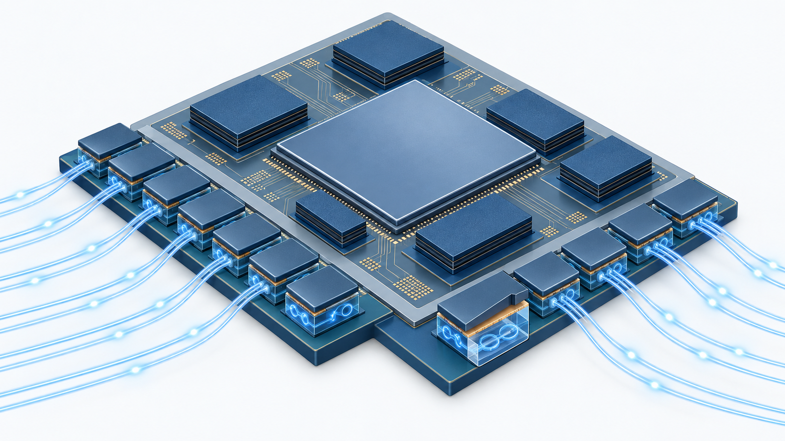
The foundry that has stepped into contract manufacturing of optical interconnect with COUPE, which stacks an electronic chip on a photonic one
TSMC sells no optical modules or optical components under its own brand. Its name still comes up in optical communications because it owns COUPE, a manufacturing technology that combines optical and electrical circuits into a single engine, and in April 2026 it announced that a co-packaged optics (CPO) solution using COUPE on substrate would begin production in 2026. At its July 2026 earnings conference the chairman and CEO said: "We started the production right now, and it will be ramped up." This profile confines the company-wide figures to a single table and sets out what TSMC makes in optics, whom it works with and how far it has got, using only TSMC's own official announcements, annual report and earnings conference, together with its partners' official announcements.
- TSMC in 30 seconds, and where it stands in optical communications and photonics
- The logo and how the name is written
- Where the company sits in optical communications and photonics
- Scale (the company as a whole, in brief)
- Resources committed to optical communications and photonics
- Track record so far
- Plans ahead
- What the company is aiming for in optical communications and photonics
- Partnership map
- Technologies, products and services
- The risks this company carries
- Glossary, references and claim-to-source audit
1. TSMC in 30 seconds, and where it stands in optical communications and photonics
Manufacturing Company LimitedIt also has a Chinese-language name; this article uses TSMC throughout
NYSE: TSMTraded in the U.S. as ADRs
inside the data centrePlacing the optical input and output right next to switches and AI chips
(with several customers)Stated in the 2025 Annual Report. Test conditions not disclosed
(CPO on substrate)Announced April 2026; "started the production" said in July
Companies involved in optical communications fall into three broad types: optical components & modules, chips & foundries, and network systems & carriers. TSMC belongs to chips & foundries, and it handles light inside the data centre, specifically right beside the packages of switches and AI chips Sourced. It has nothing to do with long-haul networks or with optical fibre itself.
What TSMC provides is "a manufacturing process that stacks a photonic chip (PIC) and an electronic chip (EIC) into a single engine"; the design and sale of the optical engine are done by its customers. The 2025 Annual Report says the optical engine achieved "200 Gbps with several customers", but does not name them. Compared with Lumentum or InnoLight, which sell optical modules under their own brands, TSMC occupies a completely different position, even though all three are "optics companies".
2. The logo and how the name is written

The TSMC logo is a trademark of the company. We have not recreated it with generated imagery;
the image was taken from TSMC's official website and is placed here as img/tsmc_logo.png (served as WebP and converted to PNG).
A note on names: the legal name is Taiwan Semiconductor Manufacturing Company Limited, and the company also has a Chinese-language name. The logo uses lower-case "tsmc", but this article follows common usage and writes TSMC in capitals throughout. "COUPE" is a registered trademark of TSMC, short for Compact Universal Photonic Engine, and official documents also write it as "TSMC-COUPE™".
Official site: https://www.tsmc.com/english3. Where the company sits in optical communications and photonics
Within the same "chips & foundries" box, NVIDIA and Broadcom own the products where the light ends up, switches and GPUs. TSMC is the one that manufactures those products; the end products belong to its customers. TSMC's optics business is therefore directly governed by how quickly its customers adopt CPO Not yet confirmed. The idea of bringing optical signals right up to the electronic chip is covered in our explainers on co-packaged optics and on optical interconnect and SerDes.
4. Scale (the company as a whole, in brief)
The company as a whole is not the subject here, so we note only its size Sourced.
| Measure (NT$ million) | FY2023 | FY2024 | FY2025 |
|---|---|---|---|
| Net revenue | 2,161,736 | 2,894,308 | 3,809,054 |
| R&D expense | 182,370 | 204,182 | 246,427 |
| R&D as a share of revenue | 8.5% | 7.1% | 6.5% |
| Regular employees (31 December) | 76,478 | 83,825 | 90,557 |
The figures above are for the whole company. They do not show the size of any optical communications or photonics business. TSMC discloses none of its optics-related revenue, investment or dedicated headcount Not yet confirmed. The Form 20-F for FY2025 (the annual report filed with the U.S. SEC) contains no mention of silicon photonics or COUPE at all. Its optics work is described in the annual report for Taiwanese shareholders (English edition) and in technology symposium announcements. At the July 2026 earnings conference, too, an analyst asked when COUPE would make a meaningful contribution to revenue, and the CEO gave neither a date nor an amount.
5. Resources committed to optical communications and photonics
Amounts and headcounts are not disclosed, but what the company is putting in can be read from the annual report and official announcements. As a matter of method, we always checked four things: people, money, external investment, and universities or public funding.
| Resource | Details | Category |
|---|---|---|
| People (dedicated teams and staff) | No dedicated optics organisation or headcount is stated. The annual report says COUPE is handled by corporate centralised R&D, as one of its 3D integration technologies alongside SoIC, CoWoS and SoW | Not disclosed |
| Money (R&D) | NT$246.4 billion company-wide (2025). The table of major R&D projects for 2026 has six items, "2nm", "A16", "A14 and beyond", "3DIC", "next-generation lithography" and "long-term research", and optics is not a separate item | Sourced |
| Money (line investment) | Capital spending on COUPE and CPO | Not disclosed |
| Investments, acquisitions and joint ventures | No optics-related investments, acquisitions or joint ventures appear in the annual report, the 20-F or official announcements | Could not be confirmed |
| Universities and research institutes | The annual report mentions long-standing partnerships with SRC in the United States and IMEC in Belgium, but these are not specific to optics | Sourced |
| Public funding | No award of government funding for optics R&D (in Taiwan, under the U.S. CHIPS Act or elsewhere) appears in the materials reviewed | Could not be confirmed |
| Design ecosystem | COUPE is supported through the Open Innovation Platform (OIP), TSMC's framework with design tool vendors. In April 2024 Ansys announced a collaboration with TSMC on design and analysis software for COUPE | Sourced |
| Research on light-receiving devices | The annual report says it is developing an avalanche photodiode (APD) with a 7 µm pixel pitch for optical I/O, and has confirmed operation above 2 GHz with low power consumption | Sourced |
TSMC says about 89% of its R&D budget goes to the six items above Sourced. COUPE is a 3D integration technology, so we think it is most likely included under "3DIC", but the company does not say so Not yet confirmed. Either way, no budget set aside for optics alone can be read from outside.
6. Track record so far
| When | What happened | What it means |
|---|---|---|
| 2021 | TSMC researchers propose the COUPE (COmpact Universal Photonic Engine) structure in a paper. It stacks the photonic and electronic chips, achieves low insertion loss with either grating or edge coupling, and is described as having no voids or mechanically weak points | The name and concept of COUPE are first made public, on TSMC's research site |
| April 2024 | Announces COUPE development at the North America Technology Symposium, with a plan to "qualify COUPE for small form factor pluggables in 2025" and integrate it into CoWoS as CPO in 2026 | The first official announcement of optics as a product plan |
| April 2024 | Ansys announces a collaboration with TSMC on multiphysics analysis for COUPE (optical input and output, photonic circuits, power, electromagnetics and thermal) | Preparations for volume production begin on the design tool side |
| March 2025 | NVIDIA announces its CPO switches (Spectrum-X Photonics and Quantum-X Photonics). Its headline cites "Joint Inventions and Collaborations With TSMC" and others, and TSMC's CEO comments that the solution combines TSMC's chip manufacturing with SoIC 3D chip stacking | The first large outlet becomes public |
| April 2025 | At the North America Technology Symposium, presents "silicon photonics integration with TSMC's Compact Universal Photonic Engine (COUPE)" as one of the solutions complementing its logic technology | Now presented alongside its mainstream logic and packaging |
| September 2025 | Alchip and Ayar Labs announce a partnership on CPO using TSMC technologies including COUPE and SoIC, and show a scale model at TSMC's OIP forum the same month | A company other than NVIDIA publicly states it will use COUPE |
| 2025 | According to the annual report, the COUPE optical engine achieved 200 Gbps with several customers, and the COUPE service is on track for volume production in 2026 | Performance confirmed with several customers (the report does not say whether these are volume products) |
| April 2026 | At the North America Technology Symposium, announces "a true co-packaged optics solution using COUPE on substrate beginning production in 2026". Compared with pluggables on board, it offers 2x power efficiency and 10x lower latency, and is featured in a 200 Gbps micro-ring modulator | Names the year volume production begins |
| July 2026 | At the second-quarter earnings conference, Chairman and CEO C.C. Wei says: "We started the production right now, and it will be ramped up", adding that COUPE "will become a fairly important technology in the next few years" | The chief executive confirms verbally that production has begun |
The 2024 announcement planned to "qualify COUPE for small form factor pluggables in 2025", but we could not confirm from later official materials whether that qualification was completed Not yet confirmed. And while the 2024 plan had CPO in 2026 as "integration into CoWoS", what was announced as starting production in April 2026 is CPO "on substrate". The annual report says CPO for switches, which combines CoWoS and COUPE in one package, is "under development" Sourced. The accurate reading is that what began in 2026 is not the whole plan, but the form that was easier to achieve first.
7. Plans ahead
in 2028Not optics, but a larger platform on which CPO would sit
TSMC has announced that a 5.5-reticle CoWoS is now in production, with a 14-reticle version to follow in 2028 and larger ones in 2029 Sourced. CPO integrated with CoWoS would place the optical input and output on top of this platform, so the plan to enlarge packages and the plan for optics can be read as lying on the same path Not yet confirmed.
None of the following appears in TSMC's official materials Not yet confirmed.
COUPE and CPO revenue and its share of the total / production capacity (wafers per month and so on) / production sites / optics-related capital spending / the names of customers that achieved 200 Gbps (other than NVIDIA) / the year volume production starts for CPO integrated with CoWoS / who supplies the light source (laser). Figures of the "TSMC's silicon photonics revenue will reach US$X in year Y" kind come from research firms or press reports, and this article does not use them.
8. What the company is aiming for in optical communications and photonics
This section includes things the company does not say directly. We set them out as inferences within what the primary sources support, with the evidence for each.
| What the evidence suggests | Primary information it rests on | Category |
|---|---|---|
| Optics is sold not as a standalone business but as part of its 3D integration services (3DFabric) | The annual report places COUPE within "3DFabric" alongside SoIC, CoWoS and SoW. No separate optics business unit is mentioned | Sourced |
| The aim is to bring light right inside the AI chip's package | The annual report says the optical engine can be co-packaged with HPC chips, and that CPO for switches integrated with CoWoS is under development | Inference |
| For now, the main outlet is NVIDIA's CPO switches | The only customer named in primary sources is NVIDIA, in NVIDIA's own announcement. The annual report says "several customers" but gives no names | Inference |
| It positions itself not to compete with optical module makers but to manufacture for them too | Companies that design their own optical I/O, such as Alchip and Ayar Labs, have announced they will use COUPE. Nothing says TSMC itself will sell optical modules | Inference |
| It intends to grow COUPE into a key technology over several years | The CEO said at the earnings conference that it "will become a fairly important technology in the next few years". No revenue target was given | Sourced |
TSMC consistently describes optics not as "optical technology" but as an application of its chip-stacking technology. The 2024 announcement says COUPE uses SoIC-X to stack the electrical die on top of the photonic die, and the 2025 Annual Report says the COUPE service uses SoIC chip-on-wafer (CoW) stacking to integrate the silicon photonics chip with the electrical control chip Sourced. The CEO's comment in NVIDIA's announcement likewise spoke of combining cutting-edge chip manufacturing with TSMC-SoIC 3D chip stacking. Lasers and optical fibre appear in none of these materials. From this we read that TSMC's winning formula rests not on competing on optical device performance but on stacking and packaging yield and volume capacity Not yet confirmed.
9. Partnership map
10. Technologies, products and services
The optics-related technologies TSMC has disclosed are three: COUPE (stacked optical engines), CPO built with COUPE and light-receiving devices (APDs). Nothing is said about light-emitting devices (lasers).
| Item | What the official materials say | In production or in development |
|---|---|---|
| COUPE structure | Uses SoIC-X chip stacking to stack the electrical die on top of the photonic die. Described as offering the lowest die-to-die impedance and higher energy efficiency than conventional stacking methods | Production started 2026 |
| COUPE performance | As an optical engine, achieved 200 Gbps with several customers (2025). Number of lanes and reach not disclosed | Stated as achieved with several customers (whether in volume products is unclear) |
| CPO on substrate | Putting the optical engine in the package gives 2x power efficiency and 10x lower latency compared with pluggables on board (company claim). Featured in a 200 Gbps micro-ring modulator | Production started 2026 |
| CPO integrated with CoWoS | Combines an interposer-based CoW module and COUPE-based optical I/O in one package. For ultra-high-end network switches | In development |
| Light-receiving devices | An avalanche photodiode with a 7 µm pixel pitch for optical I/O, stated to meet industry requirements with operation above 2 GHz and very low power. Separately, a Ge/Si single-photon avalanche diode (SPAD) with dark count rate cut by about a factor of ten (presented at IEDM 2025) | In development |
| Design support | Design and analysis flows for COUPE through OIP, TSMC's framework with design tool vendors. Ansys says its Lumerical (photonic circuit simulator) circuit models were co-designed with TSMC's PDK (the set of process information used for design) | Available |
"2x power efficiency and 10x lower latency" is a comparison TSMC itself made, and the conditions (reach, lane count, generation of the pluggable product compared) have not been published Sourced. Nor did the official materials we reviewed say anything about compliance with standards such as IEEE 802.3 or OIF specifications Not yet confirmed. For the basics of micro-ring modulators and photodetectors, see our explainers on wavelength multiplexing and micro-rings, on photodetectors and on silicon photonics.
The essence of COUPE is that the electrical and photonic dies are stacked directly with SoIC bonding rather than with solder bumps Sourced. The shorter the distance between the modulator and the circuit that drives it, the lower the parasitic capacitance of the wiring and the less energy it takes to send each bit. That is the point TSMC stresses when it says the die-to-die impedance is the lowest.
From the materials and thermal side, however, the difficulties multiply. A micro-ring modulator's resonant wavelength shifts with even a small change in temperature, so in a structure that places a heat-generating electronic chip directly above it, thermal management decides whether the product succeeds Not yet confirmed. That the Ansys collaboration covered thermal analysis as well as optical input and output and power, and that TSMC's 2021 paper stressed a structure with no voids or mechanically weak points, can be read as recognition that the reliability of the stack and its bonded interfaces is the key to volume production.
11. The risks this company carries
| Risk | Details | Category |
|---|---|---|
| Progress cannot be verified from outside | Optics-related revenue, capacity, investment and customer numbers are all undisclosed. The CEO did not give a date for a revenue contribution either | Sourced |
| The shape of the plan has changed | The 2024 plan was "CPO integrated into CoWoS in 2026", but what started production in 2026 is CPO on substrate. The CoWoS-integrated form remains in development | Sourced |
| Dependence on customers' adoption pace | TSMC does not own the outlets for light (switches and GPUs). How fast CPO replaces pluggables is decided by its customers and, beyond them, by data centre operators | Inference |
| Skew towards one customer | The only large optics customer named in primary sources is NVIDIA. The annual report mentions several customers but does not name them | Inference |
| No light source of its own | The official materials say nothing about lasers. The light source appears to depend on customers' or other companies' components, so part of CPO's reliability and serviceability is determined outside TSMC | Inference |
| Thermal and bonding reliability | The structure places temperature-sensitive optical devices under a heat-generating chip, so the reliability of the stacked interfaces feeds straight into yield | Inference |
| Competition from other foundries | GlobalFoundries, Tower Semiconductor and UMC, all covered in this series, have also officially put forward silicon photonics foundry services | Our calculation |
12. Glossary
- COUPE
- Compact Universal Photonic Engine: TSMC's optical engine technology, which stacks an electronic chip on a photonic chip to form one engine.
- CPO (co-packaged optics)
- Placing the optical transmit and receive functions inside the same package as a switch or AI chip. The wiring is shorter than with pluggable modules on the board.
- PIC / EIC
- A PIC is a chip with optical circuits built in; an EIC is a chip with electrical circuits (driving modulators and amplifying received signals).
- SoIC
- TSMC's chip-stacking technology, which joins chips directly with fine-pitch bonds and stacks them vertically.
- CoWoS
- TSMC's 2.5D packaging technology, which places AI chips and HBM side by side on a large intermediate substrate (interposer).
- Micro-ring modulator
- A device that switches light on and off with an electrical signal using a ring-shaped light path thinner than a hair. Small and low-power but sensitive to temperature.
- APD
- Avalanche photodiode: a light-receiving device that amplifies the received light internally as it converts it into an electrical signal.
- OIP
- Open Innovation Platform: TSMC's framework for supporting customer designs together with design tool and IP vendors.
13. References
- TSMC Press release, "TSMC Debuts A13 Technology at 2026 North America Technology Symposium" (issued 23 April 2026). Production of CPO using COUPE on substrate from 2026, 2x power efficiency and 10x lower latency, the 200 Gbps micro-ring modulator, and plans for larger CoWoS. https://pr.tsmc.com/english/news/3302
- TSMC Press release, "TSMC Unveils Next-Generation A14 Process at North America Technology Symposium" (issued 24 April 2025). Presentation of silicon photonics integration with COUPE. https://pr.tsmc.com/english/news/3228
- TSMC Press release, "TSMC Celebrates 30th North America Technology Symposium with Innovations Powering AI with Silicon Leadership" (issued 24 April 2024). The COUPE structure (SoIC-X stacking the electrical die on the photonic die) and the plan for pluggable qualification in 2025 and CoWoS-integrated CPO in 2026. https://pr.tsmc.com/english/news/3136
- TSMC 2025 Annual Report, chapter 5 (operations). COUPE reaching 200 Gbps and the 2026 volume production plan, development of CoWoS-integrated CPO, APDs and SPADs, R&D expenditure, major R&D projects and partnerships with SRC and IMEC. https://investor.tsmc.com/static/annualReports/2025/english/pdf/2025_tsmc_ar_e_ch5.pdf
- TSMC Form 20-F for the fiscal year ended December 31, 2025 (filed with the U.S. SEC). Net revenue, R&D expense, R&D as a share of revenue and regular headcount. https://www.sec.gov/Archives/edgar/data/1046179/000162828026025362/tsm-20251231.htm
- TSMC Transcript of the second-quarter 2026 earnings conference (held 16 July 2026; edited transcript prepared by LSEG and published by TSMC on its investor site). Comments by Chairman and CEO C.C. Wei on the start of COUPE production and its outlook. https://investor.tsmc.com/english/encrypt/files/encrypt_file/reports/2026-08/3e494f0c14dd0890f897aa044415e21d93486cc4/TSMC%202Q26%20Transcript.pdf
- TSMC Research site, "Heterogeneous Integration of a Compact Universal Photonic Engine for Silicon Photonics Applications in HPC" (page presenting a 2021 paper). The proposal of COUPE and its structural features. https://research.tsmc.com/page/on-chip-interconnect/14.html
- NVIDIA Press release, "NVIDIA Announces Spectrum-X Photonics, Co-Packaged Optics Networking Switches to Scale AI Factories to Millions of GPUs" (18 March 2025). Joint inventions and collaboration with TSMC and others, a comment from TSMC's CEO, and product availability. https://nvidianews.nvidia.com/news/nvidia-spectrum-x-co-packaged-optics-networking-switches-ai-factories
- Ansys Press release, "Ansys and TSMC Enable a Multiphysics Platform for Optics and Photonics" (24 April 2024). Collaboration on multiphysics analysis for COUPE and a comment from the head of TSMC's design infrastructure management division. https://ansys.synopsys.com/news-center/press-releases/4-24-24-ansys-collaborates-with-tsmc-coupe-on-multiphysics
- Alchip Technologies Press release, "Ayar Labs and Alchip to Scale AI Infrastructure with Co-Packaged Optics" (8 September 2025). Partnership on CPO using TSMC's COUPE, SoIC and other technologies. https://www.alchip.com/en/Newsroom/AyarLabsandAlchiptoScaleAIInfrastructure
- Alchip Technologies Press release, "Alchip and Ayar Labs Unveil Co-Packaged Optics for AI Datacenter Scale-Up" (26 September 2025). A scale model of the CPO solution shown at the 2025 TSMC North America OIP Ecosystem Forum. https://www.alchip.com/en/Newsroom/AlchipandAyarLabsUnveilCPOforAIDatacenterScale-Up
- TSMC Official website (source of the company name style and the logo image). https://www.tsmc.com/english
14. Claim-to-source audit
| Claim in the article | Category | Source |
|---|---|---|
| Legal name, listing venues, net revenue, R&D expense, R&D ratio and regular headcount (2023 to 2025) | Sourced | Reference 5 https://www.sec.gov/Archives/edgar/data/1046179/000162828026025362/tsm-20251231.htm |
| 2025 R&D expenditure of NT$246,427,264 thousand; about 89% going to six major R&D projects; optics not a separate item | Sourced | Reference 4 https://investor.tsmc.com/static/annualReports/2025/english/pdf/2025_tsmc_ar_e_ch5.pdf |
| No mention of silicon photonics or COUPE in the 20-F | Sourced | Reference 5 (confirmed by this article's full-text search) https://www.sec.gov/Archives/edgar/data/1046179/000162828026025362/tsm-20251231.htm |
| COUPE stacks the electrical die on the photonic die using SoIC-X, with the lowest die-to-die impedance | Sourced | Reference 3 https://pr.tsmc.com/english/news/3136 |
| The 2024 plan (pluggable qualification in 2025, CoWoS-integrated CPO in 2026) | Sourced | Reference 3 https://pr.tsmc.com/english/news/3136 |
| Presentation of silicon photonics integration with COUPE at the 2025 symposium | Sourced | Reference 2 https://pr.tsmc.com/english/news/3228 |
| The COUPE optical engine achieved 200 Gbps with several customers (2025), volume production planned for 2026, CoWoS-integrated CPO for switches under development | Sourced | Reference 4 https://investor.tsmc.com/static/annualReports/2025/english/pdf/2025_tsmc_ar_e_ch5.pdf |
| COUPE is part of 3DFabric and handled by corporate centralised R&D; partnerships with SRC and IMEC | Sourced | Reference 4 https://investor.tsmc.com/static/annualReports/2025/english/pdf/2025_tsmc_ar_e_ch5.pdf |
| APD for optical I/O (7 µm, above 2 GHz) and Ge/Si SPAD with dark count rate cut by about ten times | Sourced | Reference 4 https://investor.tsmc.com/static/annualReports/2025/english/pdf/2025_tsmc_ar_e_ch5.pdf |
| Production of CPO on substrate from 2026, 2x power efficiency and 10x lower latency, 200 Gbps micro-ring modulator | Sourced | Reference 1 https://pr.tsmc.com/english/news/3302 |
| 5.5-reticle CoWoS in production, 14-reticle version in 2028 and larger ones in 2029 | Sourced | Reference 1 https://pr.tsmc.com/english/news/3302 |
| The CEO's remarks "We started the production right now" and "a fairly important technology in the next few years", and his not giving a date for a revenue contribution | Sourced | Reference 6 https://investor.tsmc.com/english/encrypt/files/encrypt_file/reports/2026-08/3e494f0c14dd0890f897aa044415e21d93486cc4/TSMC%202Q26%20Transcript.pdf |
| COUPE proposed in a 2021 paper and described as a low-insertion-loss structure without voids | Sourced | Reference 7 https://research.tsmc.com/page/on-chip-interconnect/14.html |
| Joint inventions and collaboration with TSMC on NVIDIA's CPO switches, and the comment from TSMC's CEO | Sourced | Reference 8 https://nvidianews.nvidia.com/news/nvidia-spectrum-x-co-packaged-optics-networking-switches-ai-factories |
| Collaboration with Ansys on multiphysics analysis for COUPE (including thermal), and co-design of Lumerical models with the PDK | Sourced | Reference 9 https://ansys.synopsys.com/news-center/press-releases/4-24-24-ansys-collaborates-with-tsmc-coupe-on-multiphysics |
| Alchip and Ayar Labs partner on CPO using COUPE and SoIC and show a model at the OIP forum | Sourced | References 10 and 11 https://www.alchip.com/en/Newsroom/AyarLabsandAlchiptoScaleAIInfrastructure |
| The three types of optical communications company | Our calculation | Our own classification. Example companies drawn from those covered in this series |
| Optics-related revenue, capacity, production sites, capital spending, dedicated staff, customer names (other than NVIDIA), and the supplier of the light source | Not yet confirmed | Not stated in references 1 to 6. Research-firm and press figures are not used https://investor.tsmc.com/static/annualReports/2025/english/pdf/2025_tsmc_ar_e_ch5.pdf |
| Whether the 2025 pluggable qualification was completed | Not yet confirmed | Not stated in references 1, 2 and 4. This article does not conclude either way https://pr.tsmc.com/english/news/3302 |
| Optics-related investments, acquisitions and joint ventures; public funding specific to optics | Not yet confirmed | Not stated in references 4 and 5. This article does not conclude that they do not exist either https://www.sec.gov/Archives/edgar/data/1046179/000162828026025362/tsm-20251231.htm |
| Compliance with standards (IEEE 802.3, OIF and others) | Not yet confirmed | Not stated in references 1 to 4 https://pr.tsmc.com/english/news/3302 |
| The reading that the COUPE budget is most likely included under "3DIC" | Inference | This article's interpretation of the table of major R&D projects |
| The reading that 2026 production is part of the plan, starting with the form easier to achieve | Inference | This article's interpretation from comparing the plan in reference 3 with references 1 and 4 |
| The reading that the package-enlargement plan and the optics plan lie on the same path | Inference | This article's interpretation of references 1 and 4 |
| The readings that the aim is to bring light inside the AI chip package, that NVIDIA is the main outlet for now, and that TSMC positions itself to manufacture for optical module makers too | Inference | This article's interpretation of references 4, 8 and 10 |
| The reading that its winning formula lies in stacking and packaging volume capacity rather than optical device performance | Inference | This article's interpretation of what references 3, 4 and 8 have in common |
| The temperature sensitivity of micro-rings and the difficulty of thermal management when stacking a heat-generating chip | Inference | This article's commentary based on the general properties of such devices. Not something TSMC has stated |
| The risks of dependence on customers' adoption pace, skew towards one customer, having no light source, and thermal and bonding reliability | Inference | This article's interpretation of the partnership structure and published information |
| Other foundries also putting forward silicon photonics foundry services | Our calculation | Our own summary, based on the profiles of each company in this series |
Last updated 25 September 2026 / Troy Technical
Every figure in this article comes from TSMC's official announcements, annual report, U.S. SEC filing and earnings conference transcript, and from its partners' official announcements. No research-firm estimates or press-based figures have been used. Passages marked "Inference" are this article's interpretation of the primary sources, not statements made by the company.