TECHNOLOGY EXPLAINER
Photonic Integrated Circuits and Indium Phosphide
— building the whole circuit into a crystal that emits light
A photonic integrated circuit (PIC) gathers optical components onto a single chip, and there are several materials it can be built on. Among them, indium phosphide (InP) is the one on which lasers, amplifiers, modulators and detectors can all be made in the same crystal. The price is a process step in which the crystal is etched away and regrown with a different composition, and wafers that top out at 150 mm. Two things are happening at once today: InP wafers are getting bigger, and InP is being bonded onto silicon.
- Photonic integrated circuits and InP in three points
- Three ways to build one — grow it in one crystal, bond it, or place it alongside
- Inside monolithic integration — etch away, then regrow
- A materials engineer's view (1): small substrates, with dislocations
- Our calculation: the doped layer sets the loss
- Heterogeneous integration — bonding InP onto silicon
- A materials engineer's view (2): bonding is a problem of surfaces and heat
- Comparing the material platforms
- What is still hard
- Glossary / References / Claim-to-source audit
Sourced = stated in published material or a peer-reviewed paper (link given)
Our calculation = a figure this article derived, with the assumptions spelled out
Not yet confirmed = a plan, target or research-stage result with no confirmed production record
Structural readings and materials-design interpretations are marked separately as Commentary.
Where a company describes something as a “world first” or similar, we treat it as that company's claim.
1. Photonic integrated circuits and InP in three points
A photonic integrated circuit (PIC) puts the path light travels along (the waveguide), the parts that amplify light, the parts that put a signal onto it and the parts that turn it back into electricity together on a single chip. Indium phosphide (InP) is one of the compound semiconductor crystals such a chip can be built on.
- What it can do: InP-based materials emit light. Smit and colleagues at TU Eindhoven explain that in InP generic integration technology, optical amplifiers (SOAs), phase modulators and polarisation converters give control over the amplitude, phase and polarisation of light, and that lasers, modulators and even switches can be assembled from theseSourced
- What makes it hard: the section that emits light and the section that only carries it need different crystal compositions. So a step is needed to make different compositions in different parts of the crystalSourced
- What is happening now: a move to larger InP wafers (Coherent's shift to 6 inch) and a move to bond InP onto silicon (heterogeneous integration) are running in parallelSourced
Photonic circuits built on silicon (waveguides, modulators, Ge detectors, couplers) were covered in our explainer on silicon photonics, and the reasons for placing the light source outside the package in our explainer on co-packaged optics. This article covers what changes when the foundation is InP, a crystal that can emit light, and how InP is brought onto silicon. The structure of the lasers themselves (DFB, EML, VCSEL) is covered in our explainer on semiconductor lasers, and detector materials in our explainer on photodetectors.
2. Three ways to build one — grow it in one crystal, bond it, or place it alongside
There are three broad ways to bring optical components together on one chip (or in one package). A 2024 Nature Communications paper by Shekhar and colleagues sorts the ways of adding a laser to a silicon photonic circuit into hybrid (a separate chip placed alongside or on top), heterogeneous (bonded by direct bonding or transfer) and monolithic (grown directly by heteroepitaxy)Sourced. Building everything on an InP substrate from the start is called InP monolithic integration.
| Approach | What it involves | What the primary sources say |
|---|---|---|
| InP monolithic | Everything is built on an InP substrate, with light-emitting and passive layers made separately | The JePPIX roadmap describes integration platforms as the basis for integrating “lasers, amplifiers, modulators, detectors and interferometers” on one chipSourced |
| Heterogeneous | InP-based layers are bonded to a silicon wafer and processed at wafer level | Shekhar et al. describe it as one of the approaches that has been commercially successful in HVM (>million/year)Sourced |
| Hybrid | Finished laser chips and the like are made separately, then placed alongside or on top | Shekhar et al. describe as “commercially successful” the 2.5D approach of mounting known-good lasers with epoxy, ball lenses and isolatorsSourced |
| Monolithic (grown on Si) | III-V crystal is grown directly on silicon | Shekhar et al.: it “remains the end goal”. Holland et al. (2017): it has been researched for more than 30 years, but defects, cost and complexity have kept it from large-scale commercialisationSourced |
Sources: JePPIX roadmap [Reference 2], Shekhar et al. [Reference 7], Holland et al. [Reference 9]. The grouping and the “What it involves” column are this article's summary.
3. Inside monolithic integration — etch away, then regrow
The heart of InP monolithic integration is how to join the section that emits light to the section that only carries it. A section that emits light at a given wavelength also absorbs it. If the passive section kept the same composition, the light would simply be absorbed and lost. Smit and colleagues list four ways of combining active (amplifying) and passive (transparent waveguide) sections on one chip: vertical twin-guide, vertical single-guide, quantum well intermixing (QWI) together with selective area growth (SAG), and butt-joint integrationSourced.
The most common method: butt-joint regrowth
Smit and colleagues call butt-joint integration “the most frequently applied approach”Sourced. It takes three growth steps.
Smit and colleagues note that because the active and passive sections are made in separate growth steps, the approach offers a great deal of freedom in layer structure and doping, and write that “In the past the additional growth steps could cause serious yield problems, however, with modern epitaxial technology this is no longer an issue.”Sourced
The standard waveguide in the same paper is a 0.5 µm layer of Q1.25. Q1.25 is explained as quaternary InGaAsP with a composition that puts the band edge at 1.25 µm, lattice-matched to the InP substrateSourced. Light in the 1.55 µm band passes through a layer with a 1.25 µm band edge without being absorbed (our commentary).
The other route: shifting the composition place by place
There are also methods that avoid etching and regrowing altogether and instead vary the bandgap from place to place across the wafer.
- Selective area growth (SAG): during MOVPE growth, masking both sides of the active region makes the source species on the mask migrate sideways, so that the active region grows faster, the quantum wells come out thicker and the bandgap drops. It is controlled through mask width and gap, and each active region can reportedly be tuned individually over a range of about 100 nmSourced
- Quantum well intermixing (QWI): covering the crystal with a material that generates vacancies and then heating it drives the vacancies down into the active layer, so that the atoms of well and barrier intermix and the bandgap widens. The shift can exceed 100 nm, enough to make the material fully transparent, and intermediate values can be used for electro-absorption modulatorsSourced
In silicon photonics, waveguides and modulators are both made by processing the same silicon layer, and the one missing function, detection, is added with selectively grown Ge (see our explainer on silicon photonics). InP monolithic integration works the other way round. Functions are separated by changing the composition of the crystal itself from place to place on a single substrate.
- Butt joint: a lattice-matched layer of a different composition is regrown sideways, flush into the etched step. The shape of the junction and the cleanliness of the interface determine reflection and loss
- SAG: a layout dimension, the mask width, turns into bandgap by way of growth rate. Diffusion in the gas phase, a transport phenomenon, becomes a design parameter
- QWI: point defects (vacancies) are deliberately injected and made to diffuse. A phenomenon one would normally try to avoid is put to work as a process
Each of these steps can be described in the vocabulary of materials technology: crystal growth, thin films and diffusion. Many of the variables that set the performance of the photonic circuit sit in growth conditions and interfaces — and that is what characterises InP as a foundation (our commentary).
4. A materials engineer's view (1): small substrates, with dislocations
InP's biggest weakness is not performance but the substrate. Sumitomo Electric Industries, a major InP substrate supplier, publishes standard specifications for its n-type InP substratesSourced.
| Diameter | Thickness | EPD (average) | Growth method, dopant |
|---|---|---|---|
| 50.0 mm (2 inch) | 350 ± 15 µm | ≤ 5×10² cm⁻² | VB, S |
| 76.0 mm (3 inch) | 600 ± 15 µm | ≤ 5×10³ cm⁻² | VB, S |
| 100.0 mm (4 inch) | 625 ± 25 µm | ≤ 5×10³ cm⁻² | VB, S |
| 150.0 mm (6 inch) | 675 ± 25 µm | ≤ 1×10⁴ cm⁻² | VB, S |
Sourced (Sumitomo Electric Industries, standard specifications for n-type InP substrates [Reference 4]). EPD is etch pit density, a proxy for the density of dislocations in the crystal. VB is Vertical Boat, per the company. The inch designations are our addition. The same table also lists a Sn-doped (2 inch) specification.
The company also publishes Fe-doped semi-insulating InP substrates in the same four sizes: Fe concentration ≥ 0.3 wtppm, resistivity ≥ 1×10⁷ Ω·cm, and EPD ≤ 5×10³ cm⁻² up to 4 inch and ≤ 10×10³ cm⁻² at 6 inchSourced. Smit and colleagues note that Fraunhofer HHI's InP integration process uses semi-insulating (Fe-doped) substrates, giving better RF capability and electrical isolation between devicesSourced.
Converting from the published valuesOur calculation:
- Area: 76.0 mm diameter → about 45.4 cm²; 150 mm → about 176.7 cm². A ratio of about 3.9
- The gap to silicon: 300 mm (about 706.9 cm²) is 4.0 times 150 mm, 9.0 times 100 mm and 15.6 times 76.0 mm
- Dislocations, roughly: EPD 5×10³ cm⁻² ÷ 100 mm²/cm² = an average of 50 per mm². At the 6 inch upper limit of 1×10⁴ cm⁻², 100
Assumptions and limits: EPD figures are specification upper limits; actual values may be lower. How far substrate dislocations propagate into the epitaxial layers, and how much they affect device characteristics and lifetime, depends on layer structure and device type, and could not be confirmed quantitatively in the primary sources this article consulted. The area ratios are ratios of circle areas and ignore edge exclusion and how dies are laid out.
The move to 6 inch
On 25 March 2024 Coherent announced that it had established 6-inch InP wafer manufacturing capability at its fabs in Sherman, Texas, and Järfälla, Sweden, describing it as the “world's first” (the company's claim)Sourced. The company says 6-inch wafers will deliver “4x the number of devices per wafer” and a “greater than 60% reduction in die cost”, and that it is qualifying 200G EMLs, 200G DFB-MZ lasers, 100G EMLs, high-speed photodetectors and high-power CW lasers for silicon photonics on 6 inchSourced. Moving the bulk of production from 3 inch to 6 inch is a plan for “the next few years”Not yet confirmed.
Intel, for its part, announced in June 2022 as a research result an eight-wavelength DFB laser array built on a 300 mm hybrid silicon photonics platform, saying its wavelength uniformity was better than that of conventional semiconductor lasers made in “3-inch or 4-inch III-V wafer fabs”Sourced. The company explains that the gratings were defined lithographically in the silicon first, and the III-V wafer bonded on afterwardsSourced.
What stands out in the Sumitomo Electric specification table is that the EPD ceiling loosens as the diameter grows. Against ≤ 5×10² cm⁻² at 2 inch, the 6 inch figure is ≤ 1×10⁴ cm⁻² — 20 times higher at the limitOur calculation (1×10⁴ ÷ 5×10² = 20).
That says InP is a material in which growing large-diameter crystals with low dislocation density is genuinely difficult. And what gets built on it is a laser, one of the device classes most sensitive to crystal defects (our commentary).
Coherent's “3 inch to 6 inch” and Intel's “more uniform than 3- and 4-inch III-V fabs” are in the end two views of the same fact: the small size of InP substrates constrains the cost and uniformity of optical components. Moving to 6 inch means reworking conditions across substrates, crystal growth and wafer processing alike, so it is an opportunity in its own right for substrate makers and equipment makers (our commentary).
5. Our calculation: the doped layer sets the loss
InP waveguides are lossier than silicon or silicon nitride waveguides. Smit and colleagues state that the p-doped upper cladding needed to drive current into the active devices adds a loss of the order of 2 dB/cm even with an optimised layer stack, and that removing the p-dopant from the transparent waveguide sections brings it below 1 dB/cmSourced. Fraunhofer HHI's 2018 foundry overview lists “1 dB / cm waveguides” among its specificationsSourced.
A loss of L dB means the optical power is multiplied by 10−L/10Our calculation.
- 2 dB/cm × 3 cm = 6 dB → 10−0.6 = about 25% remains
- 1 dB/cm × 3 cm = 3 dB → 10−0.3 = about 50% remains
- For reference, 0.1 dB/cm × 3 cm = 0.3 dB → about 93% remains (using 0.1 dB/cm, the top of the loss range the JePPIX roadmap gives for silicon nitride technology)
Assumptions and limits: the 3 cm length is our own choice, following Smit et al.'s remark that “larger PICs … may have several centimetres of waveguide length”. Bend, splitter and junction losses are not included.
The reading is that InP can emit light, but in exchange it is poor at carrying light over long distances. The p-type doping needed to drive current into the active devices becomes loss in the passive sections as well — a clash between electrical and optical requirements playing out inside the layer stack (our commentary). The JePPIX roadmap also describes a hybrid example that pairs a low-loss technology such as silicon nitride with InP active devices: a beamforming module for satellite communications and 5G in which three InP PICs are assembled onto a silicon nitride PICSourced. Silicon nitride waveguides are covered in detail in our explainer on silicon nitride waveguides.
6. Heterogeneous integration — bonding InP onto silicon
Silicon is an indirect-bandgap semiconductor and cannot emit light efficiently. As Shekhar and colleagues put it, “Silicon's indirect bandgap prohibits efficient optical gain”Sourced. Heterogeneous integration answers this by bonding InP-based crystal layers onto a silicon wafer and then processing them with wafer-level steps.
- How it is bonded: die-to-die, die-to-wafer or wafer-to-wafer, using direct (molecular) bonding or adhesive bondingSourced
- The advantage of die-to-wafer: known-good dies (KGD) can be used, which raises yieldSourced
- The drawback of wafer-to-wafer: the mismatch in diameter wastes area between the receiving SOI wafer (200 mm or 300 mm) and the source wafer (150 mm or less)Sourced
- Track record: one of the approaches that has been commercially successful in HVM (>million/year). III-V chips are bonded with only coarse alignment and then processed into quantum well lasers on the silicon waferSourced
All from Shekhar et al. (Nature Communications, 2024) [Reference 7].
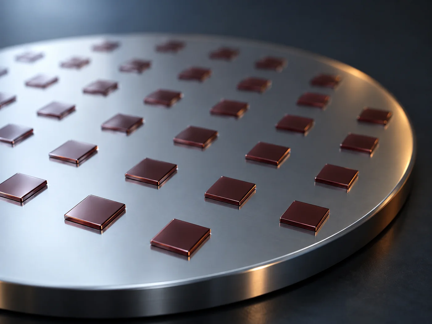
The key point of this approach is that coarse alignment is good enough. In Intel's account, the gratings are first defined lithographically on the silicon side, and the III-V wafer is bonded afterwardsSourced. The precise features that set the wavelength are made in a silicon fab, and InP is supplied as the light-emitting material (our commentary).
The approach has also become a foundry platform. On 11 August 2026 Tower Semiconductor and OpenLight announced that the design kit for Tower's PH18DA “InP-on-silicon” platform had been made available in Cadence design tools. The platform is described as able to integrate lasers, modulators and amplifiers into a single monolithic PIC, and the announcement mentions designs for 400G and 1.6T laser-integrated PICs and for NPO/CPOSourced.
7. A materials engineer's view (2): bonding is a problem of surfaces and heat
Shekhar and colleagues are quite specific about the conditions for direct bondingSourced.
- Surface: very smooth, clean surfaces are needed. CMP (chemical mechanical polishing) is already used in volume production for InP-to-Si direct bonding
- Heat: annealing is needed for strong molecular bonds and for outgassing, but the processed SOI wafer limits the temperature. “Low-temperature” anneals below 350 °C are the norm, which requires proprietary outgassing techniques and bonding conditions
- Expansion: the mismatch in coefficient of thermal expansion (CTE) must be minimised
- With an adhesive layer: surface topography requirements relax and the bond is stronger, but heat dissipation, long-term stability, optical power handling and drift need further study
- In laser operation: care is needed over the buried oxide (BOX) thermally isolating the light-emitting region, and over CTE mismatch
Recast in materials terms, these become three design variables (our framing).
- Interface chemistry: surface smoothness, cleanliness and activation (the paper also mentions O₂ plasma-assisted bonding and covalent direct bonding through SiO₂Sourced)
- A ceiling on thermal history: achieving both outgassing and bond strength below 350 °C
- A way out for heat: the oxide is an insulator both electrically and thermally, so a separate path has to be built to remove heat from the light-emitting layer
The issues raised for adhesive bonding — heat dissipation, long-term stability, optical power handling and drift — line up exactly with the requirements for optical-path adhesives seen in our explainers on co-packaged optics and silicon photonics. In photonics, a bonding layer is judged not as a layer that sticks things together but as a layer that light and heat pass through (our commentary).
There is also work on building that way out for heat from the substrate side. NGK Insulators presents, as a development product, an “InP composite wafer for high-power lasers” in which InP is directly bonded to SiC, a high-thermal-conductivity material, and says its proprietary bonding and polishing technologies can suppress heating in lasers formed on the InP waferSourced (the product is still under developmentNot yet confirmed). The idea is to bond InP not onto silicon but onto a heat-spreading material, which shows bonding technology being used in photonics in two different ways (our commentary).
Direct bonding of InP is in volume production for lasers, but extending it to modulators runs into a different wall. Shekhar and colleagues point out that the optimum bandgap differs for lasers and modulators, which makes heterogeneous integration considerably more complexSourced. The problem of varying the composition from place to place seen in section 3 follows InP into the world of bonding as well (our commentary).
8. Comparing the material platforms
Besides InP, photonic integrated circuits can be built on silicon, silicon nitride, thin-film lithium niobate and other materials. Here are the strengths and weaknesses of each, as the primary sources describe them.
| Platform material | Strengths | Weaknesses and constraints | In this series |
|---|---|---|---|
| InP | Emitting, amplifying, modulating and detecting light, all on one chip. Smit et al. claim InP design kits support more powerful component libraries than silicon photonicsSourced | Substrates top out at 150 mm and carry EPD (Sumitomo Electric specifications). Loss in p-doped sections of about 2 dB/cm (Smit et al.)Sourced | This article |
| Silicon (SOI) | Can be made in 200 mm and 300 mm CMOS fabs. Ge detectors and SiN are offered as standard by several foundries (Shekhar et al.)Sourced | Indirect bandgap, so it cannot emit light efficiently (Shekhar et al.)Sourced | Our explainer on silicon photonics |
| Silicon nitride | A wide wavelength range of roughly 400 nm to 2500 nm, and low loss of 0.1 dB/cm down to 0.1 dB/m (JePPIX)Sourced | Where active devices are needed, it plays a complementary role, combined in hybrid or heterogeneous circuits (JePPIX)Sourced | Our explainer on silicon nitride waveguides |
| Thin-film lithium niobate | Fast modulation through the Pockels effect, with electro-optic bandwidths above 100 GHz (Shekhar et al.)Sourced | Lithium is a contaminant in CMOS fabs, which limits front-end integration (Shekhar et al.)Sourced | Our explainer on thin-film lithium niobate |
Sources: Smit et al. [Reference 1], JePPIX roadmap [Reference 2], Sumitomo Electric Industries [Reference 4], Shekhar et al. [Reference 7]. Setting the four materials side by side in one table is this article's own arrangement, not a ranking.
The JePPIX roadmap (2021) describes “a converged, full-function monolithic platform unlikely for the foreseeable future”Sourced. According to the same roadmap, in 2020 producers of silicon photonic and InP PICs were producing in the order of millions of parts per year in vertically integrated fabsSourced. In other words, InP and silicon are not replacing one another; they coexist as a division of labour between the part that emits light and the part that is made in huge volume (our commentary).
9. What is still hard
(1) Volume production on 6-inch InP is still ahead
Coherent has announced 6-inch InP manufacturing capability, but moving the bulk of production is planned over “the next few years”Not yet confirmed. The “greater than 60%” die-cost reduction is also the company's projection. As of this article's research (September 2026), no primary source could be found showing the yield or cost of volume products on 6-inch InP.
(2) Direct growth on silicon is still the end goal
Shekhar and colleagues say that monolithic integration by heteroepitaxy, without a III-V substrate, “remains the end goal”Not yet confirmed. Holland and colleagues (2017) note that while III-V integration on Si has been researched for more than 30 years, residual defects, high cost and complex integration schemes have kept it from large-scale commercialisationSourced.
(3) Bonding modulators too means reconciling bandgaps
Because lasers and modulators want different bandgaps, Shekhar and colleagues say InP/Si modulators need substantial gains in efficiency and bandwidth before they are widely adoptedSourced. Which approach (InP, thin-film lithium niobate or something else) becomes the next-generation standard is not settledNot yet confirmed.
(4) How substrate dislocations affect device lifetime could not be quantified from public information
A quantitative link between the EPD in section 4 and laser lifetime or yield could not be confirmed in the primary sources this article consulted, so none is given. Laser reliability is covered in our explainer on semiconductor lasers.
- InP is a foundation on which components that emit, amplify, modulate and detect light can all be built into one crystalSourced
- That is done by etching the crystal and regrowing a different composition (butt joint), or by shifting the bandgap from place to place (SAG, QWI)Sourced
- Substrates top out around 150 mm, and the 6-inch EPD limit is 20 times the 2-inch one. 300 mm Si has four times the areaOur calculation
- A p-doped section loss of about 2 dB/cm cuts light to about 25% over 3 cmOur calculation
- Heterogeneous integration, bonding InP onto silicon, has a volume production record; the keys are bonding below 350 °C, the surface and CTESourced
10. Glossary
- PIC (photonic integrated circuit)
- Waveguides, light sources, modulators, detectors and so on gathered onto one chip.
- InP (indium phosphide)
- A III-V compound semiconductor. With lattice-matched InGaAsP and similar alloys it yields light sources in the 1.3 to 1.55 µm bands.
- InGaAsP (quaternary alloy)
- A crystal made of the four elements In, Ga, As and P. Its band edge can be changed through composition while staying lattice-matched to InP.
- Q1.25
- InGaAsP with a composition that puts the band edge at 1.25 µm. Used as the transparent waveguide layer in InP integration.
- Monolithic integration
- Building every component on a single substrate by crystal growth and processing.
- Heterogeneous integration
- Bonding layers of a different material onto a wafer and then processing them together at wafer level.
- Hybrid integration
- Combining separately finished chips by placing them alongside or on top of one another.
- Butt joint
- A structure in which a transparent layer of different composition is regrown where the active layer was etched away, joining it end-on.
- Selective area growth (SAG)
- Using masks to vary growth rate from place to place, so that layer thickness and bandgap differ across the wafer.
- Quantum well intermixing (QWI)
- Diffusing vacancies or similar defects to intermix wells and barriers and widen the bandgap.
- MOVPE
- Metal-organic vapour phase epitaxy. Growing compound semiconductor films from source gases.
- EPD
- Etch pit density. The number of pits revealed by etching the crystal, used as a proxy for dislocation density.
- Semi-insulating substrate
- A substrate made highly resistive by adding Fe or similar. Helps with electrical isolation between devices and RF performance.
- SOA
- Semiconductor optical amplifier. Amplifies light when current is passed through it; reverse-biased, it can act as a detector.
- Direct bonding
- Joining smooth surfaces by intermolecular forces or chemical bonds, without adhesive.
- CMP
- Chemical mechanical polishing. A step that flattens and smooths a surface with chemicals and abrasion.
- BOX
- Buried oxide. The oxide layer beneath the silicon layer of an SOI wafer.
- KGD
- Known good die. A die already tested and known to be good.
- dB/cm
- Loss per centimetre of waveguide. At 3 dB, optical power is roughly halved.
- EML
- Electro-absorption modulated laser: a laser with an integrated electro-absorption modulator. Covered in our explainer on semiconductor lasers.
11. References (primary sources)
- M. Smit et al. (TU Eindhoven and others) “An introduction to InP-based generic integration technology”, Semiconductor Science and Technology 29, 083001 (2014, DOI: 10.1088/0268-1242/29/8/083001). The text was checked against the slightly revised version published by JePPIX as chapter 1 of a book (PDF) — jeppix.eu
- JePPIX “Unleashing the power of PIC — Technology Roadmap 2021-2025”, 8 March 2021 (PDF) — jeppix.eu
- Fraunhofer HHI “Foundry services for photonic integrated circuits in InP at a glance”, 2018 (PDF) — hhi.fraunhofer.de
- Sumitomo Electric Industries “InP substrates: n-type substrates”, standard specifications (in Japanese) — sei.co.jp
- Sumitomo Electric Industries “InP substrates: semi-insulating substrates”, standard specifications (in Japanese) — sei.co.jp
- Coherent “World's First 6-inch InP Scalable Wafer Fabs…”, 25 March 2024 — coherent.com
- S. Shekhar, W. Bogaerts, L. Chrostowski, J. E. Bowers et al. “Roadmapping the next generation of silicon photonics”, Nature Communications 15, 751 (2024, DOI: 10.1038/s41467-024-44750-0) — nature.com
- Intel “Intel Labs Announces Integrated Photonics Research Advancement”, 28 June 2022 — intc.com
- M. Holland et al. (TSMC R&D Europe and others) “Atomically flat and uniform relaxed III–V epitaxial films on silicon substrate for heterogeneous and hybrid integration”, Scientific Reports 7, 14632 (2017, DOI: 10.1038/s41598-017-15025-0) — pmc.ncbi.nlm.nih.gov
- NGK Insulators “Next-generation wafers contributing to ultra-high-speed communications and power devices for EVs (under development)”, product and technology page (in Japanese) — ngk.co.jp
- Tower Semiconductor “OpenLight and Tower Semiconductor Expand PH18DA Photonics Ecosystem to Accelerate Photonic IC Development”, 11 August 2026 — towersemi.com
12. Claim-to-source audit
| Claim in the text | Basis | Label |
|---|---|---|
| That in InP generic integration technology SOAs, phase modulators and polarisation converters give control over the amplitude, phase and polarisation of light; the four active-passive integration schemes (vertical twin-guide, vertical single-guide, QWI with SAG, butt joint); that butt-joint integration is “the most frequently applied approach” and takes three growth steps (active layer and lower p-type part; mask and etch; selective regrowth of a transparent waveguide; p-type cladding), that the cladding over the transparent section is undoped, and that with the right conditions the surface is smooth and junction reflection low; “In the past the additional growth steps could cause serious yield problems, however, with modern epitaxial technology this is no longer an issue.”; that the waveguide layer is 0.5 µm of Q1.25 (band edge 1.25 µm, InGaAsP lattice-matched to InP); that SAG in MOVPE controls the bandgap over about 100 nm via mask width and gap; that QWI widens the bandgap by more than 100 nm through vacancy diffusion, with intermediate values usable for electro-absorption modulators, and has the drawback that dopant concentration is the same in active and passive regions; that Fraunhofer HHI uses semi-insulating (Fe-doped) substrates for RF capability and device isolation; that the p-type cladding adds about 2 dB/cm of loss and removing p-dopant from transparent sections gives below 1 dB/cm; that larger PICs may have several centimetres of waveguide; and the authors' statement that InP PDKs support more powerful component libraries than silicon photonics | Smit et al. (revised version of the 2014 paper, book chapter 1 published by JePPIX), Reference 1 https://www.jeppix.eu/wp-content/uploads/2025/03/Chapter-1-Introduction.pdf | Sourced |
| “a converged, full-function monolithic platform unlikely for the foreseeable future”; that in 2020 silicon photonic and InP PIC producers were producing in the order of millions of parts per year in vertically integrated fabs; the wavelength range (about 400 nm to about 2500 nm) and loss (0.1 dB/cm to 0.1 dB/m) of silicon nitride technology, and its complementary role in hybrid and heterogeneous circuits with active devices; the example of a beamforming module with three InP PICs assembled onto a TriPleX silicon nitride PIC; and that integration platforms are the basis for integrating “lasers, amplifiers, modulators, detectors and interferometers” on one chip | JePPIX Technology Roadmap 2021-2025 (8 March 2021), Reference 2 https://www.jeppix.eu/wp-content/uploads/2020/pilotline-files/JePPIX_Roadmap_2021_2025.pdf | Sourced |
| That Fraunhofer HHI's InP foundry specifications list “1 dB / cm waveguides” (2018) | Fraunhofer HHI foundry overview, Reference 3 https://www.hhi.fraunhofer.de/fileadmin/PDF/PC/Foundry_Services/20181029-Foundry-services-on-our-photonic-InP-integration-platform-web.pdf | Sourced |
| For n-type InP substrates (VB, S): diameters of 50.0 / 76.0 / 100.0 / 150.0 mm, thicknesses of 350 / 600 / 625 / 675 µm, and average EPD of ≤ 5×10² / ≤ 5×10³ / ≤ 5×10³ / ≤ 1×10⁴ cm⁻²; and that a Sn-doped specification is also listed | Sumitomo Electric Industries, n-type InP substrate standard specifications, Reference 4 https://sei.co.jp/sc/products/inp/n.html | Sourced |
| For semi-insulating InP substrates (VB, Fe): Fe concentration ≥ 0.3 wtppm, resistivity ≥ 1×10⁷ Ω·cm, EPD ≤ 5×10³ cm⁻² (up to 4 inch) and ≤ 10×10³ cm⁻² (6 inch), in the same four sizes; and that VB stands for Vertical Boat | Sumitomo Electric Industries, semi-insulating InP substrate standard specifications, Reference 5 https://sei.co.jp/sc/products/inp/han.html | Sourced |
| That on 25 March 2024 the company announced it had established the “world's first” 6-inch InP wafer manufacturing capability in Sherman (Texas, US) and Järfälla (Sweden) (the company's claim); “4x the number of devices per wafer” and “greater than 60% reduction in die cost”; and that 200G EMLs, 200G DFB-MZ lasers, 100G EMLs, high-speed photodetectors and high-power CW lasers for silicon photonics are being qualified on 6 inch | Coherent press release (25 March 2024), Reference 6 https://www.coherent.com/news/press-releases/worlds-first-6-inch-inp-scalable-wafer-fabs-paving-the-way-for-the-next-generation-of-lasers-for-ai-transceivers-and-6g-wireless-networks | Sourced |
| That moving the bulk of production from 3 inch to 6 inch is planned for “the next few years”, and that the die-cost reduction of more than 60% is a projection | A plan and outlook from Coherent, not a result, Reference 6 https://www.coherent.com/news/press-releases/worlds-first-6-inch-inp-scalable-wafer-fabs-paving-the-way-for-the-next-generation-of-lasers-for-ai-transceivers-and-6g-wireless-networks | Not yet confirmed |
| The classification of laser integration approaches (hybrid 2.5D / 3D, heterogeneous, monolithic); “Silicon's indirect bandgap prohibits efficient optical gain”; that hybrid 2.5D has been commercially successful; that heterogeneous integration has been commercially successful in HVM (>million/year), bonding III-V chips with coarse alignment before processing, with care needed over thermal isolation by the BOX and CTE mismatch; that heteroepitaxy “remains the end goal”; direct and adhesive bonding, die-to-die / die-to-wafer / wafer-to-wafer, higher yield from KGD, waste from the mismatch between SOI (200 / 300 mm) and source wafers (150 mm or less), smooth and clean surfaces, the use of CMP in volume production for InP-Si direct bonding, low-temperature anneals below 350 °C and outgassing, CTE mismatch, and the open questions of heat dissipation, long-term stability, optical power handling and drift with adhesive bonding, as well as O₂ plasma-assisted and covalent SiO₂ direct bonding; that the different optimum bandgaps of lasers and modulators complicate integration; that Ge detectors and SiN are offered as standard by several foundries; and that Pockels-effect materials can exceed 100 GHz bandwidth while lithium is a contaminant in CMOS fabs | Shekhar et al., Nature Communications 15, 751 (2024), Reference 7 https://www.nature.com/articles/s41467-024-44750-0 | Sourced |
| That an eight-wavelength DFB laser array (output power uniformity of ±0.25 dB, wavelength spacing uniformity of ±6.5%) was built on a 300 mm hybrid silicon photonics platform (a research result); that the gratings were defined lithographically in silicon before the III-V wafer was bonded; and that wavelength uniformity is said to be better than conventional lasers made in “3-inch or 4-inch III-V wafer fabs” | Intel press release (28 June 2022), Reference 8 https://www.intc.com/news-events/press-releases/detail/1555/intel-labs-announces-integrated-photonics-research | Sourced |
| That III-V integration on Si has been researched for more than 30 years, but residual defects, high cost and complex integration schemes have kept it from large-scale commercialisation | Holland et al., Scientific Reports 7, 14632 (2017), Reference 9 https://pmc.ncbi.nlm.nih.gov/articles/PMC5676749/ | Sourced |
| That Tower's PH18DA is an InP-on-silicon platform described as able to integrate lasers, modulators and amplifiers into a single monolithic PIC; that OpenLight's PDK has been made available in Cadence design tools; that the announcement mentions 400G and 1.6T laser-integrated PICs and NPO/CPO; and the announcement date of 11 August 2026 | Tower Semiconductor press release, Reference 11 https://towersemi.com/2026/08/11/08112026/ | Sourced |
| That NGK Insulators presents, as a development product, an “InP composite wafer for high-power lasers” in which InP is directly bonded to high-thermal-conductivity SiC, and says its proprietary bonding and polishing technologies can suppress heating in lasers formed on the InP wafer (under development) | NGK Insulators, next-generation wafers (under development) page, Reference 10 https://www.ngk.co.jp/rd/wafer/ | Sourced |
| The area ratios (about 3.9 times from 76.0 to 150 mm; 300 mm at 4.0 times 150 mm, 9.0 times 100 mm and 15.6 times 76.0 mm); converting EPD of 5×10³ cm⁻² to 50 per mm² and 1×10⁴ cm⁻² to 100; the factor of 20 between EPD limits; and the share of light remaining after 3 cm of waveguide (about 25% at 2 dB/cm, about 50% at 1 dB/cm, about 93% at 0.1 dB/cm) | Our calculation. Area ratios are ratios of circle areas and ignore edge exclusion and die layout. EPD figures are specification upper limits. The 3 cm length is this article's choice and excludes bend, splitter and coupling losses | Our calculation |
| The yield and cost of volume products on 6-inch InP; commercialisation of NGK's InP composite wafer (under development); which modulator approach will become the next-generation standard; and the quantitative relationship between substrate EPD and device lifetime | Not stated because no primary source could be confirmed as of this article's research (September 2026). This article's own judgement | Not yet confirmed |
| The framing that varying the composition across the wafer is the essence of InP; the reading that SAG turns a layout dimension into bandgap by way of growth rate; the reading that QWI puts point defects to work as a process; reading the looser EPD limit at larger diameters as a sign of how hard InP crystal growth is; the point that the move to 6 inch is an opportunity for substrate and equipment makers; the framing of p-type doping as a clash between electrical and optical requirements; organising bonding into three variables (interface chemistry, thermal history, a way out for heat); reading the bonding of InP onto a heat-spreading material as a second use of bonding technology; the reading that InP and silicon coexist as a division of labour; and the grouping and drawing of the tables and figures | Our own framing and commentary based on the published material. Not views expressed by the companies or institutions | Commentary |
| That Figs. 1 to 5 are explanatory drawings rather than real cross-sections or design drawings, and that the hero image and Fig. 6 are AI-generated images | Our note | Commentary |
Last updated 25 September 2026. Sources are limited to primary material (peer-reviewed papers, published material from research institutes and consortia, and official announcements and product specifications from companies). Because the article includes numerical conversions and materials-design readings, those are marked as “Our calculation” or “Commentary” and kept separate from sourced fact. Volume-production yield and cost on 6-inch InP, the quantitative relationship between substrate dislocations and device lifetime, and the standard approach for next-generation modulators are not stated here because no published primary source could be confirmed. Coherent's “world's first” and Intel's uniformity comparison are reported as the companies' own claims. All figures are explanatory concept graphics. Figs. 1 to 5 are vector drawings, and the hero image and Fig. 6 are AI-generated images; none of them shows a real cross-section photograph, micrograph or physical product.