COMPANY PROFILE / SEMICONDUCTOR BACK-END
Applied Materials
The largest front-end tool maker, walking straight into the back end
Applied Materials is the world's largest maker of semiconductor production equipment. By origin it is a front-end company, one that builds circuits into the wafer, and the bulk of its own revenue still comes from front-end tools. It nonetheless turns up in every account of back-end packaging, because the deposition, polishing, plating and inspection tools needed to stack and arrange chips come from the same company. This profile sorts out where the published facts stop and the undisclosed begins, using only the numbers in the company's SEC filings and its own announcements.
- Applied Materials in 30 seconds
- The logo and how the name is written
- What the company actually does: a self-description as a materials engineering company
- Scale: five years of revenue
- Company category and position in the back-end industry
- Sites and the countries where it manufactures
- Leading products and share in semiconductor back-end work
- Current investment plans
- Major corporate partners
- Where the company is heading in this field
- The risks this company carries
- Glossary, references and claim-to-source audit
1. Applied Materials in 30 seconds
Ticker AMATSEC file number 000-06920
(semiconductor equipment)Neither a university nor an institute. It sells the machines that make chips, not the chips
US$500mThe Tampines campus, announced August 2026. FY2025 capex was US$2.26bn
Applied Materials does not publish how much revenue comes from back-end work Not yet confirmed. Advanced packaging tools are buried inside a single segment called Semiconductor Systems, and no breakdown by product or by process step is disclosed. If no "X per cent of revenue from the back end" figure appears in this article, that is not an omission. The company simply does not publish one. What can be checked instead is which tools the company has announced as back-end products, and those are named explicitly in the press releases attached to its quarterly earnings filings.
2. The logo and how the name is written

The Applied Materials logo is a registered trademark of the company.
A note on style: the legal name is Applied Materials, Inc., comma and Inc. included, but in its own press releases the company uses the single word Applied on every mention after the first. The two words are never joined or hyphenated.
Official site: https://www.appliedmaterials.com/ (the URL as given in the Form 10-K and in official press releases)3. What the company actually does: a self-description as a materials engineering company
Applied Materials describes itself as a provider of materials engineering solutions Sourced. It is odd for an equipment maker to call itself a materials company until you look at what the tools do: lay thin films onto a wafer, take them off again, flatten them, and implant impurities into them. That is materials handling, whatever the machine looks like. The one thing it does not build is a lithography scanner, the tool that draws the pattern with light. That belongs to ASML.
There are only two reporting segments Sourced.
| Segment | What it contains | FY2025 revenue | Share | Operating margin |
|---|---|---|---|---|
| Semiconductor Systems | The chipmaking tools themselves: deposition, etch, planarisation (CMP), ion implantation, metrology and inspection, and advanced packaging | US$20.798bn | 73% | 35.5% |
| Applied Global Services (AGS) | Service, spare parts and factory automation software for tools already installed. Income that keeps arriving as long as the tools keep running | US$6.385bn | 23% | 28.1% |
| Corporate and Other | Display manufacturing equipment and the like. FY2025 display revenue was US$1.060bn | US$1.185bn | 4% | n/a |
From the first quarter of FY2026 the 200mm equipment business moved from AGS into Semiconductor Systems. The figures above use the FY2025 definition.
Where does the back end sit? Inside Semiconductor Systems, the first row. In the Form 10-K the company writes that its products cover materials engineering, process control and advanced packaging, and describes its advanced packaging tools as the means to connect multiple chips through heterogeneous integration and push past the limits of a single die Sourced.
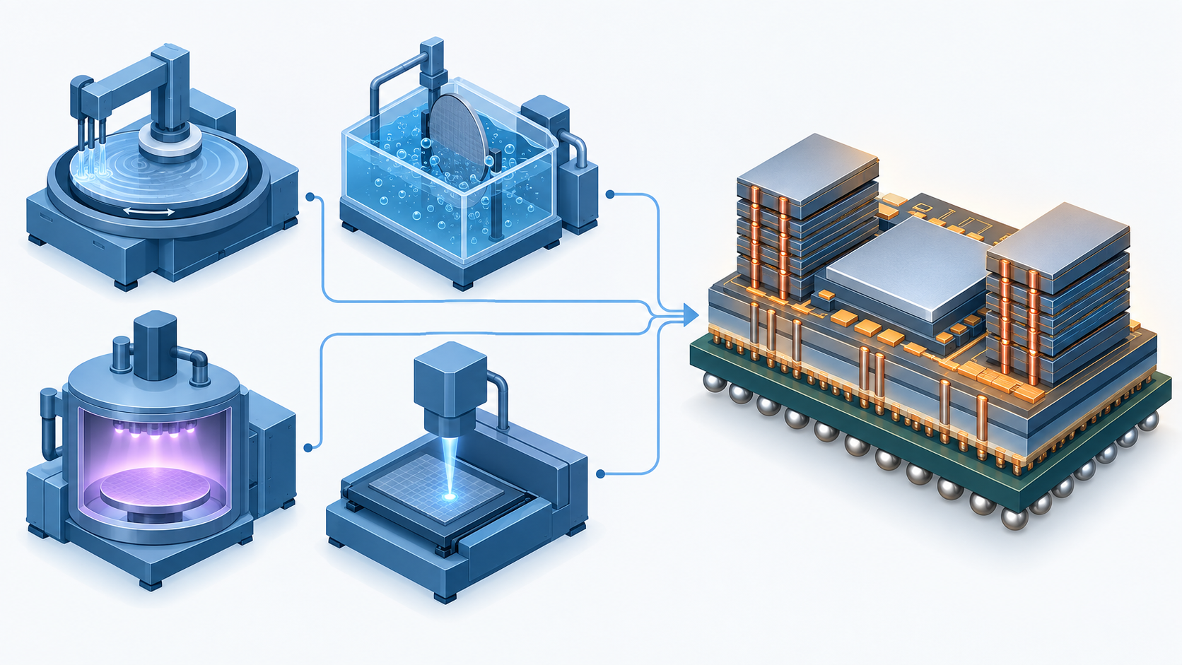
The back end used to be a comparatively rough mechanical business: dicing, wire bonding, encapsulation in resin. Once TSVs and hybrid bonding arrived, what the process demanded became flatness, film thickness and plating uniformity measured in single micrometres and below. That is precisely the capability front-end equipment has been sharpening for decades, and it is why Applied Materials can move into the back end at all. The products it announced for back-end use in 2026 are applications of four well-worn front-end technologies: CMP (polishing), ECD (electroplating), PECVD (plasma deposition) and eBeam metrology and defect review. Seen from the materials side, this means that polishing slurries, plating chemistries and precursor gases developed for the front end are now exposed to back-end specifications as they stand. And because the substrate changes from silicon to organic or glass, the demands on adhesion and thermal expansion are harsher than in the front end, not gentler.
4. Scale: five years of revenue
| Fiscal year (year end) | Revenue (US$m) | Operating income (US$m) | R&D expense (US$m) | Capex (US$m) |
|---|---|---|---|---|
| FY2021 (31 October 2021) | 23,063 | 6,889 | 2,485 | 668 |
| FY2022 (30 October 2022) | 25,785 | 7,788 | 2,771 | 787 |
| FY2023 (29 October 2023) | 26,517 | 7,654 | 3,102 | 1,106 |
| FY2024 (27 October 2024) | 27,176 | 7,867 | 3,233 | 1,190 |
| FY2025 (26 October 2025) | 28,368 | 8,289 | 3,570 | 2,260 |
Revenue, operating income, R&D expense and capital expenditure are all taken from the SEC's XBRL data, as tagged in each year's Form 10-K. FY2025 capex of US$2.26bn is 1.9 times the US$1.19bn of the previous year, and 3.4 times the level of five years earlier Our calculation.
Two things are worth reading closely here. The first is how gently the top line grows. The compound annual growth rate from FY2021 to FY2025 is 5.3% Our calculation, a different animal from the semiconductor companies that nearly tripled over the same period. An equipment maker sells to the rhythm of its customers building factories, so it feels chip demand a year or two after the chip makers do.
The second is the jump in capital spending, up 1.9 times year on year in FY2025 alone. When an equipment maker expands its own plants, it is working on the assumption that it is about to ship a great many tools. And so it proved: revenue accelerated sharply in FY2026, with third-quarter revenue (for the quarter ended 26 July 2026) of US$9.115bn, up 25% year on year and a quarterly record Sourced.
Where the 36,500 employees are
| Region | Share | Notes |
|---|---|---|
| Asia-Pacific | About 46% | Singapore, Taiwan, China, Korea, Japan, India and others |
| North America | About 42% | Headquarters in Santa Clara and the principal R&D sites |
| Europe and the Middle East | About 12% | Includes the manufacturing and development sites in Israel |
Regular employees as of 26 October 2025, across 25 countries. The Form 10-K carries no breakdown by education or job family of the kind TSMC publishes Not yet confirmed.
5. Company category and position in the back-end industry
The category is a manufacturer, specifically of semiconductor production equipment. Within the industry it sits one step upstream of the companies that make chips, such as TSMC, Samsung and Micron. It is upstream of the contract assemblers, the OSATs, as well, and an OSAT can perfectly well be an Applied Materials customer.
Applied Materials' back-end revenue appears neither in its statutory filings nor in its earnings releases Not yet confirmed. Figures of the form "X per cent of the advanced packaging market" or "US$Y bn of back-end tool revenue" come from research firms or the press, not from primary material, and this article does not use them. What the company itself says goes no further than a qualitative claim: that it holds leading positions in leading-edge logic, DRAM and advanced packaging Sourced.
What is disclosed is the split of Semiconductor Systems revenue by end market Sourced. HBM, high bandwidth memory, is classified under DRAM, so part of the back-end demand surfaces there.
| Semiconductor Systems revenue by market | FY2023 | FY2024 | FY2025 |
|---|---|---|---|
| Foundry, logic and other | 77% | 68% | 67% |
| DRAM (including HBM-related investment) | 17% | 28% | 26% |
| NAND flash memory | 6% | 4% | 7% |
The DRAM share has gone from 17% to 26% in two years. The company does not say how much of that increase is HBM-related Not yet confirmed.
6. Sites and the countries where it manufactures
Being an equipment maker, it has no fabs. What it has instead are assembly, integration and test plants, and development sites, scattered across the world Sourced.
| Function | Main countries | As the Form 10-K puts it |
|---|---|---|
| Headquarters | United States | Santa Clara, California |
| Manufacturing (principal) | United States, Singapore, Taiwan, Israel | Products are manufactured primarily in the United States, Singapore, Taiwan and Israel |
| Manufacturing and sourcing (overall) | United States, Singapore, Japan, China, Korea, Taiwan, Israel and others | A distributed manufacturing model, with manufacturing and supply chain activity in several countries |
| Product development and engineering | United States, India, Israel | Development is centred on these three countries |
| Customer demonstration | United States, China, Taiwan, Israel, Korea | Where customers run their own wafers on the tools before buying |
| Real estate | United States, Singapore, Taiwan, Israel, China, India | About 9.1 million square feet owned and about 5.3 million leased, plus about 279 acres of developable land |
Split revenue by where the tool was delivered and the map sharpens considerably Sourced.
The regional split of revenue is a map of where the customers' plants are. China at 30%, Taiwan at 24% and Korea at 20% come to 74% between them Our calculation. For anyone selling back-end materials, meaning plating chemistries, CMP slurries, underfill and mould compound, the place the tool goes and the place the material is needed are the same place. An equipment maker's regional revenue is therefore a usable leading indicator of where materials demand will appear. With one caveat: part of the China business falls within the reach of U.S. export controls, so reading that 30% as something that simply continues would be unwise (see section 11).
7. Leading products and share in semiconductor back-end work
The tools announced for back-end use in 2026
This is the part of the story that can be told concretely. The company names new products explicitly in its quarterly earnings releases, the press releases attached to its 8-K filings, and the third-quarter FY2026 release states plainly that it introduced six systems for DRAM and advanced packaging Sourced.
| Product | Technology | Role in the back end, as the company describes it |
|---|---|---|
| Opta Quad CMP | Chemical mechanical polishing | Designed specifically for advanced packaging. It watches the wafer continuously during polishing and adjusts in real time, improving within-wafer uniformity and total thickness variation. The company calls this particularly important for hybrid bonding |
| Nokota VMax 2 ECD | Electrochemical copper plating | One platform covering everything from filling TSVs for 3D stacking to fine-pitch wiring such as microbumps. It shapes the electric field dynamically to compensate for layout-driven variation |
| Producer Avila 2 PECVD | Plasma deposition | Improves the mechanical stability of ultra-thin DRAM dies. It deposits a stress-balanced dielectric around the TSVs so that 12-high, 16-high and taller HBM stacks become buildable |
| VeritySEM 7AP | eBeam dimensional metrology | Measures dimensions on thick, mixed-material, heavily warped substrates. It is built for the warpage that comes with HBM and chiplet structures, and is claimed to resolve below 10nm |
| SEMVision G7AP | eBeam defect review | Extends eBeam defect review into advanced packaging, with high-resolution review and automatic classification on silicon, organic and glass substrates |
| Centris Spectral SiN ALD and others | Atomic layer deposition and etch | These are front-end tools, for logic and 3D NAND. They appear in the same announcement as the back-end products, which makes the two easy to confuse |
All of the above are the company's own descriptions, as given in the third-quarter earnings release of 13 August 2026 (the press release attached to the 8-K). None of the performance claims has been independently verified.
In May 2026 the company also announced that it had signed an agreement to acquire the NEXX business of ASMPT Sourced. NEXX makes deposition equipment for large-area advanced packaging, and Applied describes the acquisition as a way to broaden its portfolio of panel-level advanced packaging technology. However, neither the price nor the expected closing date appears in the primary sources this article checked Not yet confirmed.
On market share, plainly
No primary source could be found for Applied Materials' share of the back-end equipment market Not yet confirmed. The company discloses neither share by tool type nor revenue from advanced packaging. Only three things can be stated from primary material.
- Advanced packaging is named explicitly in the Form 10-K's list of forces reshaping the industry — the company lists "the importance of advanced packaging for AI computing" among the factors that could materially hurt results if it responds badly Sourced
- It has named advanced packaging as a growth area in every quarter of 2026 — in the first quarter, "leading-edge logic, HBM and advanced packaging" were cited as the fastest-growing areas; in the third quarter, the company said it expected "strong growth in DRAM, leading-edge logic and advanced packaging" through the second half Sourced
- It is launching dedicated tools aimed squarely at the back end — as the table above shows Sourced
8. Current investment plans
An equipment maker's "investment" never looks like a foundry's enormous fab spending. What counts instead is R&D expense and the capacity to build tools.
R&D expense went from US$2.485bn in FY2021 to US$3.570bn in FY2025, up about 1.4 times in five years Our calculation. At 12.6% of revenue, that is above the average for chip makers.
On manufacturing capacity, the CFO said in the first-quarter FY2026 earnings release that the company had roughly doubled its equipment manufacturing capacity over the past several years, strengthened its supply chain and built inventory Sourced. In the third quarter it added that it would invest further in manufacturing capacity to support the demand outlook through the end of the decade, but neither the amount nor the timing has been published Not yet confirmed.
The EPIC Center is a collaborative research site in Silicon Valley, set up with the stated aim of dramatically shortening the time it takes to commercialise a technology from early research to volume production. Samsung Electronics was the first chip maker to announce its participation, in February 2026; TSMC, SK hynix, Micron, Advantest and three universities followed in May, and Broadcom, SCREEN SPE and the University of California, Berkeley in August, bringing the total to 11 collaborations by the third quarter Sourced. From a back-end point of view, the important additions are Broadcom and Advantest. Broadcom joined to accelerate "advanced packaging technologies essential to next-generation AI systems"; Advantest to tie front-end manufacturing technology more closely to back-end test of chips and packages. The amount invested in the EPIC Center, the size of the building and its exact location have not been published Not yet confirmed.
9. Major corporate partners
Applied Materials' partnerships are not equity ties or joint ventures of the sort TSMC forms. They are joint development and joint research, almost without exception. Listed below are only those the company has named itself, in its own earnings releases Sourced.
| Counterparty | Kind | Substance | Announced |
|---|---|---|---|
| Samsung Electronics | EPIC Center partner | The first chip maker to announce that it would join the EPIC Center | February 2026 |
| TSMC | EPIC Center innovation partner | Joint development across materials engineering, equipment and process integration, aimed at power efficiency from the data centre to the edge | May 2026 |
| SK hynix | Long-term collaboration agreement | Next-generation DRAM and HBM. Engineers from both companies work side by side at the EPIC Center on materials, process integration and 3D advanced packaging | May 2026 |
| Micron Technology | Joint development | Next-generation DRAM, HBM and NAND, linking the EPIC Center in Silicon Valley with Micron's Boise site | May 2026 |
| Advantest | EPIC Center innovation partner | Connecting front-end manufacturing technology with back-end test of chips and packages | May 2026 |
| Broadcom | EPIC Center innovation partner | Accelerating advanced packaging technologies essential to next-generation AI systems | August 2026 |
| SCREEN Semiconductor Solutions | EPIC Center innovation partner | Co-optimisation of wafer cleaning technology with materials engineering | August 2026 |
| ASMPT | Business acquisition (agreement signed) | An agreement to acquire the NEXX business, which makes deposition equipment for large-area advanced packaging. Price and closing date not disclosed | May 2026 |
| Stanford University and others | Research partners | Arizona State University, Rensselaer Polytechnic Institute, Stanford University and the University of California, Berkeley have joined the EPIC Center | May and August 2026 |
| Synopsys and NVIDIA | Joint research | Accelerating materials modelling for AI and quantum chemistry research. Not directly related to the back end | May 2026 |
| EssilorLuxottica | Long-term joint development agreement | Optics for smart glasses. A separate field from semiconductor packaging | August 2026 |
Applied Materials does not disclose customer names. All the Form 10-K gives is a ratio: in FY2025, two customers accounted for about 19% and about 15% of revenue. The names are withheld Not yet confirmed. TSMC, Samsung, SK hynix and Micron appear in the table above because the company named them itself as joint research counterparties, not as customers, and nothing is known about transaction values or which tools were bought.
10. Where the company is heading in this field
Facts and outlook are kept apart here as well.
What is established
| Fact | What it implies for the back end |
|---|---|
| Third-quarter FY2026 revenue of US$9.115bn, up 25% year on year and a quarterly record | The demand cycle has clearly turned. Back-end products are part of that total |
| Fourth-quarter guidance of US$10.25bn plus or minus US$500m | The company itself is planning on acceleration |
| Six tools launched for back-end use in 2026 (CMP, plating, deposition, metrology, defect review) | The redirection of front-end technology into the back end has taken product form |
| Agreement to acquire ASMPT's NEXX business (panel-level advanced packaging deposition) | Panel formats, larger than a wafer, were covered by acquisition rather than in-house development |
| Broadcom (advanced packaging) and Advantest (back-end test) joined the EPIC Center | The company is providing the venue where front end and back end meet |
| FY2025 capital expenditure up 1.9 times year on year | Supply capacity for tools is being built ahead of the orders |
Outlook
Not yet confirmed Read plainly, the facts above point towards Applied Materials' presence in the back end strengthening for now. The reason is that the back end is turning from machining into thin-film processing, and no one carries a broader range of thin-film tools than this company. Hybrid bonding is, in the end, a contest of flatness and cleanliness; a TSV is copper plating into a deep hole; taller HBM stacks are a problem of stress-controlled thin films. Every one of those is an extension of what Applied has been doing in the front end for more than thirty years.
Not yet confirmed The ways this reading could fail are equally clear. First, the bonder itself is not an Applied Materials product. Bonding tools belong to specialists such as ASMPT and Besi; what Applied has brought out are the tools either side of that step. Second, tool prices in the back end are not as high as in the front end, so unit economics differ. Third, most of the demand is concentrated on AI, and if AI investment slows, a plateau like the one in 2023 will return. The company says as much in its own Form 10-K: AI is changing rapidly, the timing and scale of AI-related investment can vary greatly, and AI-related demand is therefore difficult to forecast accurately Sourced.
11. The risks this company carries
What follows is drawn from the risk factors the company sets out in its Form 10-K, narrowed to those that matter in a back-end context Sourced.
| Risk | Substance | Supporting figures or wording |
|---|---|---|
| Export controls on China | The company itself writes that U.S. export controls on China may help domestic Chinese equipment makers grow and may favour foreign competitors that are not subject to those controls | FY2025 revenue from China was US$8.529bn, 30% of the total Our calculation |
| Government investigations | Since 2022 the company has received several subpoenas from the U.S. Department of Justice, the Commerce Department's Bureau of Industry and Security and the SEC, concerning shipments to Chinese customers and export control compliance. It has received further subpoenas and states that it may receive more | Stated in the Form 10-K. Neither the outcome nor any financial effect is settled Not yet confirmed |
| Customer concentration | Two customers were about 34% of FY2025 revenue between them. The ratio moves a great deal from year to year | 19% and 15% in FY2025; 12% and 11% in FY2024; 19% and 15% in FY2023 |
| Industry cyclicality | Revenue follows the cycle on which customers build factories. The company states plainly that changes in demand have a significant effect on results | Revenue growth slowed to +3% in FY2023 and +2% in FY2024 Our calculation |
| Difficulty of forecasting AI demand | AI is the largest demand driver, yet the company states that the timing and scale of that investment can vary greatly | Set out at the head of the risk factors in the Form 10-K |
| Inventory and capacity built ahead | Inventory and manufacturing capacity have been built in anticipation of demand. If demand falls short, write-downs follow | FY2025 capital expenditure was 1.9 times the previous year Our calculation |
Export controls on equipment move the geography of materials demand along with the tools. A structure in which China is 30% of revenue means that if tools stop entering Chinese plants, the slurry and plating chemistry those tools would have consumed are no longer needed either. And if domestic Chinese equipment makers grow in their place, a separate lineage of materials specifications grows up to match them. For a materials supplier that means maintaining two specification families for the same application: unglamorous, and genuinely expensive. Back-end materials tend to be less exposed to controls than front-end ones, but if the tool stops, the result is identical.
12. Glossary
- Front end and back end
- The front end runs up to the point where circuits are built on the wafer. The back end covers dicing, stacking, encapsulation and test. This article is about the back end.
- CMP
- Chemical mechanical polishing. A slurry and a pad flatten the surface to within nanometres. It is the precondition for hybrid bonding.
- ECD
- Electrochemical deposition, or electroplating. Copper is deposited electrically from a plating bath, used to fill TSVs and to form microbumps.
- PECVD
- Plasma enhanced chemical vapour deposition. A plasma assists the reaction so films can be grown at low temperature, which matters in a back end that cannot take heat.
- TSV
- Through-silicon via. A vertical interconnect that passes through the chip and joins dies stacked above and below.
- Hybrid bonding
- Joining two surfaces of copper and dielectric directly, with no solder bumps. Flatness and cleanliness of the bonding surface decide everything.
- Panel-level packaging
- Building packages on a large rectangular substrate, a panel, rather than a round wafer. More units come off each sheet, and large AI dies are easier to place.
- Form 10-K
- The annual report a U.S.-listed company files with the Securities and Exchange Commission. It is audited and carries legal liability for its contents.
 AI-generated concept
13. References
- Applied Materials Form 10-K for the fiscal year ended October 26, 2025 (filed with the U.S. SEC on 12 December 2025). Revenue, operating income and segment results, headcount and its regional split, revenue by region, customer concentration, revenue by end market, sites and countries of manufacture, the description of the advanced packaging tools, and risk factors. https://www.sec.gov/Archives/edgar/data/6951/000162828025056742/amat-20251026.htm
- Applied Materials Fourth quarter and full year FY2025 earnings release (Form 8-K, Exhibit 99.1, 13 November 2025). Full-year FY2025 revenue of US$28.368bn, up 4% year on year, segment revenue and operating income, and display revenue. https://www.sec.gov/Archives/edgar/data/6951/000162828025051998/exhibit991q42025earningsre.htm
- Applied Materials Third quarter FY2026 earnings release (Form 8-K, Exhibit 99.1, 13 August 2026). Quarterly revenue of US$9.115bn, up 25% year on year, fourth-quarter guidance, the six new back-end systems, the 11 EPIC Center collaborations, the addition of Broadcom, SCREEN SPE and UC Berkeley, and the US$500m Tampines campus in Singapore. https://www.sec.gov/Archives/edgar/data/6951/000162828026056699/exhibit991q32026earningsre.htm
- Applied Materials Second quarter FY2026 earnings release (Form 8-K, Exhibit 99.1, 14 May 2026). The EPIC Center additions of TSMC, SK hynix, Micron, Advantest and three universities, the agreement to acquire ASMPT's NEXX business, the work with Synopsys and NVIDIA, and a 15% dividend increase. https://www.sec.gov/Archives/edgar/data/6951/000162828026035071/exhibit991q22026earningsre.htm
- Applied Materials First quarter FY2026 earnings release (Form 8-K, Exhibit 99.1, 12 February 2026). Samsung Electronics joining the EPIC Center, the CFO's statement that manufacturing capacity has roughly doubled over the past several years, and the move of the 200mm business between segments. https://www.sec.gov/Archives/edgar/data/6951/000162828026007661/exhibit991q12026earningsre.htm
- U.S. SEC EDGAR XBRL company facts API (CIK 0000006951). Revenue, operating income, R&D expense and capital expenditure for FY2021 to FY2025, as tagged in each year's Form 10-K. https://data.sec.gov/api/xbrl/companyfacts/CIK0000006951.json
14. Claim-to-source audit
| Claim in the article | Category | Source |
|---|---|---|
| Legal name, head office address, year founded (1967), Delaware incorporation, NASDAQ listing (AMAT) | Sourced | Reference 1 https://www.sec.gov/Archives/edgar/data/6951/000162828025056742/amat-20251026.htm |
| The fiscal year ends on the last Sunday in October; FY2025 ran 28 October 2024 to 26 October 2025 | Sourced | Reference 1 https://www.sec.gov/Archives/edgar/data/6951/000162828025056742/amat-20251026.htm |
| FY2025 revenue of US$28.368bn, up 4% year on year | Sourced | Reference 2 https://www.sec.gov/Archives/edgar/data/6951/000162828025051998/exhibit991q42025earningsre.htm |
| Revenue, operating income, R&D expense and capex for FY2021 to FY2025 | Sourced | Reference 6 https://data.sec.gov/api/xbrl/companyfacts/CIK0000006951.json |
| The 5.3% compound growth rate, the year-on-year percentages, capex at 1.9 times, R&D at 12.6% of revenue, and the regional shares | Our calculation | Derived from the figures in references 6 and 1 https://data.sec.gov/api/xbrl/companyfacts/CIK0000006951.json |
| Segment revenue (Semiconductor Systems 73%, AGS 23%, other 4%) and operating margins | Sourced | Reference 2 https://www.sec.gov/Archives/edgar/data/6951/000162828025051998/exhibit991q42025earningsre.htm |
| About 36,500 employees, 25 countries, regional split of 46% / 42% / 12% | Sourced | Reference 1 https://www.sec.gov/Archives/edgar/data/6951/000162828025056742/amat-20251026.htm |
| Revenue by region (China 8,529 / Taiwan 6,857 / Korea 5,608 / United States 3,063 and the rest) | Sourced | Reference 1 https://www.sec.gov/Archives/edgar/data/6951/000162828025056742/amat-20251026.htm |
| Customer concentration (two customers at 19% and 15% in FY2025) | Sourced | Reference 1 https://www.sec.gov/Archives/edgar/data/6951/000162828025056742/amat-20251026.htm |
| Countries of manufacture, development and demonstration; owned and leased floor area; the 279 acres of land | Sourced | Reference 1 https://www.sec.gov/Archives/edgar/data/6951/000162828025056742/amat-20251026.htm |
| How the advanced packaging tools are positioned (heterogeneous integration) | Sourced | Reference 1 https://www.sec.gov/Archives/edgar/data/6951/000162828025056742/amat-20251026.htm |
| The six new back-end systems (Opta Quad CMP, Nokota VMax 2 ECD, Producer Avila 2 PECVD, VeritySEM 7AP, SEMVision G7AP and others) | Sourced | Reference 3 https://www.sec.gov/Archives/edgar/data/6951/000162828026056699/exhibit991q32026earningsre.htm |
| Third-quarter FY2026 revenue of US$9.115bn, up 25%, and fourth-quarter guidance of US$10.25bn | Sourced | Reference 3 https://www.sec.gov/Archives/edgar/data/6951/000162828026056699/exhibit991q32026earningsre.htm |
| The 11 EPIC Center collaborations, the addition of Broadcom, SCREEN SPE and UC Berkeley, and the US$500m Tampines campus | Sourced | Reference 3 https://www.sec.gov/Archives/edgar/data/6951/000162828026056699/exhibit991q32026earningsre.htm |
| The EPIC Center additions of TSMC, SK hynix, Micron, Advantest and three universities, and the ASMPT NEXX acquisition agreement | Sourced | Reference 4 https://www.sec.gov/Archives/edgar/data/6951/000162828026035071/exhibit991q22026earningsre.htm |
| Samsung Electronics joining the EPIC Center, the CFO's comment on doubling capacity, and the 200mm segment move | Sourced | Reference 5 https://www.sec.gov/Archives/edgar/data/6951/000162828026007661/exhibit991q12026earningsre.htm |
| Export controls on China, the government subpoenas, the difficulty of forecasting AI demand and the other risk factors | Sourced | Reference 1 https://www.sec.gov/Archives/edgar/data/6951/000162828025056742/amat-20251026.htm |
| Revenue from back-end work (advanced packaging) | Not yet confirmed | Not disclosed. It sits inside Semiconductor Systems with no breakdown, so this article states no figure |
| Share of the back-end equipment market | Not yet confirmed | No primary source exists, so this article states no figure |
| The price and closing date of the ASMPT NEXX acquisition | Not yet confirmed | Absent from the primary sources this article checked |
| The investment in the EPIC Center, its size and its exact location | Not yet confirmed | Only "Silicon Valley" is published, and this article goes no further |
| The names of the two customers at 19% and 15% of revenue | Not yet confirmed | The company does not name its customers, and this article does not guess |
| How much of DRAM revenue is HBM-related | Not yet confirmed | The split is not published, so this article states no figure |
| The amount and timing of further capacity investment through the end of the decade | Not yet confirmed | Only the intention is published; this article could not confirm a figure |
| The outlook in section 10 | Not yet confirmed | An interpretation by this article, drawn from the six items in the facts table |
Last updated 21 September 2026 / Troy Technical
Every figure in this article comes from Applied Materials' statutory filings with the U.S. Securities and Exchange Commission or from the company's own announcements. No research-firm estimates or press-based figures have been used.